The document summarizes a student project involving the fabrication and characterization of CMOS devices and circuits using VLSI design processes. The students designed digital inverters and oscillators using CMOS technology in simulation software then fabricated the devices in a clean room using photolithography, etching, diffusion, and other microfabrication techniques to create n-type and p-type MOSFETs on a silicon chip. They then characterized the fabricated devices by measuring I-V curves and the oscillator's voltage, period, and frequency. The measured results were compared to pre-fabrication simulations to evaluate performance and identify non-ideal characteristics.
Reduced channel length cause departures from long channel behaviour as two-dimensional potential distribution and high electric fields give birth to Short channel effects.
Report contains digital and analog design flow procedures in detail, working, Simulation and Synthesize mapped output. Full custom Schematic and layout design by using virtuoso encounter cadence tool.
Routing in Integrated circuits is an important task which requires extreme care while placing the modules and circuits and connecting them with each other.
Physical verification will verify that the post-layout netlist and the layout are equivalent. i.e. all connections specified in the netlist is present in the layout. This article explains physical verification.
I made this presentation for you , I hope its useful for you all, and I hate Plagiarism please, I also used some slides here but I mentioned all in the last slide :)
Hope you can get benefits from it
An application-specific IC (ASIC) can be either a digital or an analog circuit. As their name implies, ASICs are not reconfigurable; they perform only one specific function. For example, a speed controller IC for a remote control car is hard-wired to do one job and could never become a microprocessor. An ASIC does not contain any ability to follow alternate instructions.
Effective Approach to Extract CMOS Model Parameters Based On Published Wafer ...IJERA Editor
The VLSI electronic circuit designs have steadily grown in their capacity and complexity through the years. MOSIS fabrication services provide test data that designers can used to simulate their circuit designs. The provided test results are extracted from various lot wafers and BSIM3 or BSIM4 model card parameters in addition to technology parameters are provided. It may be cumbersome to ensure design functionality over the wide range of model set of parameters. In this paper, it is proposed to utilize the average model parameters to validate circuit design functionality. It can be shown through device characterization and simple circuit simulations that the average model parameters can provide a good representation of the wide range of supplied model parameters. This is specially attractive for students of circuit design classes where classroom and graduate research work were computing resources are limited. Utilizing average model parameters alleviate the need to run simulations over the large set of models from the fabrication facility.
3d printer electronics engineering live projects abstracts @1000KV Technologi...1000kv technologies
electronics engineering live projects abstracts
electronics projects, electronics projects for engineering final year students, electronics and communication engineering projects for final year students,100kv,1000kv,1000kv technologies,1000kv projects,technologies,live projects,Hyderabad live projects,live projects in, diploma low cost projects,1000kv projects, , academic projects,btech live projects,Hyderabad,1000kilovolts,1000kilovolts technologies ,btech main projects ,
Presentation of a fault tolerance algorithm for design of quantum-dot cellul...IJECEIAES
A novel algorithm for working out the Kink energy of quantum-dot cellular automata (QCA) circuits and their fault tolerability is introduced. In this algorithm at first with determining the input values on a specified design, the calculation between cells makes use of Kink physical relations will be managed. Therefore, the polarization of any cell and consequently output cell will be set. Then by determining missed cell(s) on the discussed circuit, the polarization of output cell will be obtained and by comparing it with safe state or software simulation, its fault tolerability will be proved. The proposed algorithm was implemented on a novel and advance fault tolerance full adder whose performance has been demonstrated. This algorithm could be implemented on any QCA circuit. Noticeably higher speed of the algorithm than simulation and traditional manual methods, expandability of this algorithm for variable circuits, beyond of four-dot square of QCA circuits, and the investigation of several damaged cells instead just one and special cell are the advantages of algorithmic action.
Call for paper - International Joural of Microelectronics Engineering(IJME)IJMEJournal1
International Journal of Microelectronics Engineering invites high quality manuscripts in the research areas of analog and digital circuit design methodologies. This journal provides a worldwide, regular and comprehensive update on microelectronics engineering. Journal invites significant research and application papers in all the areas listed below. The comprehensive review papers covering recent developments will also be considered.
CALL FOR PAPER -INTERNATIONAL JOURNAL OF MICROELECTRONICS ENGINEERINGIJMEJournal1
International Journal of Microelectronics Engineering invites high quality manuscripts in the research areas of analog and digital circuit design methodologies. This journal provides a worldwide, regular and comprehensive update on microelectronics engineering. Journal invites significant research and application papers in all the areas listed below. The comprehensive review papers covering recent developments will also be considered.
Design and test challenges in Nano-scale analog and mixed CMOS technology VLSICS Design
The continuous increase of integration densities in Complementary Metal–Oxide–Semiconductor (CMOS) technology has driven the rapid growth of very large scale integrated (VLSI) circuit for today's high-tech electronics industries from consumer products to telecommunications and computers. As CMOS technologies are scaled down into the nanometer range, analog and mixed integrated circuit (IC) design and testing have become a real challenge to ensure the functionality and quality of the product. The first part of the paper presents the CMOS technology scaling impact on design and reliability for consumer and critical applications. We then propose a discussion on the role and challenges of testing analog and mixed devices in the nano-scale era. Finally we present the IDDQ testing technique used to detect the most likely defects of bridging type occurring in analog CMOS circuits during the manufacturing process and creating a resistive path between VDD supply and the ground. To prove the efficiency of the proposed technique we design a CMOS 90nm operational amplifier (Opamp) and a Built in Current Sensor (BICS) to validate the technique and correlate it with post layout simulation results.
ATIPS - Advanced Technology Information Processing SystemsWael Badawy
Advanced Technology Information Processing Systems
this presentation was provided in the Canada Taiwan meeting in April 2005.
Graham.A. Jullien, iCORE Research Chair,
Wael Badawy, iCORE Research Associate and Director of the Digital Video Laboratory,
Dr. V.S. Dimitrov, iCORE Research Associate and member of the Centre for Information Securityand Cryptography
Dr. O. Yadid-Pecht, iCORE Research Associate, Imaging and Sensor Technology Laboratory
Toward an Electrically-Pumped Silicon Laser Modeling and Optimization
VLSI STEM Poster
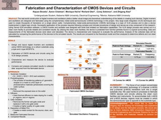
1. Fabrication and Characterization of CMOS Devices and Circuits
Kejuan Brooks1, Aaron Chatman1, Monique Harris1 Richard Oteri1 , Corey Solomon1, and Zhigang Xiao2
1Undergraduate Student, Alabama A&M University, Electrical Engineering; 2Mentor, Alabama A&M University
Abstract The real-world construction of digital inverters and oscillators yields a better visual image and theoretical understanding of the details in creating such devices. Digital inverters
and oscillators are designed and fabricated using the complementary metal-oxide-semiconductor (CMOS) technology in this project. Very large scale integration (VLSI) techniques are
used to create thousands of transistors on a single silicon wafer. Complementary metal-oxide-semiconductor (CMOS) technology is a type of VLSI process and is also a device
implemented in digital logic circuits. Successful application of the process requires following complex and intricate procedures of design and serves as a key component of the research.
Using Tanner EDA simulation software, a CMOS inverter and oscillator was designed with limits that imitated our fabrication capabilities. The VLSI design process was carried out in a
clean room facility to provide reliable and consistent results. By utilizing the clean room facilities, the device is protected from harmful particles found in a typical surrounding. Data and
measurements of the fabricated devices were taken and tabulated. The device is characterized and measured to evaluate the performance. Analysis of the collected data will be
calculated by comparing the performance of the devices to the simulated results. The results are compared to the theoretical model and then analyzed to determine defects and non-ideal
characteristics.
Acknowledgements We would like to thank Dr.
Zhigang Xiao for sharing his knowledge and experience
in IC design and the fabrication process. We would also
like to thank Alabama A&M University’s Department of
Electrical Engineering and Computer Science for the use
of the facilities and materials needed to conduct our
project.
GOALS
1. Design and layout digital inverters and oscillators
using CMOS technology on a silicon substrate using
p-type and n-type MOSFETs.
2. Fabrication of CMOS devices and circuits using the
VLSI design process.
3. Characterize and measure the device to evaluate
performance.
4. Compare and analysis simulated results to collected
data acquired from the fabricated device.
I-V Curves for nMOS
-0.0045
-0.004
-0.0035
-0.003
-0.0025
-0.002
-0.0015
-0.001
-0.0005
0
0.0005
-8 -6 -4 -2 0
Series1
Series2
Series3
Series4
Series5
Series6
Series7
Series8
0.00E+00
1.00E-04
2.00E-04
3.00E-04
4.00E-04
5.00E-04
6.00E-04
7.00E-04
8.00E-04
9.00E-04
1.00E-03
0 2 4 6 8
Series1
Series2
Series3
Series4
Series5
Series6
I-V Curves for pMOS
RESULTS
SUMMARY The focus of our project concentrates
on CMOS fabrication technology of n-channel (n-MOS)
and p-channel (p-MOS) transistors built into a single
substrate chip. We used hands-on processes to fabricate
CMOS devices and circuits utilizing the clean room
facilities and instruments. To accommodate both n-MOS
and p-MOS devices, regions must be created in which
the semiconductor type is opposite to the substrate type.
APPROACH
1. Substrate Oxidation
▪ Si + 2H2O = SiO2 + 2H2 (wet oxidation)
2. Photolithography
▪ The process of transferring patterns of geometric
shapes on a mask to a thin layer of
photosensitive materials (photoresist) covering the
wafer surface
3. Etching
▪ Removed the exposed area on the wafer
4. Diffusion
▪ Used thermal diffusion to make doping for n wells,
p+ regions, and n+ regions
5. Gate Oxidation
▪ Removes the former wet gate oxide and
replaces it with a dry gate oxide
▪ Creates a higher quality of a gate oxide
6. Deposition of Metal Film
▪ Creates a metal contact for the source, drain, and
gate
7. Measured Fabricated Devices
8. Compared Results
Simulated Results
Peak-to-Peak Voltage Period (T) Frequency
5V 0.7 µs 1.429 MHz
Fabricated Results
Peak-to-Peak Voltage Period (T) Frequency
3V 0.75 µs 1.333 MHz
Simulated Oscillation Frequency
Fabricated CMOS Oscillator