Download as PDF, PPTX


![ARM7 Datapath Overview
multiply
data out register
instruction
decode
&
control
incrementer
register
bank
address register
barrel
shifter
A[31:0]
D[31:0]
data in register
ALU
control
P
C
PC
A
L
U
b
u
s
A
b
u
s
B
b
u
s
register
FETCH
DECODE
EXECUTE
(WB)
*Pipeline registers are omitted](https://image.slidesharecdn.com/unitiiarm7introl-150323003420-conversion-gate01/75/Unit-II-Arm-7-Introduction-17-2048.jpg)
![18
ARM7TDMI Interface Signals (1/4)
mreq
seq
lock
Dout[31:0]
D[31:0]
r/w
mas[1:0]
mode[4:0]
trans
abort
opc
cpi
cpa
cpb
memory
interface
MMU
interface
coprocessor
interface
mclk
wait
eclk
isy nc
bigend
enin
irq
¼q
reset
enout
abe
Vdd
Vss
clock
control
configuration
interrupts
initialization
bus
control
power
ale
ape
dbe
dbgrq
breakpt
dbgack
debug
exec
extern1
extern0
dbgen
bl[3:0]
TRST
TCK
TMS
TDI
JTAG
controls
TDO
Tbit st atetbe
rangeout0
rangeout1
dbgrqi
commrx
commtx
enouti
highz
busdis
ecapclk
busen
Din[31:0]
A[31:0]
ARM7TDMI
core
tapsm[3:0]
ir[3:0]
tdoen
tck1
tck2
screg[3:0]
TAP
information
driv ebs
ecapclkbs
icapclkbs
highz
pclkbs
rstclkbs
sdinbs
sdoutbs
shclkbs
shclk2bs
boundary
scan
extension](https://image.slidesharecdn.com/unitiiarm7introl-150323003420-conversion-gate01/75/Unit-II-Arm-7-Introduction-18-2048.jpg)
![24TM 2439v10 The ARM Architecture
When the processor is executing in ARM state:
All instructions are 32 bits wide
All instructions must be word aligned
Therefore the pc value is stored in bits [31:2] with bits [1:0] undefined (as
instruction cannot be halfword or byte aligned).
When the processor is executing in Thumb state:
All instructions are 16 bits wide
All instructions must be halfword aligned
Therefore the pc value is stored in bits [31:1] with bit [0] undefined (as
instruction cannot be byte aligned).
When the processor is executing in Jazelle state:
All instructions are 8 bits wide
Processor performs a word access to read 4 instructions at once
Program Counter (r15)](https://image.slidesharecdn.com/unitiiarm7introl-150323003420-conversion-gate01/75/Unit-II-Arm-7-Introduction-24-2048.jpg)


This document provides an introduction to the ARM-7 microprocessor architecture. It describes key features of the ARM7TDMI including its 32-bit RISC instruction set, 3-stage pipeline, 37 registers including separate registers for different processor modes, and low power consumption. The document also compares RISC and CISC architectures and summarizes the different versions of the ARM architecture.
Overview of ARM-7 presented by Dr. P. H. Zope, with contact information.
ARM stands for Advanced RISC Machine, highlighting its leadership in low-power, cost-sensitive embedded applications.
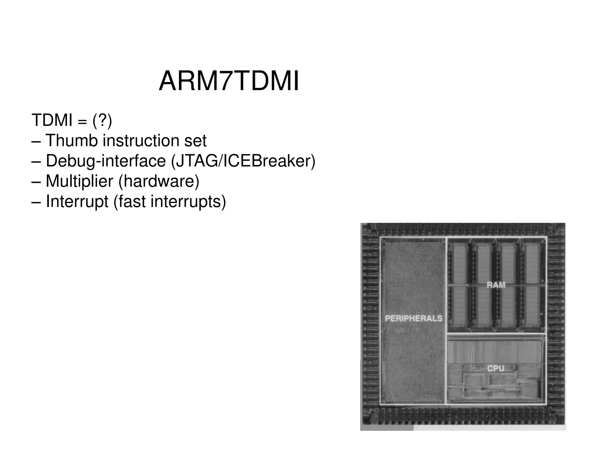
ARM7TDMI includes Thumb instruction set, JTAG interface for debugging, hardware multiplier, and fast interrupts.
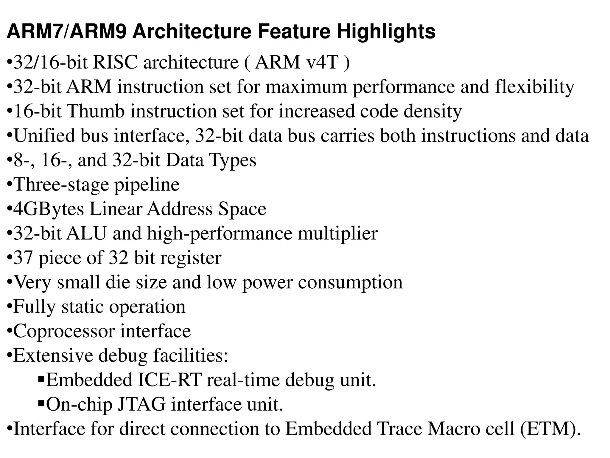
Details on ARM v4T architecture featuring 32/16-bit support, pipeline, and low power consumption among others.
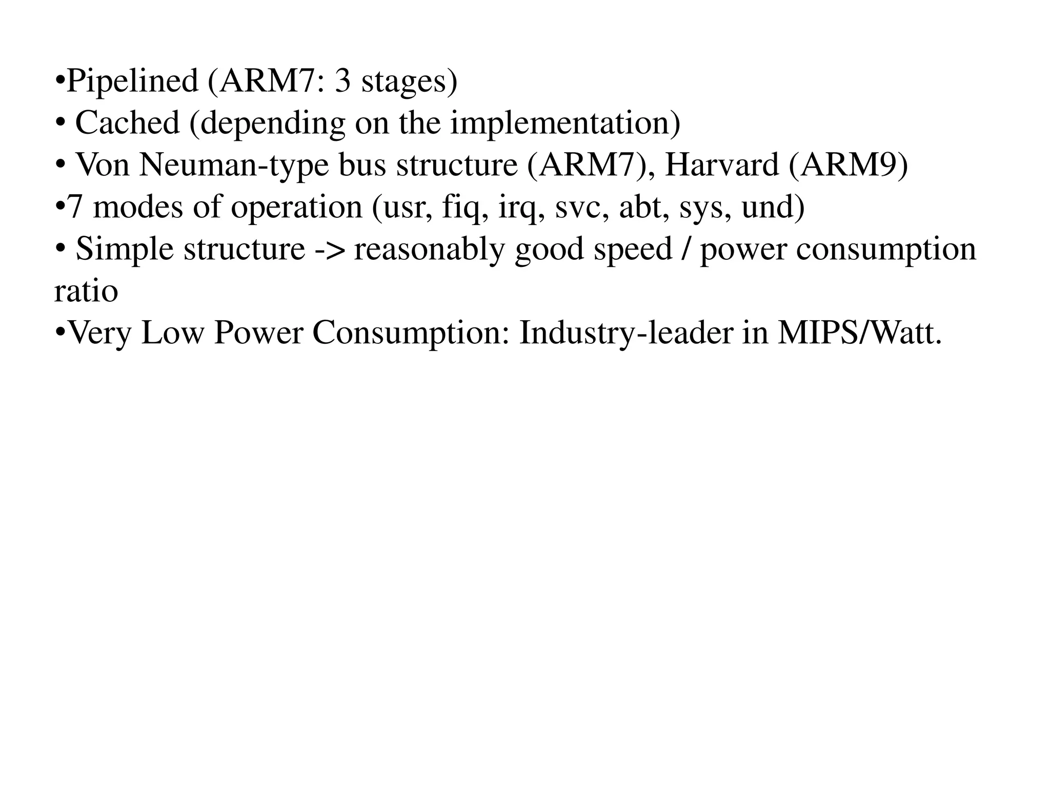
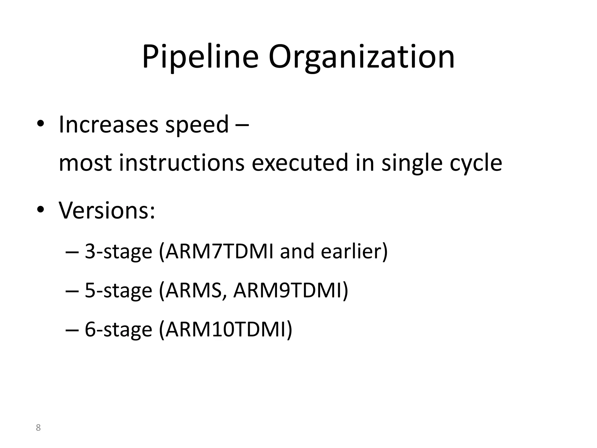
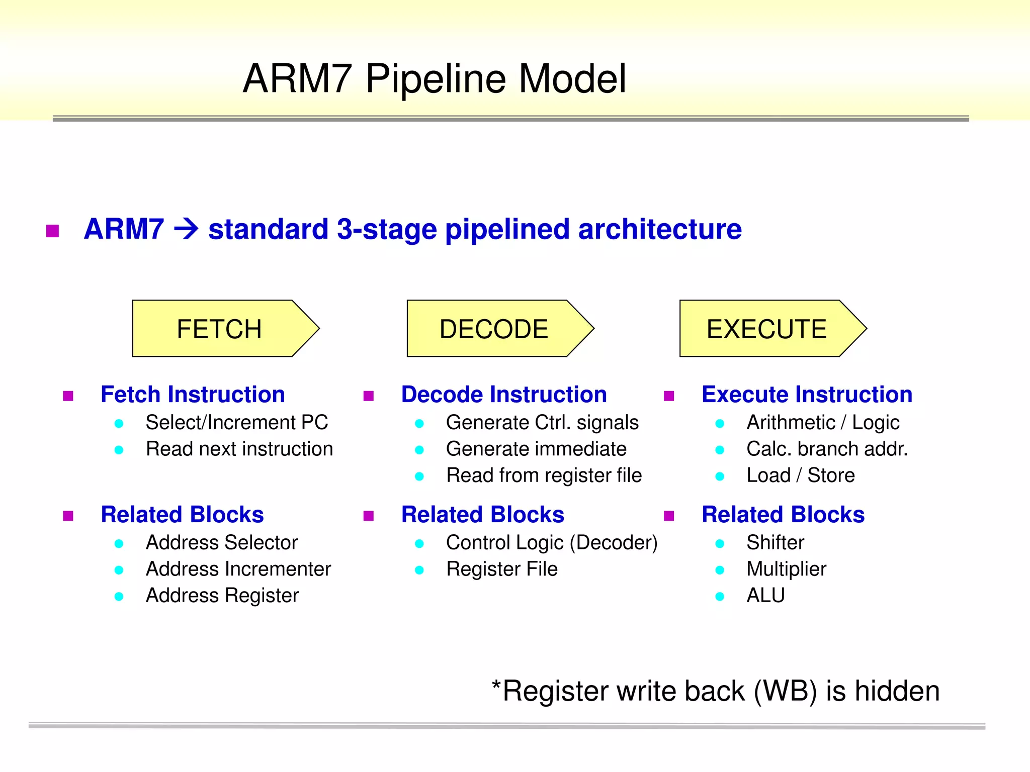
ARM7 features a 3-stage pipelined architecture emphasizing speed with low power consumption.
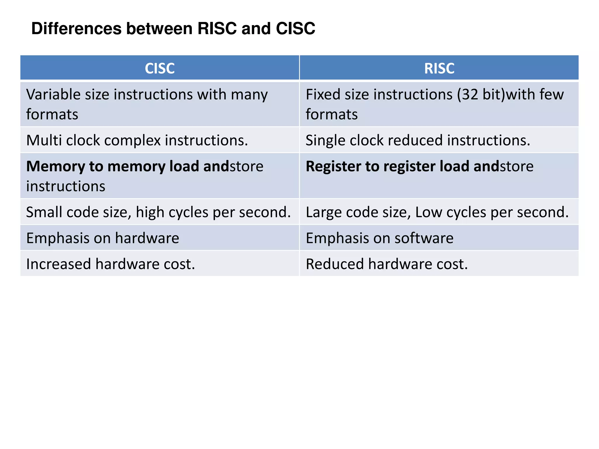
Contrast of RISC (Reduced Instruction Set Computing) and CISC (Complex Instruction Set Computing) architectures.
Presentation of various products powered by ARM technology.
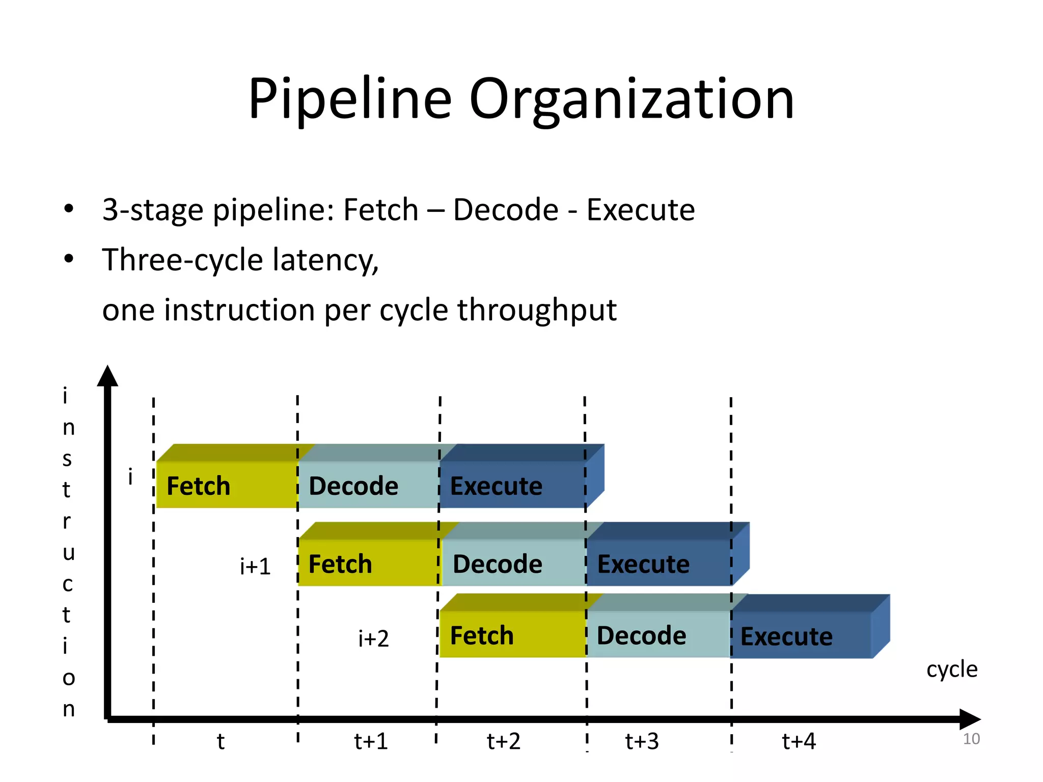
Details of pipeline organization, including various stages in ARM architectures.
Diagrammatic representation of ARM7's pipeline stages: Fetch, Decode, Execute with detailed descriptions.
Visually explaining instruction execution in a 3-stage pipeline with cycles.
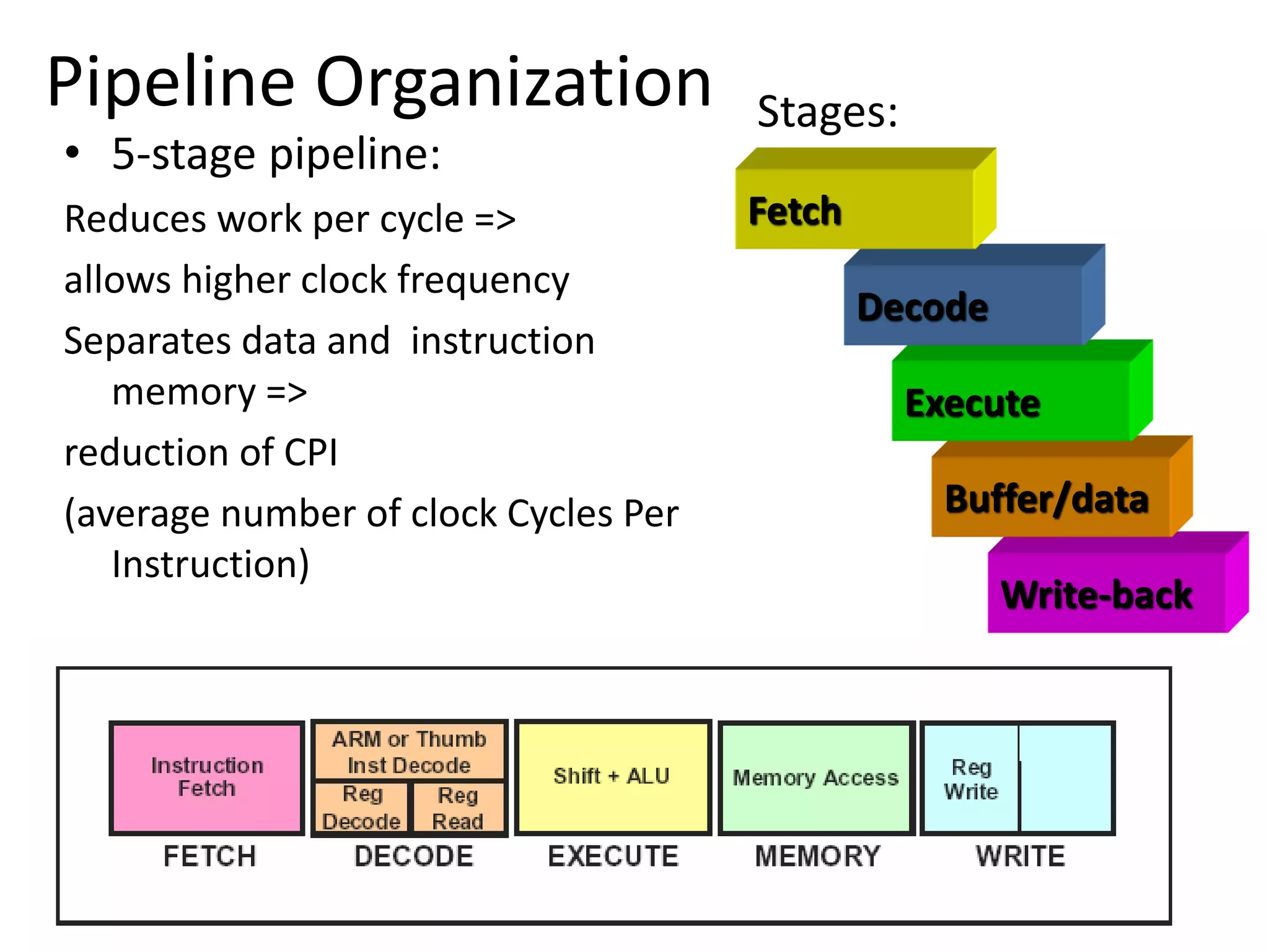
Outlining benefits of 5-stage pipeline architecture, which allows for higher clock frequency.
Explanation of how pipelines are flushed and refilled during branches to avoid slowdowns.
General overview of ARM-7 architecture.
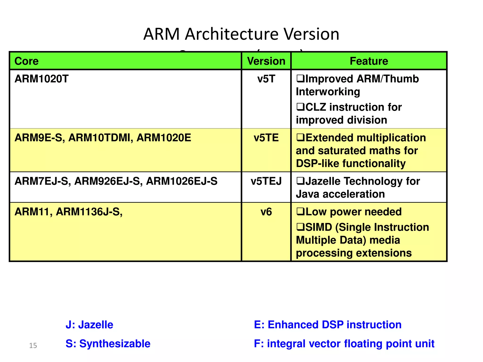
Summary of features across different ARM architecture versions and enhancements.
Continuing summary of ARM architecture features including multimedia and DSP functionality.
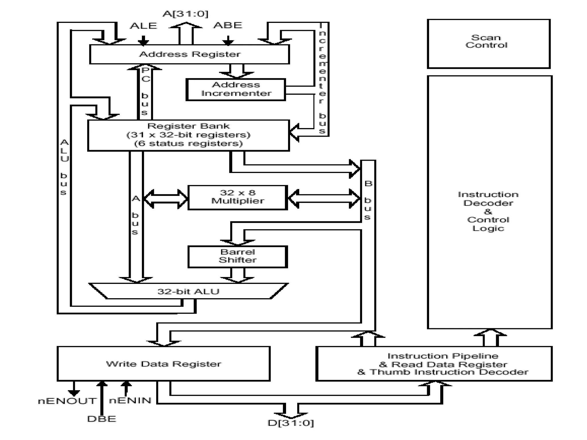
Overview of ARM7 data path components including ALU, registers, and pipeline stages.
Examination of the various interface signals within ARM7TDMI.
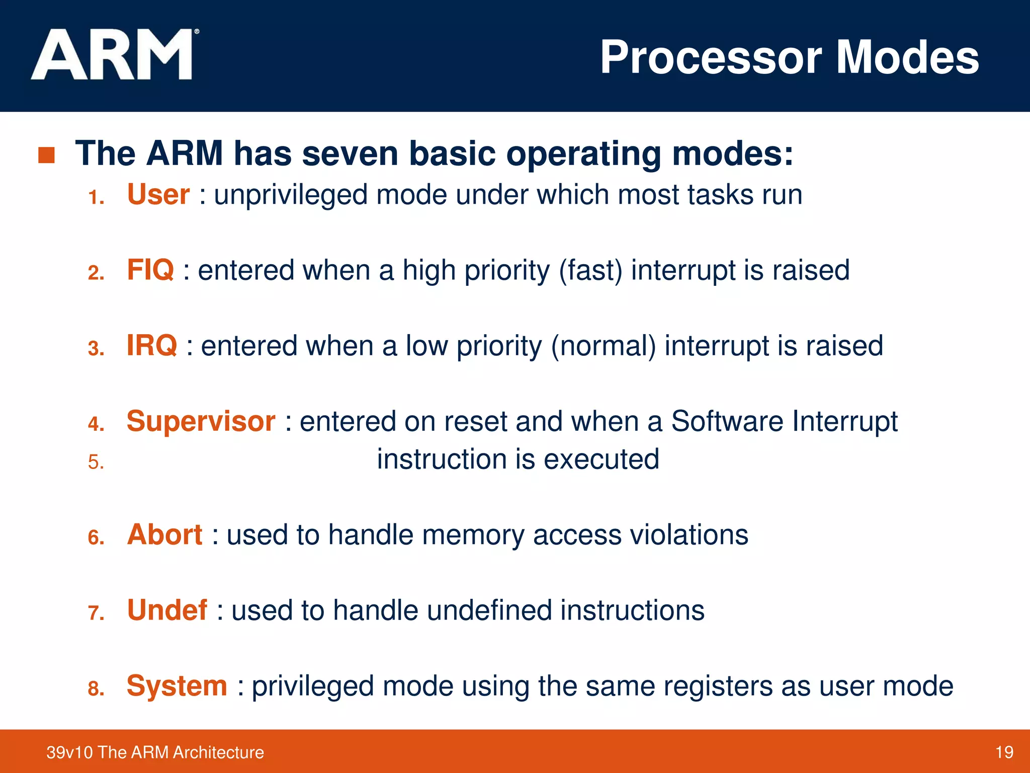
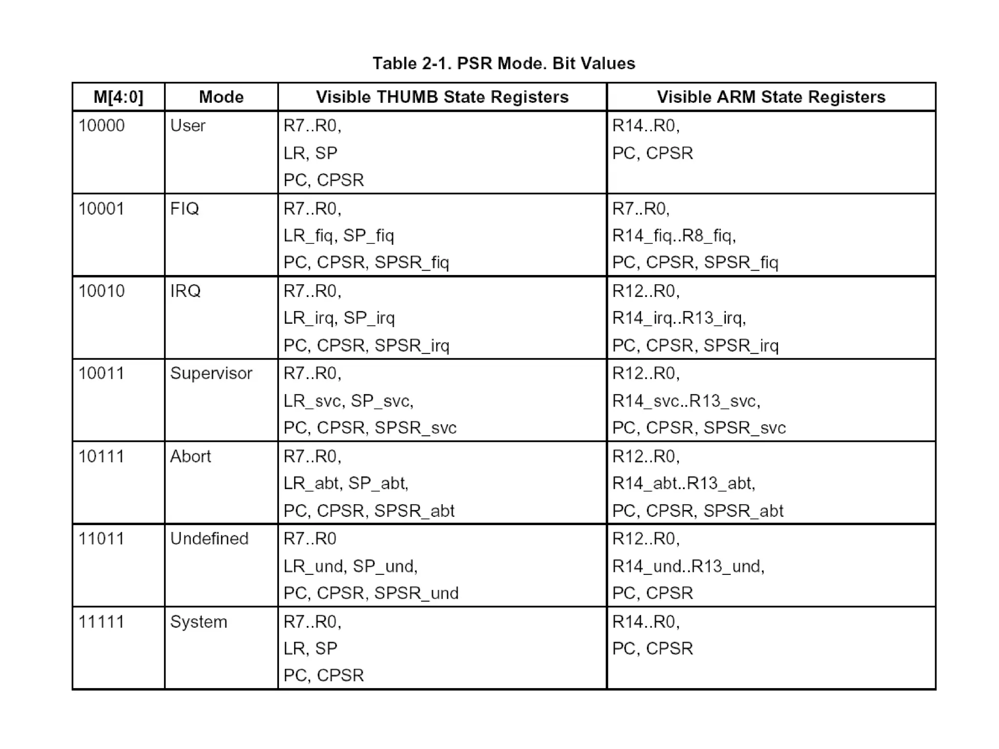
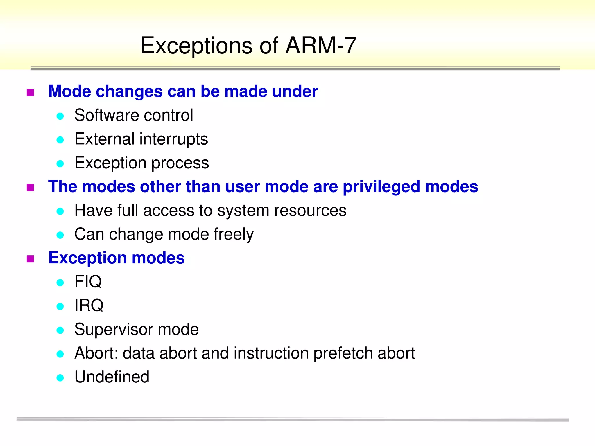
Description of the seven basic operating modes of ARM processors and their functionalities.
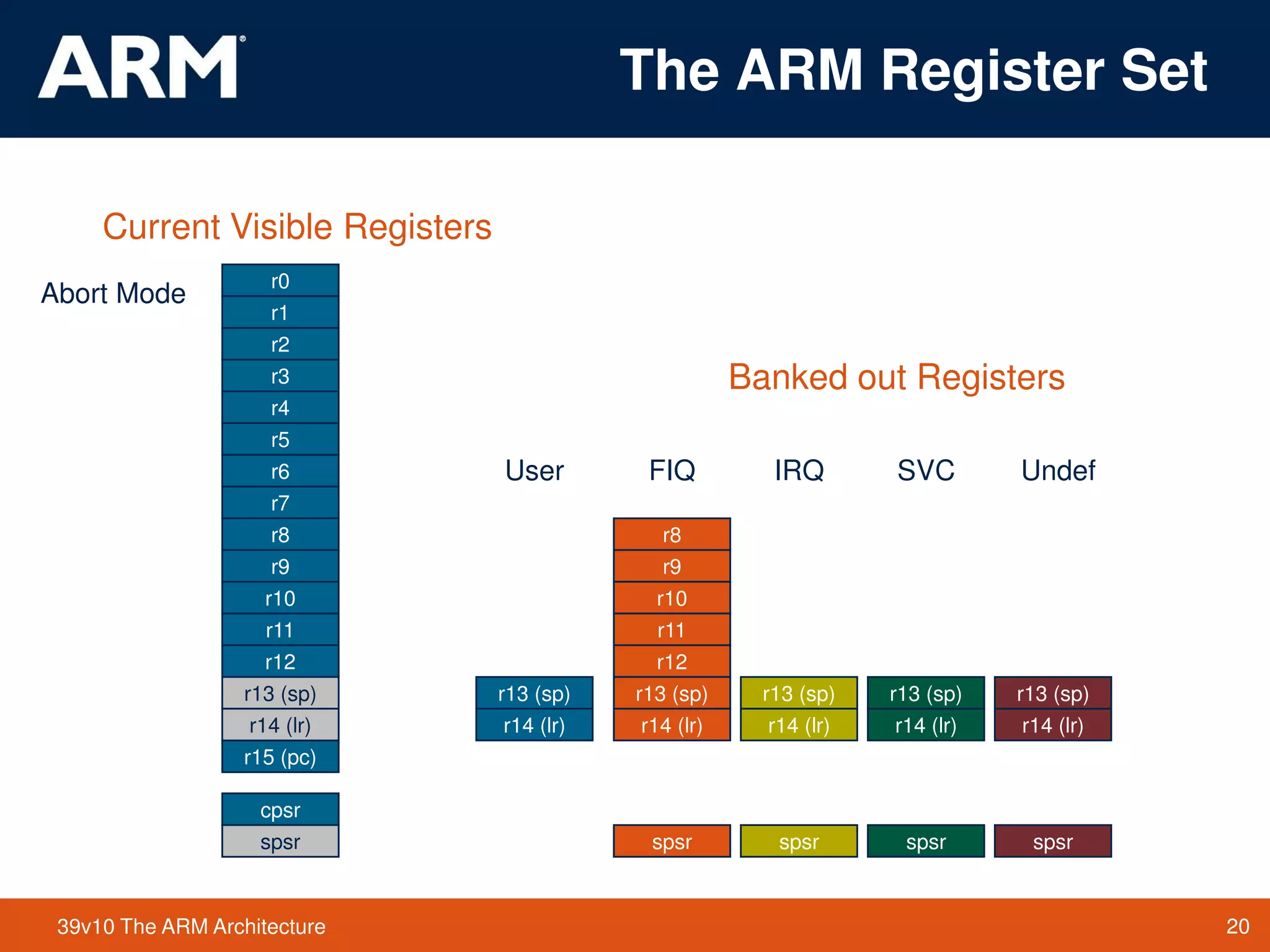
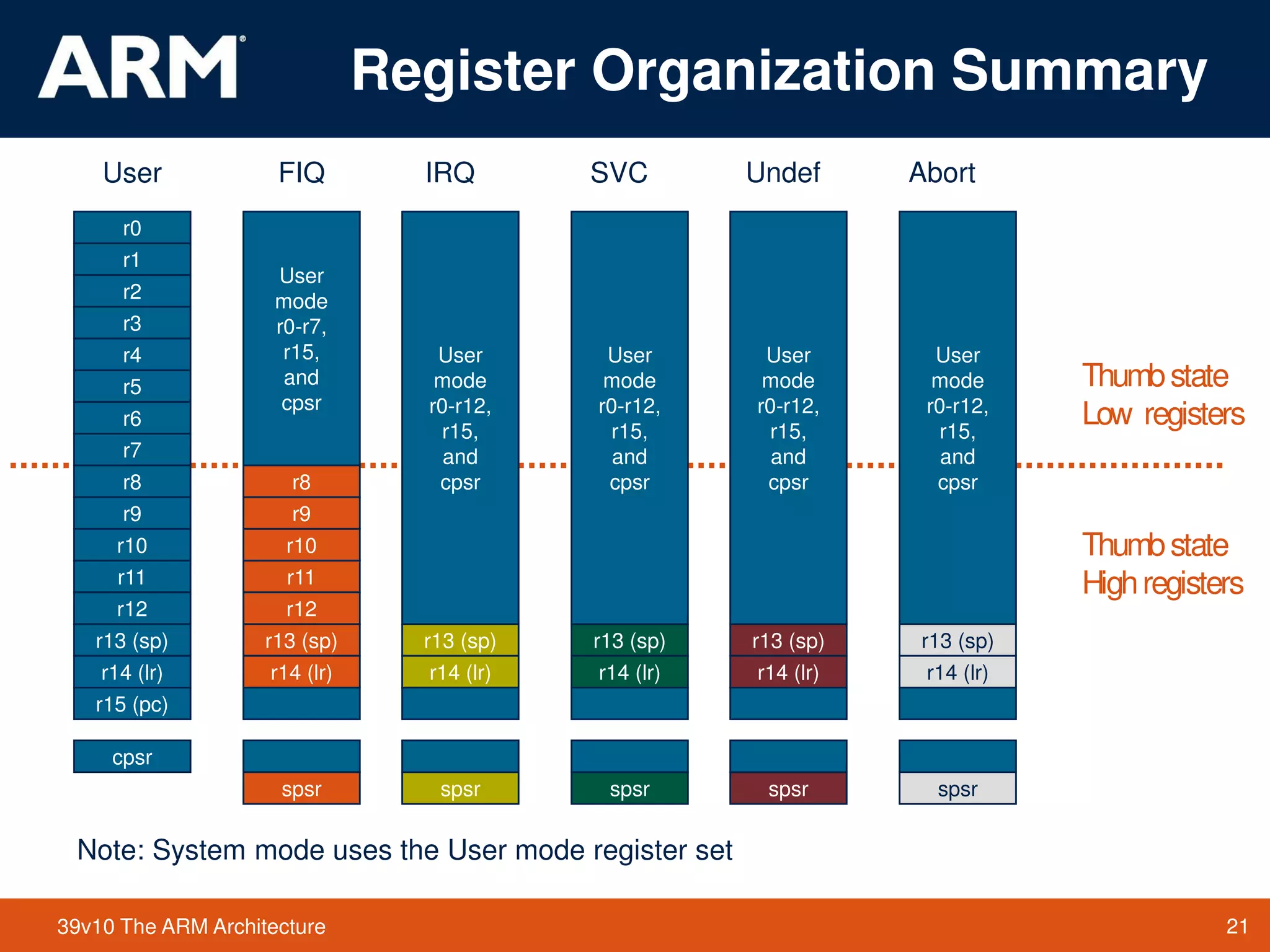
Overview of the ARM register organization, detailing general and special-purpose registers.
Summary of the ARM registers, focusing on accessibility across different modes.
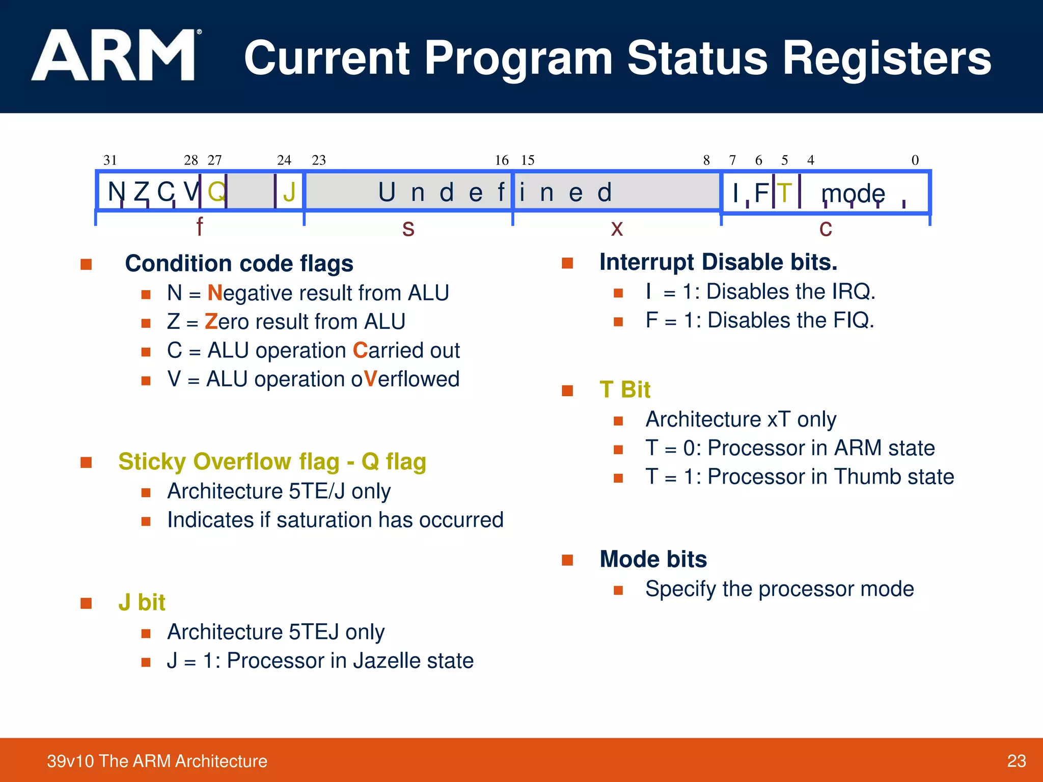
Details on current and saved program status registers and their conditions.
Examining how the program counter behavior differs between ARM and Thumb states.
The role of SPSR in preserving the CPSR state when entering a privileged mode.
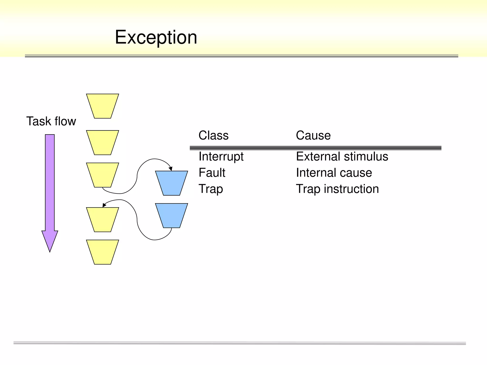
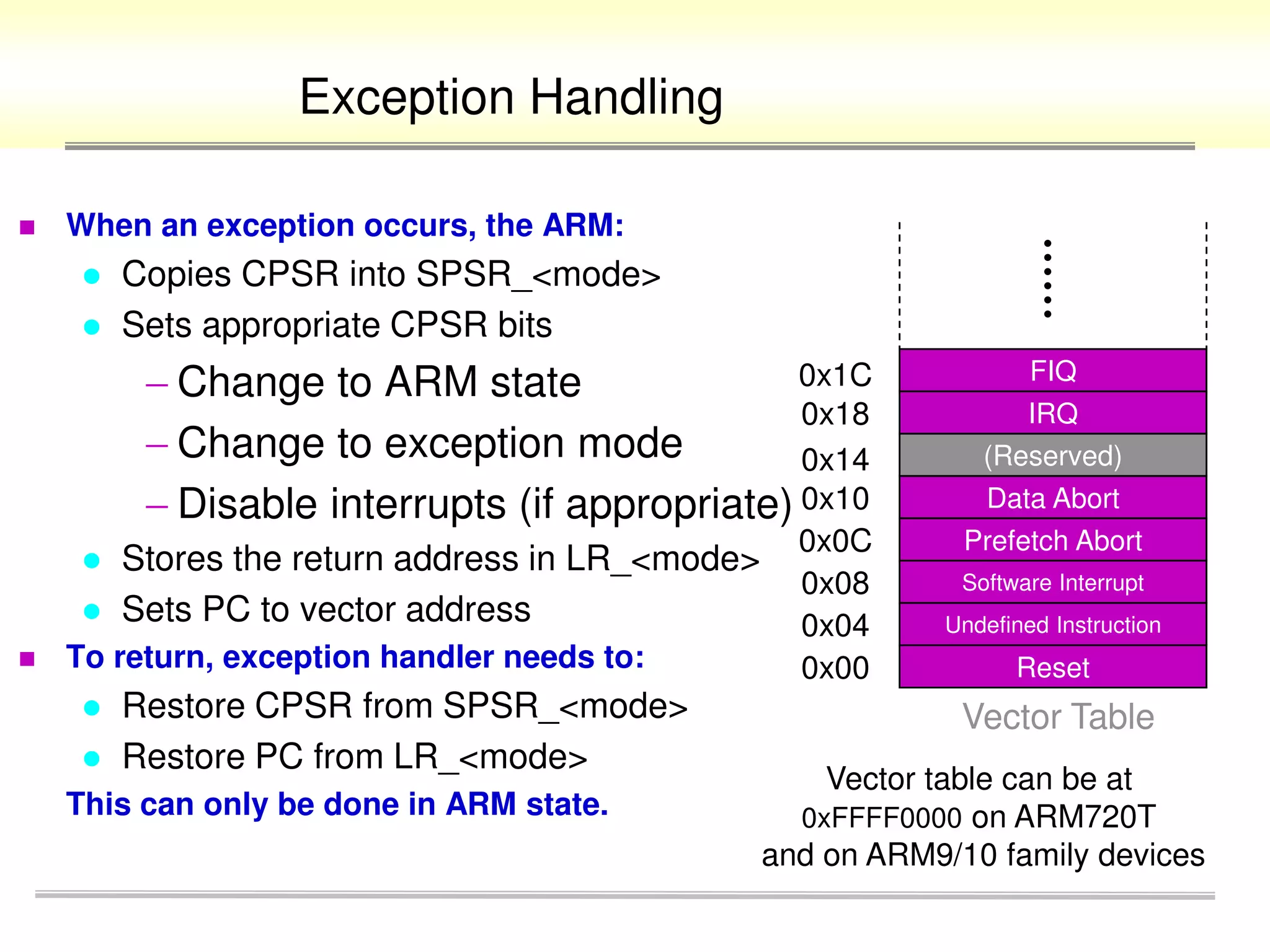
Introduction to exceptions as unexpected events during program execution.
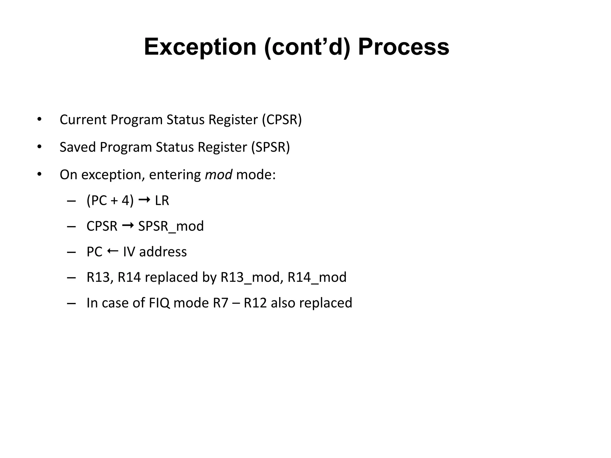
Steps the ARM processor takes to handle exceptions, changing modes and preserving state.
Processes involved in returning from an exception, restoring state.
Detailing privileged modes for exceptions and their functionality.
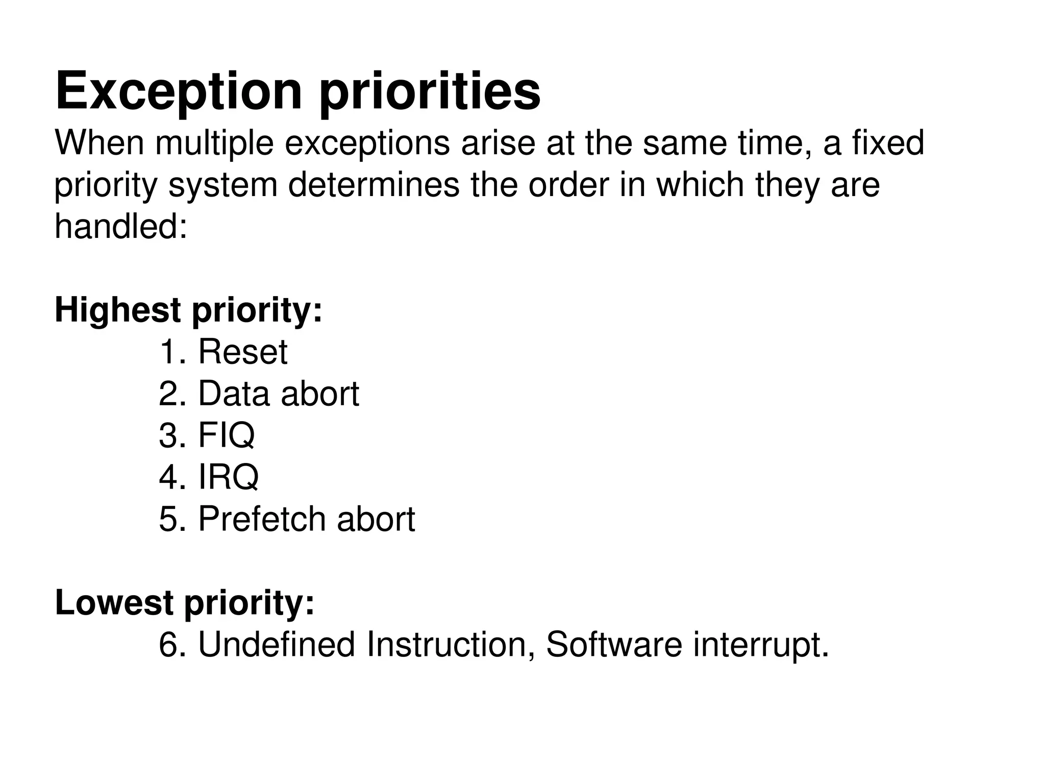
Classifying exceptions into internal and external causes.
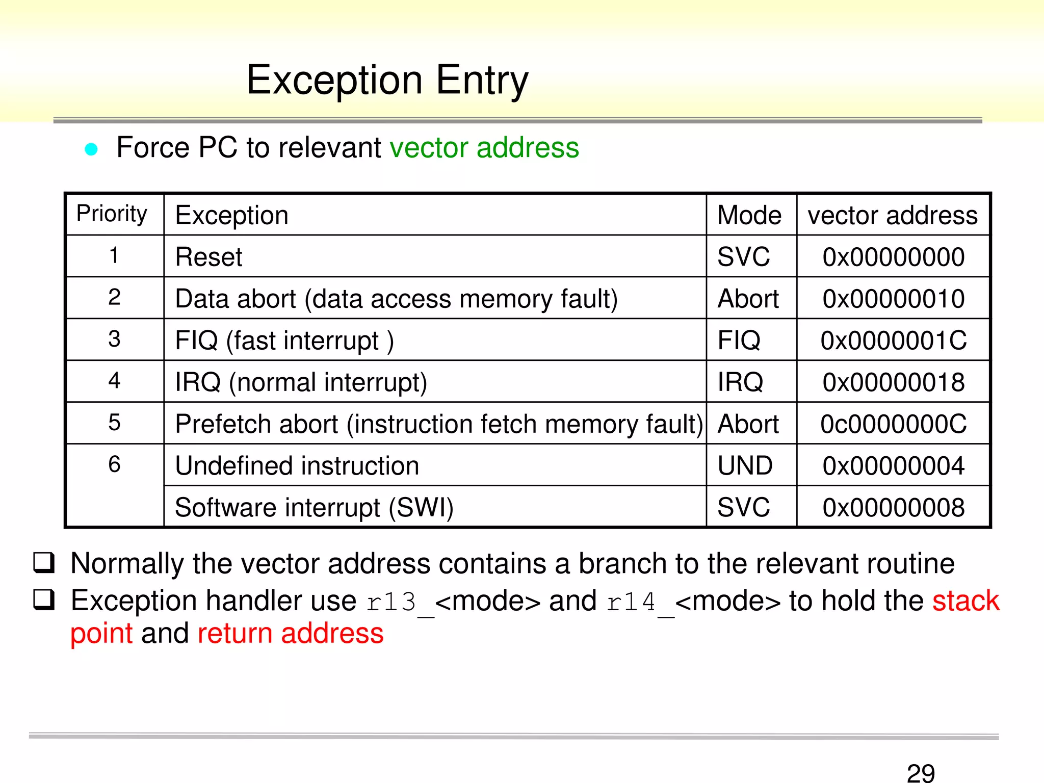
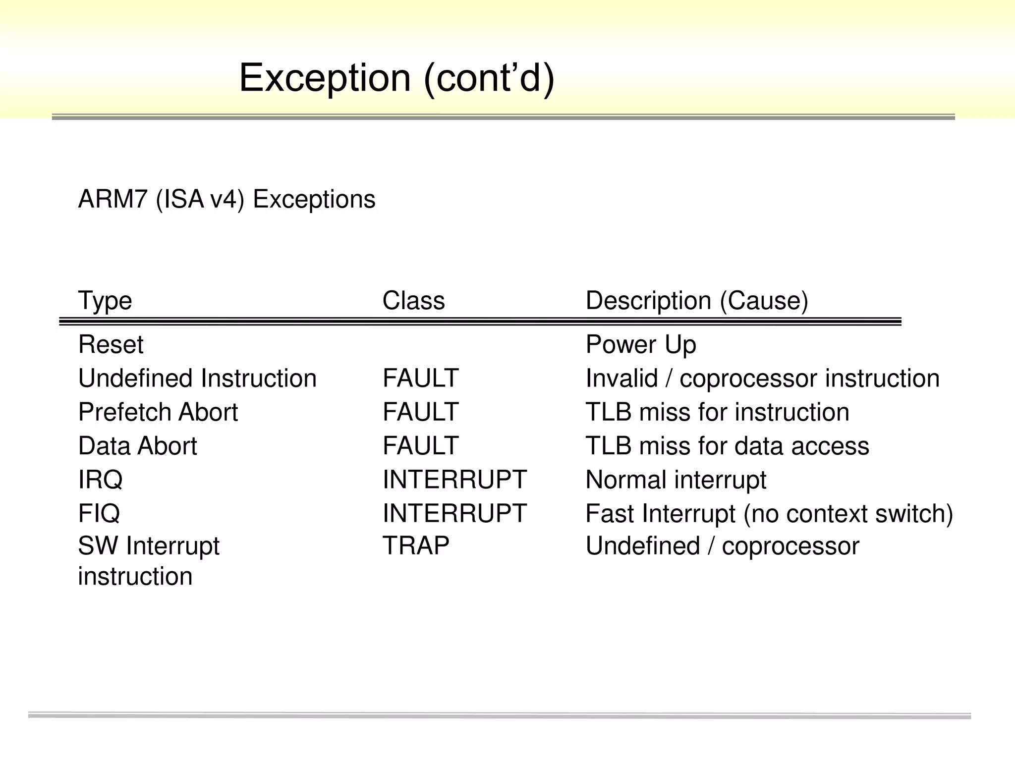
Table summarizing different ARM7 exception types including resets and faults.
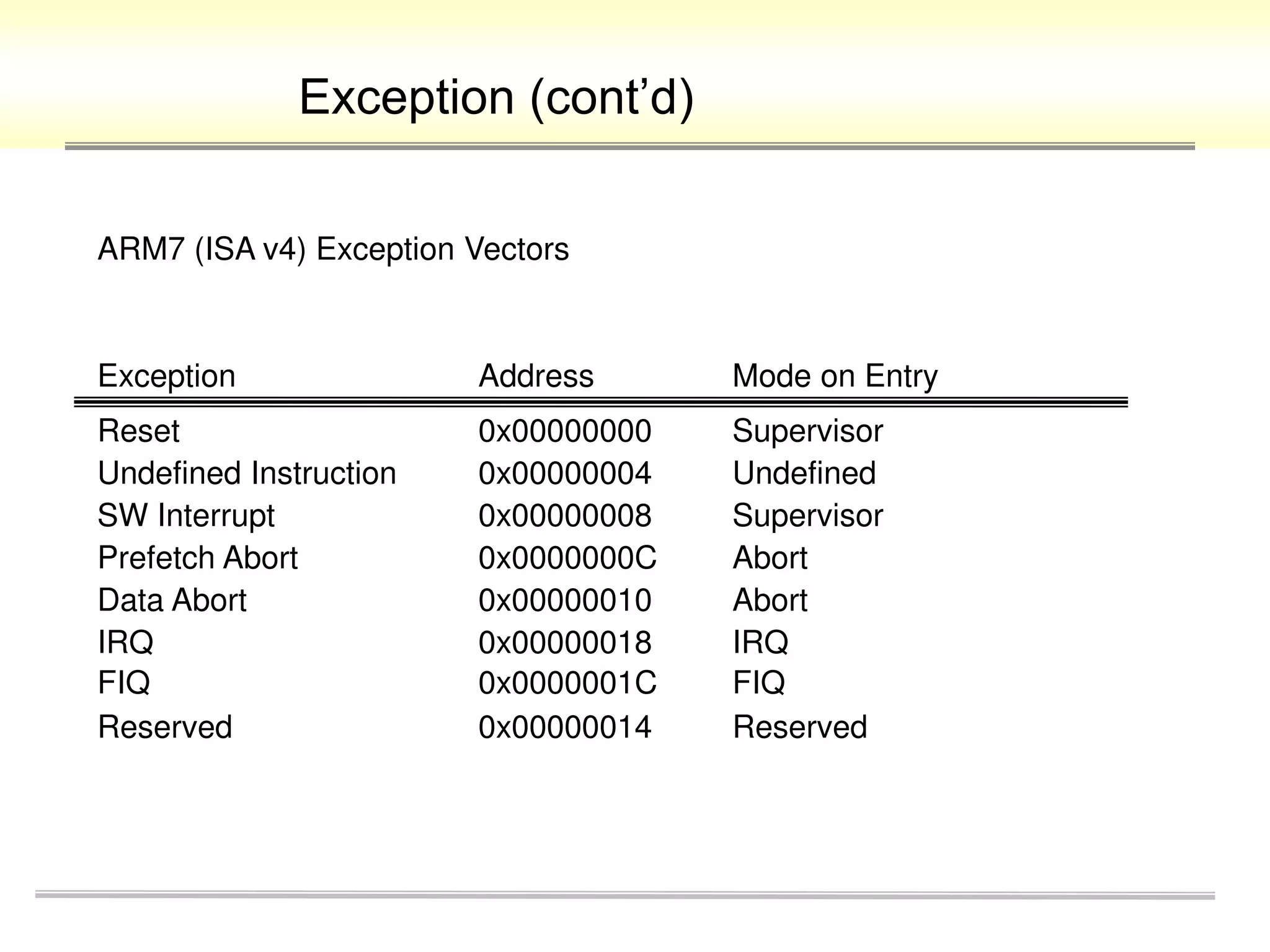
Defining memory addresses associated with each ARM exception type.
Steps the ARM processor takes upon an exception occurrence.
Behavior of the processor upon entering a mode due to exceptions.
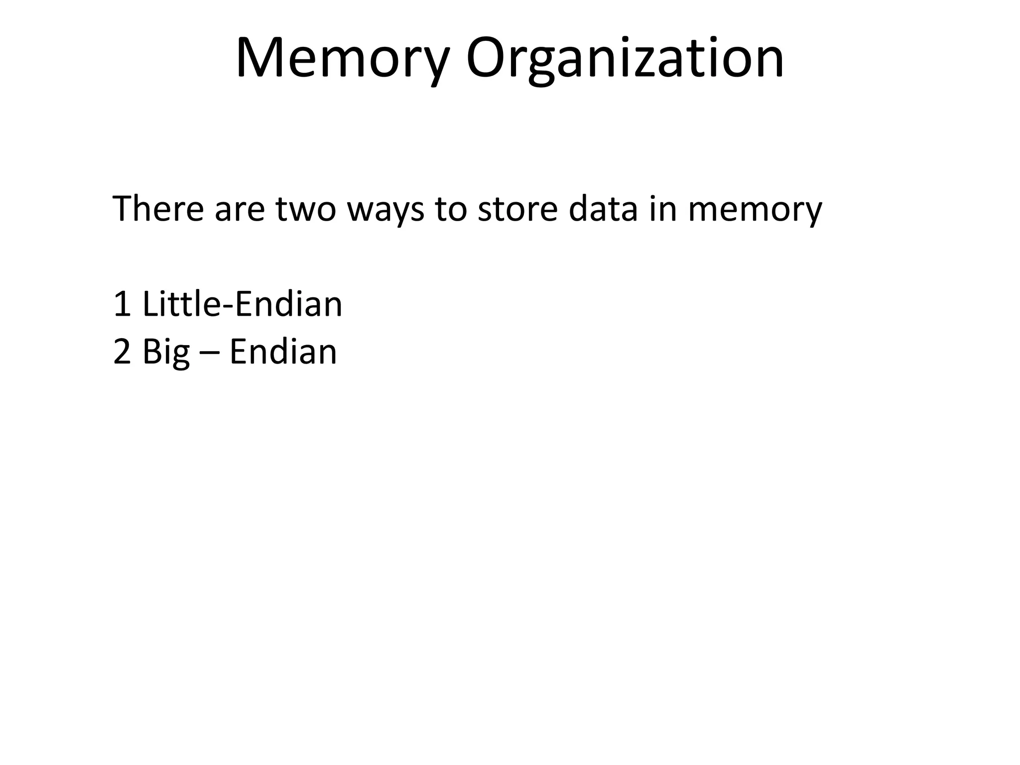
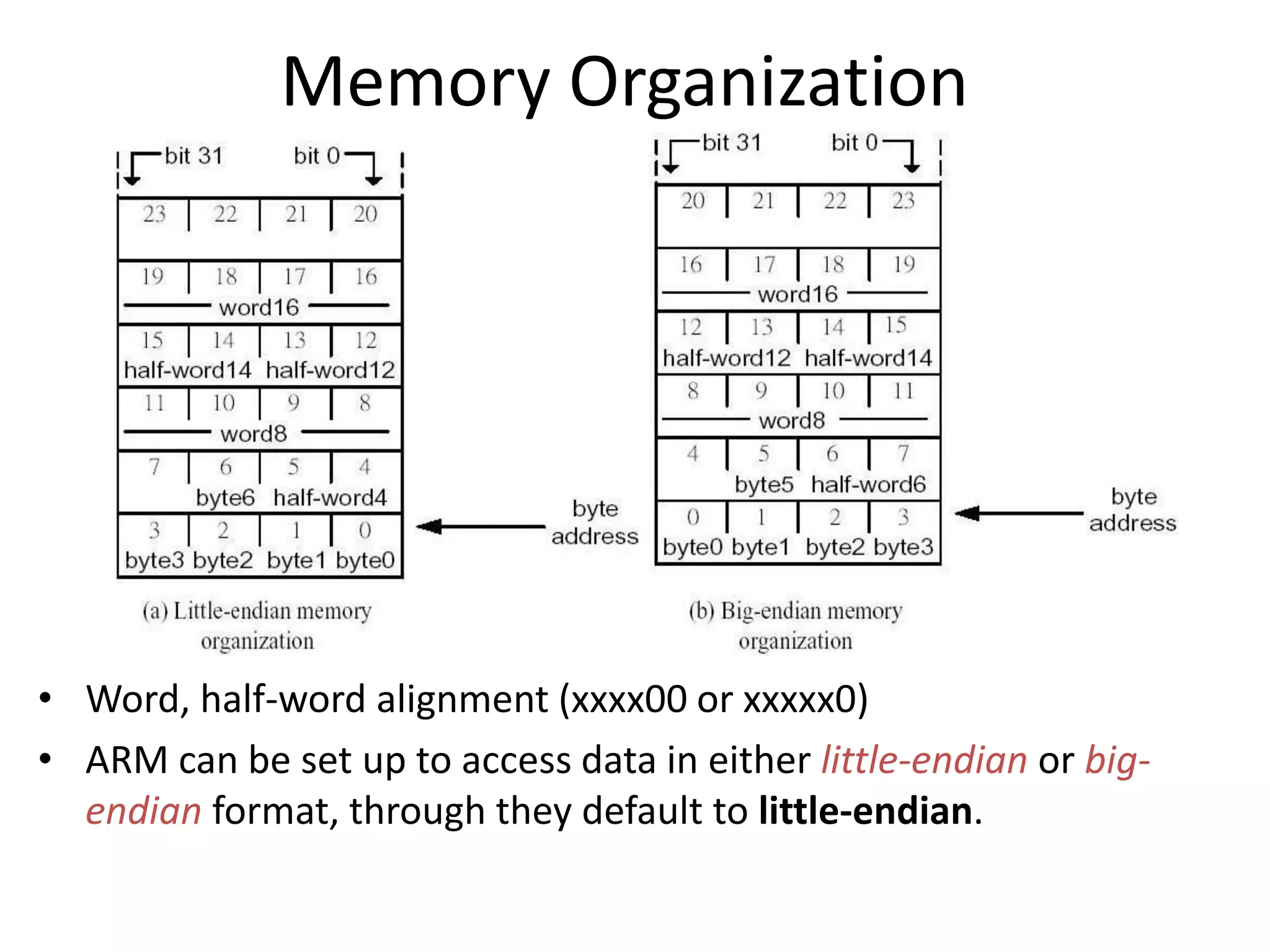
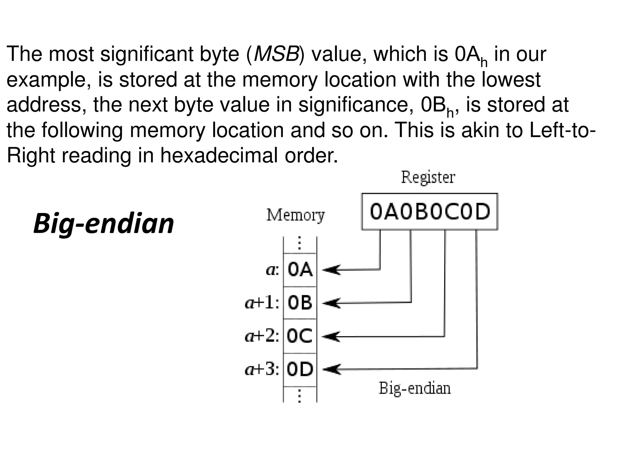
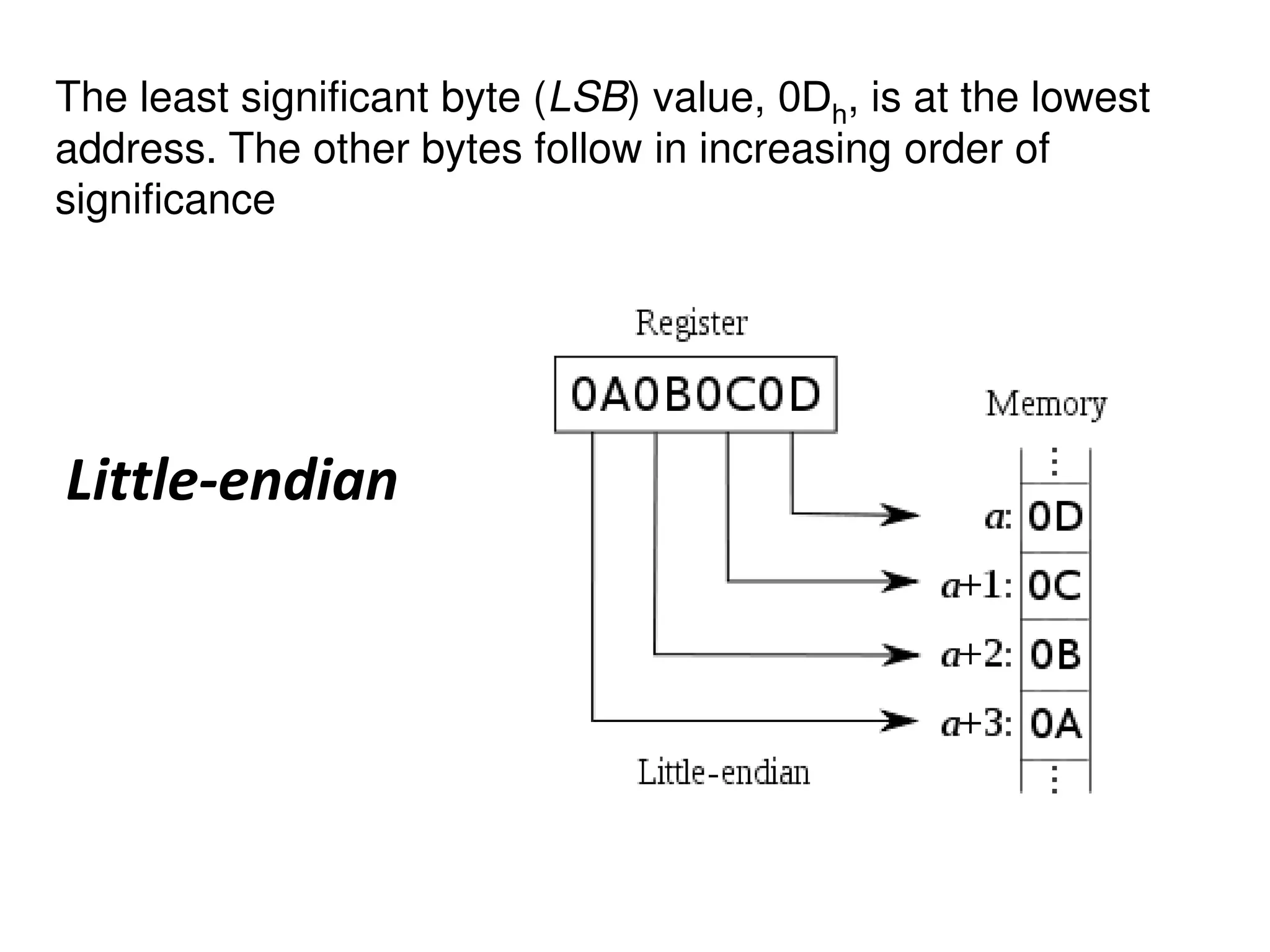
Describing two primary memory organization formats: Little-Endian and Big-Endian.
Details on memory alignment requirements for data access in ARM.
Defining how Big-Endian format organizes data in memory.
Defining how Little-Endian format organizes data in memory.
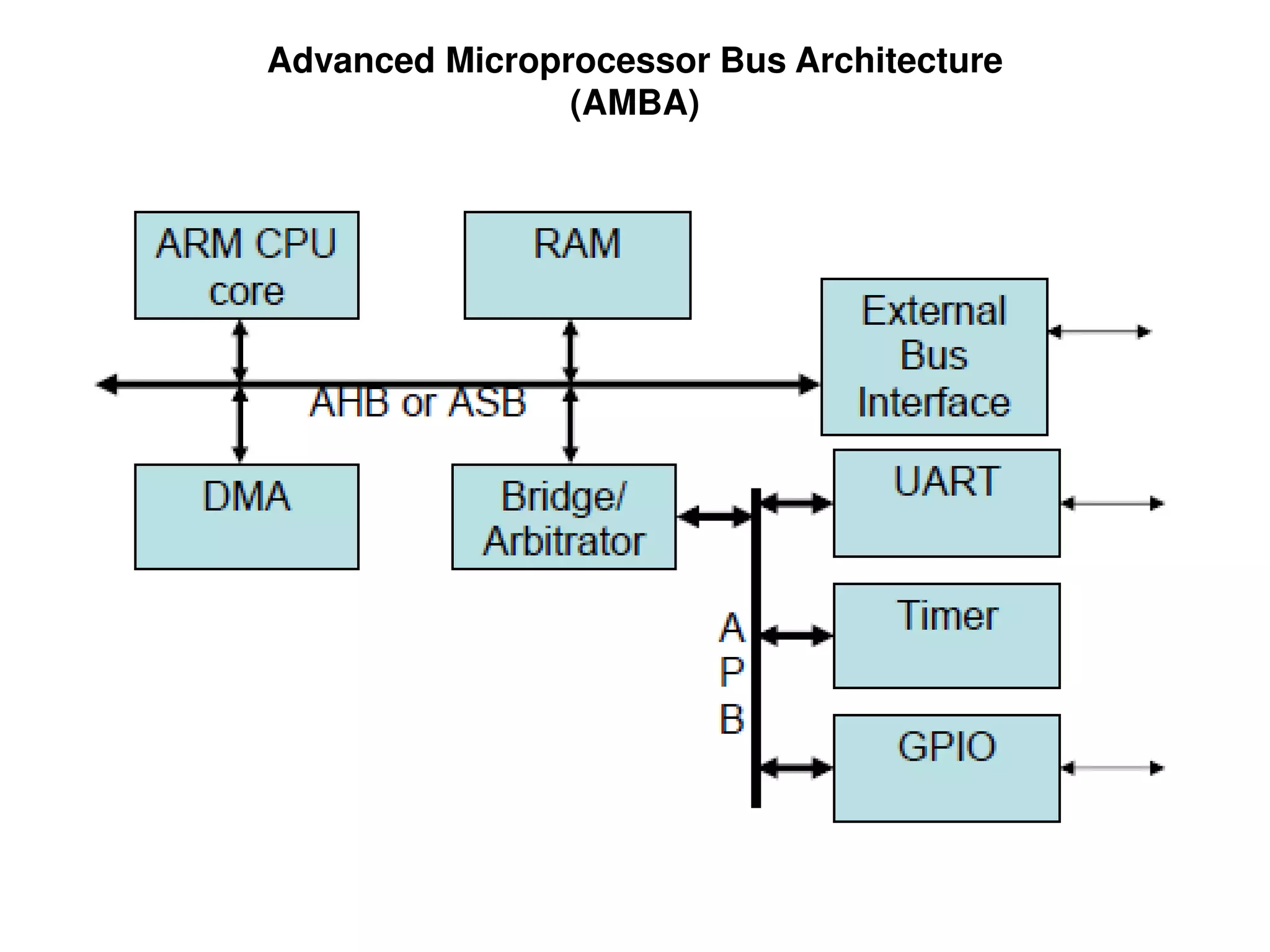
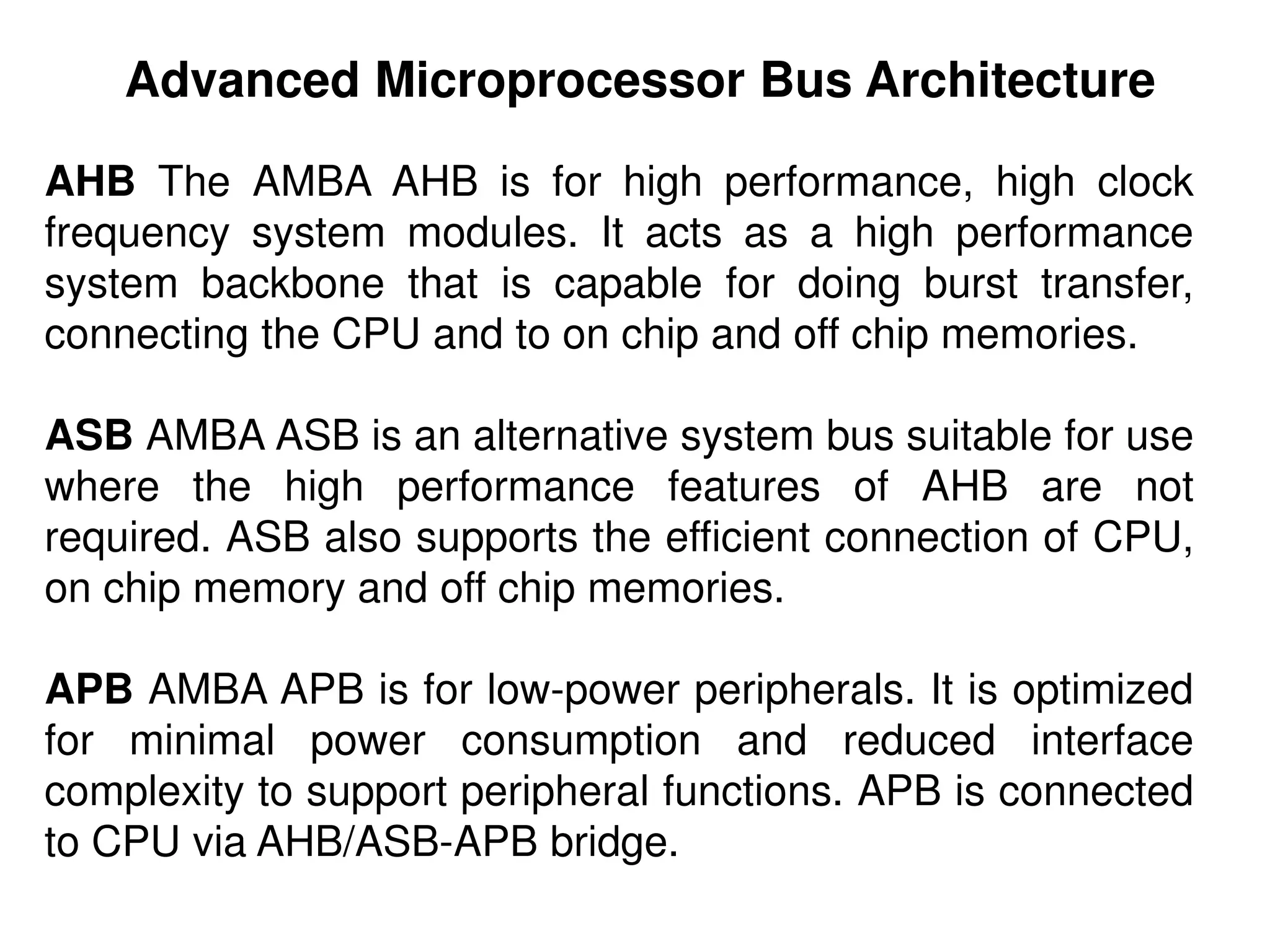
Introduction to the Advanced Microprocessor Bus Architecture (AMBA).
Overview of AMBA bus types: AHB, ASB, and APB for various performance needs.
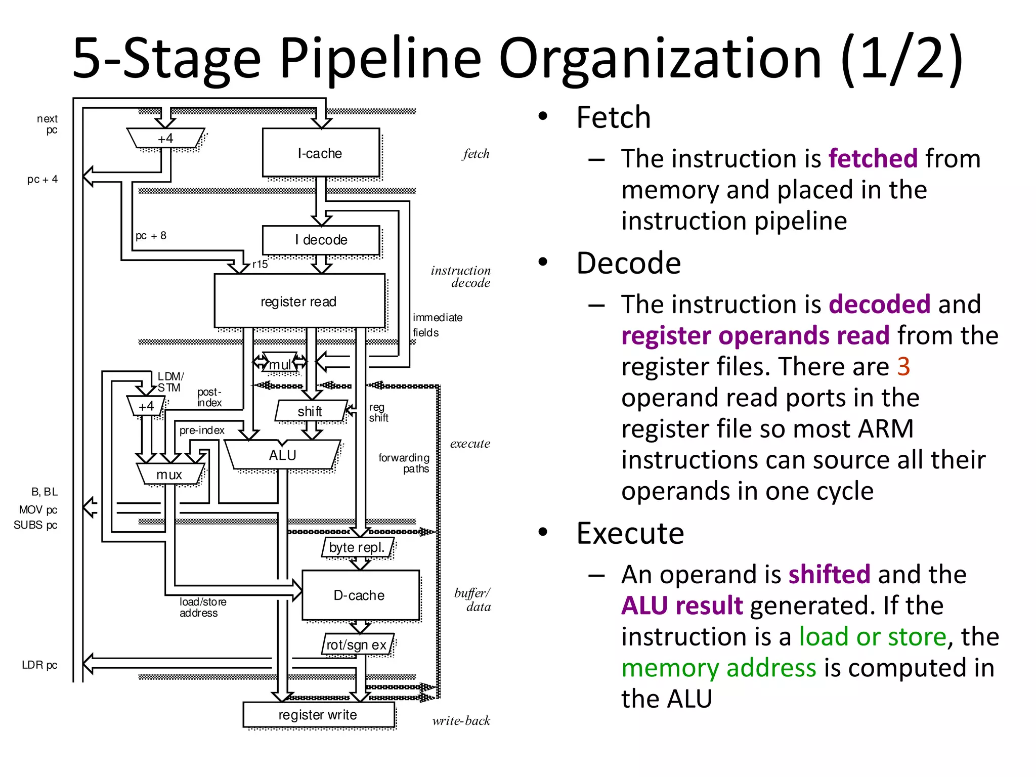
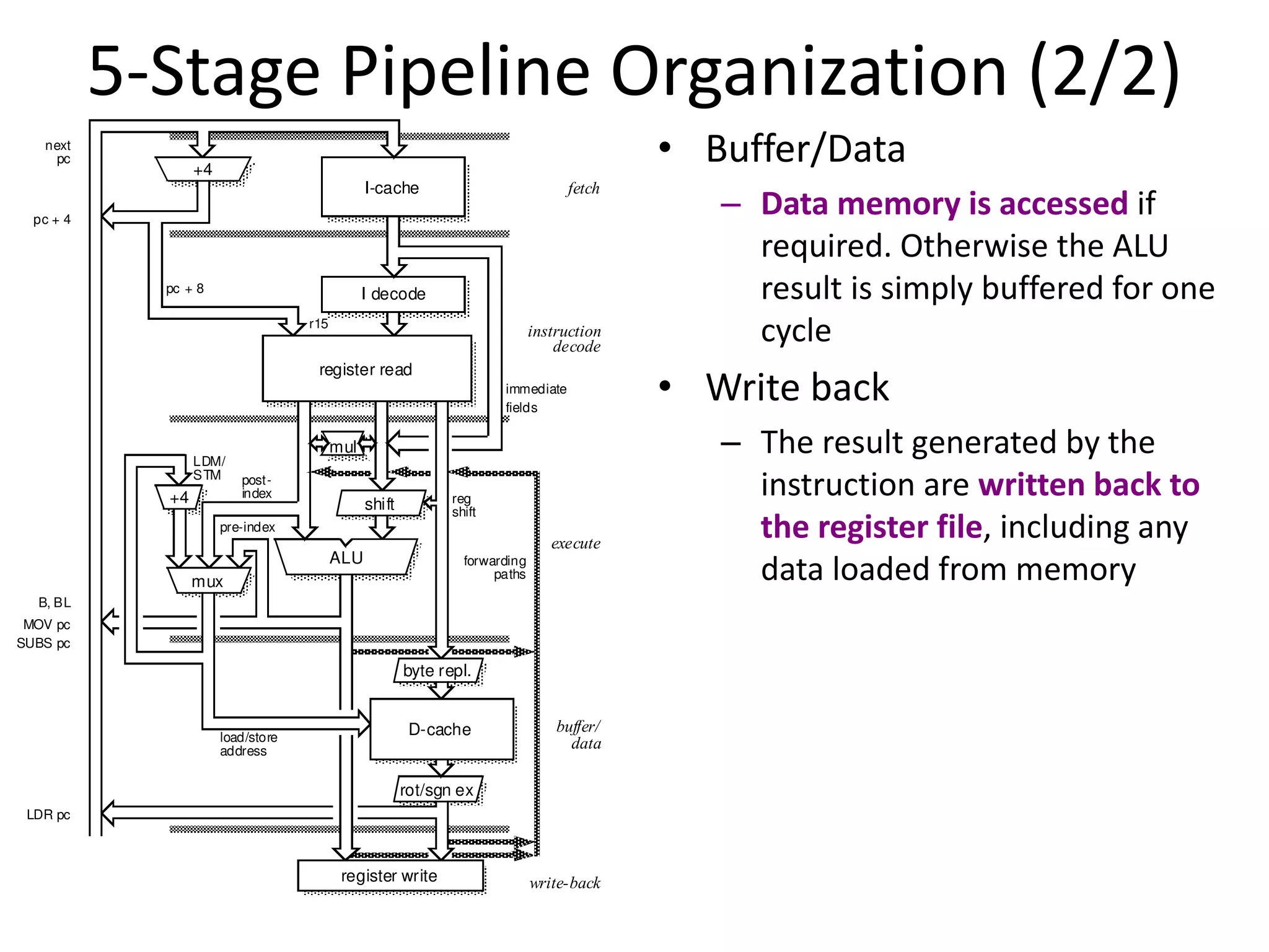
Starting overview of the ARM 5-stage pipeline design.
Explanation of how each stage of the 5-stage pipeline operates.
Further details on buffering and execution in the 5-stage pipeline.


