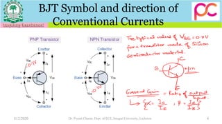
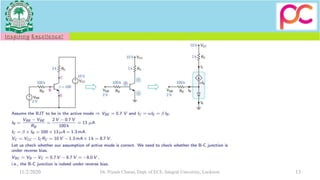
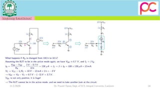
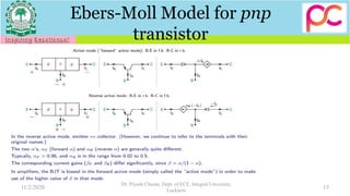
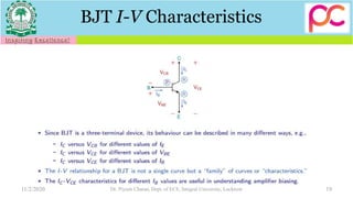
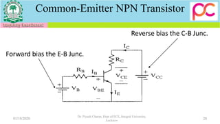
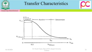
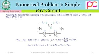
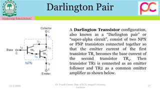
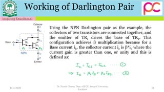
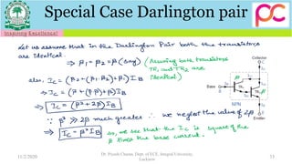
Unit 2: Bipolar Junction
Transistors (BJT)
for
Open Educational Resource
on
Electronic Devices and Circuits (EC201)
by
Dr. Piyush Charan
Assistant Professor
Department of Electronics and Communication Engg.
Integral University, Lucknow
This work is licensed under a Creative Commons Attribution-NonCommercial-ShareAlike 4.0 International License.
PNP Transistor
11/2/2020 Dr. Piyush Charan, Dept. of ECE, Integral University, Lucknow 2
In the p-n-p transistor, we have a p-
type semiconductor region followed by
an n-type region and then a p-type
region again.
NPN Transistor
11/2/2020 Dr. Piyush Charan, Dept. of ECE, Integral University, Lucknow 3
In an n-p-n transistor on the other hand,
we have an n-type region then p-type
region and again an n-type region. And in
both cases, there are three contacts
emitter, base and collector.
BJT Symbol and direction of
Conventional Currents
11/2/2020 Dr. Piyush Charan, Dept. of ECE, Integral University, Lucknow 4
Simple Numerical Example
11/2/2020 Dr. Piyush Charan, Dept. of ECE, Integral University, Lucknow 5
Q. In a certain transistor, the emitter current is 1.02 times as large as the collector
current. If the Emitter current is 12mA, find the base current.
Why BJT is called bipolar
junction transistor?
11/2/2020 Dr. Piyush Charan, Dept. of ECE, Integral University, Lucknow 6
→Bipolar because both electrons and holes contribute to conduction in these devices as
opposed to for example, MOS transistors in which only one type of carrier contributes.
→Junction, because the device includes two p-n junctions one is E-B Junction and the
other is C-B Junction. and this should be contrasted with the “point-contact” transistor
which was the first transistor to be invented by Shockley and others in 1947. This point
contact transistor is not used anymore.
→And finally, this word transistor stands for transfer resistor, and you can read more
about that at this website.
11/2/2020 Dr. Piyush Charan, Dept. of ECE, Integral University, Lucknow 7
11/2/2020 Dr. Piyush Charan, Dept. of ECE, Integral University, Lucknow 8
11/2/2020 Dr. Piyush Charan, Dept. of ECE, Integral University, Lucknow 9
11/2/2020 Dr. Piyush Charan, Dept. of ECE, Integral University, Lucknow 10
11/2/2020 Dr. Piyush Charan, Dept. of ECE, Integral University, Lucknow 11
11/2/2020 Dr. Piyush Charan, Dept. of ECE, Integral University, Lucknow 12
11/2/2020 Dr. Piyush Charan, Dept. of ECE, Integral University, Lucknow 13
11/2/2020 Dr. Piyush Charan, Dept. of ECE, Integral University, Lucknow 14
Ebers-Moll Model for pnp
transistor
11/2/2020
Dr. Piyush Charan, Dept. of ECE, Integral University,
Lucknow
15
11/2/2020 Dr. Piyush Charan, Dept. of ECE, Integral University, Lucknow 16
Ebers-Moll Model for pnp
transistor
11/2/2020 Dr. Piyush Charan, Dept. of ECE, Integral University, Lucknow 17
Ebers-Moll Model
11/2/2020 Dr. Piyush Charan, Dept. of ECE, Integral University, Lucknow 18
Ebers-Moll Model in Active Mode
11/2/2020 Dr. Piyush Charan, Dept. of ECE, Integral University, Lucknow 19
BJT I-V Characteristics
Common-Emitter NPN Transistor
01/10/2020
Dr. Piyush Charan, Dept of ECE, Integral University,
Lucknow
20
Forward bias the E-B Junc.
Reverse bias the C-B Junc.
Input Characteristics
• Plot IB as f(VBE, VCE)
• As VCE increases, more
VBE required to turn the
BE on so that IB>0.
• Looks like a p-n junction
volt-ampere characteristic.
01/10/2020
Dr. Piyush Charan, Dept of ECE, Integral
University, Lucknow
21
Output Characteristics
• Plot IC as f(VCE, IB)
• Cutoff region (off)
– both BE and BC reverse
biased
• Active region
– BE Forward biased
– BC Reverse biased
• Saturation region (on)
– both BE and BC forward
biased
01/10/2020
Dr. Piyush Charan, Dept of ECE, Integral
University, Lucknow
22
Transfer Characteristics
01/10/2020
Dr. Piyush Charan, Dept of ECE, Integral University,
Lucknow
23
11/2/2020 Dr. Piyush Charan, Dept. of ECE, Integral University, Lucknow 24
Numerical Problem 1: Simple
BJT Circuit
11/2/2020 Dr. Piyush Charan, Dept. of ECE, Integral University, Lucknow 25
Numerical Problem 1: Continued……..
Darlington Pair Amplifier
11/2/2020
Dr. Piyush Charan, Dept. of ECE, Integral University,
Lucknow
26
A Darlington transistor acts as a single
transistor with high current gain, it means
that a small amount of current is used from
a microcontroller or a sensor to run a
larger load. For instance, the following
circuit is explained below. The Darlington
circuit is built with two transistors shown
in the circuit diagram, alongside.
Darlington Pair
11/2/2020
Dr. Piyush Charan, Dept. of ECE, Integral University,
Lucknow
27
A Darlington Transistor configuration,
also known as a “Darlington pair” or
“super-alpha circuit”, consist of two NPN
or PNP transistors connected together so
that the emitter current of the first
transistor TR1 becomes the base current of
the second transistor TR2. Then
transistor TR1 is connected as an emitter
follower and TR2 as a common emitter
amplifier as shown below.
Working of Darlington Pair
11/2/2020
Dr. Piyush Charan, Dept. of ECE, Integral University,
Lucknow
28
Using the NPN Darlington pair as the example, the
collectors of two transistors are connected together, and
the emitter of TR1 drives the base of TR2. This
configuration achieves β multiplication because for a
Base current ib, the collector current ic is β*ib where the
current gain is greater than one, or unity and this is
defined as:
DP working contd…
11/2/2020
Dr. Piyush Charan, Dept. of ECE, Integral University,
Lucknow
29
But the base current, IB2 is equal to transistor TR1 emitter current, IE1 as the emitter of TR1 is
connected to the base of TR2. Therefore:
Then substituting in the equation 2 :
Where β1 and β2 are the gains of the individual transistors.
DP working contd…
11/2/2020
Dr. Piyush Charan, Dept. of ECE, Integral University,
Lucknow
30
This means that the overall current gain, β is given by the gain of the first
transistor multiplied by the gain of the second transistor as the current gains of
the two transistors multiply.
In other words, a pair of bipolar transistors combined together to make a single
Darlington transistor pair can be regarded as a single transistor with a very high
value of β and consequently a high input resistance.
Numerical on Darlington Pair
11/2/2020
Dr. Piyush Charan, Dept. of ECE, Integral University,
Lucknow
31
❖ Q1. Two NPN transistors are connected together in the form of a Darlington Pair to
switch a 12V 75W halogen lamp. If the forward current gain (β1)of the first transistor is 25 and
the forward current gain (β2) of the second transistor is 80. Ignoring any voltage drops across
the two transistors, calculate the maximum base current required to switch the lamp fully-ON.
Numerical on Darlington Pair
contd…
11/2/2020
Dr. Piyush Charan, Dept. of ECE, Integral University,
Lucknow
32
Special Case Darlington pair
11/2/2020
Dr. Piyush Charan, Dept. of ECE, Integral University,
Lucknow
33

Unit 2 bjt notes

  • 1.
    Unit 2: BipolarJunction Transistors (BJT) for Open Educational Resource on Electronic Devices and Circuits (EC201) by Dr. Piyush Charan Assistant Professor Department of Electronics and Communication Engg. Integral University, Lucknow This work is licensed under a Creative Commons Attribution-NonCommercial-ShareAlike 4.0 International License.
  • 2.
    PNP Transistor 11/2/2020 Dr.Piyush Charan, Dept. of ECE, Integral University, Lucknow 2 In the p-n-p transistor, we have a p- type semiconductor region followed by an n-type region and then a p-type region again.
  • 3.
    NPN Transistor 11/2/2020 Dr.Piyush Charan, Dept. of ECE, Integral University, Lucknow 3 In an n-p-n transistor on the other hand, we have an n-type region then p-type region and again an n-type region. And in both cases, there are three contacts emitter, base and collector.
  • 4.
    BJT Symbol anddirection of Conventional Currents 11/2/2020 Dr. Piyush Charan, Dept. of ECE, Integral University, Lucknow 4
  • 5.
    Simple Numerical Example 11/2/2020Dr. Piyush Charan, Dept. of ECE, Integral University, Lucknow 5 Q. In a certain transistor, the emitter current is 1.02 times as large as the collector current. If the Emitter current is 12mA, find the base current.
  • 6.
    Why BJT iscalled bipolar junction transistor? 11/2/2020 Dr. Piyush Charan, Dept. of ECE, Integral University, Lucknow 6 →Bipolar because both electrons and holes contribute to conduction in these devices as opposed to for example, MOS transistors in which only one type of carrier contributes. →Junction, because the device includes two p-n junctions one is E-B Junction and the other is C-B Junction. and this should be contrasted with the “point-contact” transistor which was the first transistor to be invented by Shockley and others in 1947. This point contact transistor is not used anymore. →And finally, this word transistor stands for transfer resistor, and you can read more about that at this website.
  • 7.
    11/2/2020 Dr. PiyushCharan, Dept. of ECE, Integral University, Lucknow 7
  • 8.
    11/2/2020 Dr. PiyushCharan, Dept. of ECE, Integral University, Lucknow 8
  • 9.
    11/2/2020 Dr. PiyushCharan, Dept. of ECE, Integral University, Lucknow 9
  • 10.
    11/2/2020 Dr. PiyushCharan, Dept. of ECE, Integral University, Lucknow 10
  • 11.
    11/2/2020 Dr. PiyushCharan, Dept. of ECE, Integral University, Lucknow 11
  • 12.
    11/2/2020 Dr. PiyushCharan, Dept. of ECE, Integral University, Lucknow 12
  • 13.
    11/2/2020 Dr. PiyushCharan, Dept. of ECE, Integral University, Lucknow 13
  • 14.
    11/2/2020 Dr. PiyushCharan, Dept. of ECE, Integral University, Lucknow 14
  • 15.
    Ebers-Moll Model forpnp transistor 11/2/2020 Dr. Piyush Charan, Dept. of ECE, Integral University, Lucknow 15
  • 16.
    11/2/2020 Dr. PiyushCharan, Dept. of ECE, Integral University, Lucknow 16 Ebers-Moll Model for pnp transistor
  • 17.
    11/2/2020 Dr. PiyushCharan, Dept. of ECE, Integral University, Lucknow 17 Ebers-Moll Model
  • 18.
    11/2/2020 Dr. PiyushCharan, Dept. of ECE, Integral University, Lucknow 18 Ebers-Moll Model in Active Mode
  • 19.
    11/2/2020 Dr. PiyushCharan, Dept. of ECE, Integral University, Lucknow 19 BJT I-V Characteristics
  • 20.
    Common-Emitter NPN Transistor 01/10/2020 Dr.Piyush Charan, Dept of ECE, Integral University, Lucknow 20 Forward bias the E-B Junc. Reverse bias the C-B Junc.
  • 21.
    Input Characteristics • PlotIB as f(VBE, VCE) • As VCE increases, more VBE required to turn the BE on so that IB>0. • Looks like a p-n junction volt-ampere characteristic. 01/10/2020 Dr. Piyush Charan, Dept of ECE, Integral University, Lucknow 21
  • 22.
    Output Characteristics • PlotIC as f(VCE, IB) • Cutoff region (off) – both BE and BC reverse biased • Active region – BE Forward biased – BC Reverse biased • Saturation region (on) – both BE and BC forward biased 01/10/2020 Dr. Piyush Charan, Dept of ECE, Integral University, Lucknow 22
  • 23.
    Transfer Characteristics 01/10/2020 Dr. PiyushCharan, Dept of ECE, Integral University, Lucknow 23
  • 24.
    11/2/2020 Dr. PiyushCharan, Dept. of ECE, Integral University, Lucknow 24 Numerical Problem 1: Simple BJT Circuit
  • 25.
    11/2/2020 Dr. PiyushCharan, Dept. of ECE, Integral University, Lucknow 25 Numerical Problem 1: Continued……..
  • 26.
    Darlington Pair Amplifier 11/2/2020 Dr.Piyush Charan, Dept. of ECE, Integral University, Lucknow 26 A Darlington transistor acts as a single transistor with high current gain, it means that a small amount of current is used from a microcontroller or a sensor to run a larger load. For instance, the following circuit is explained below. The Darlington circuit is built with two transistors shown in the circuit diagram, alongside.
  • 27.
    Darlington Pair 11/2/2020 Dr. PiyushCharan, Dept. of ECE, Integral University, Lucknow 27 A Darlington Transistor configuration, also known as a “Darlington pair” or “super-alpha circuit”, consist of two NPN or PNP transistors connected together so that the emitter current of the first transistor TR1 becomes the base current of the second transistor TR2. Then transistor TR1 is connected as an emitter follower and TR2 as a common emitter amplifier as shown below.
  • 28.
    Working of DarlingtonPair 11/2/2020 Dr. Piyush Charan, Dept. of ECE, Integral University, Lucknow 28 Using the NPN Darlington pair as the example, the collectors of two transistors are connected together, and the emitter of TR1 drives the base of TR2. This configuration achieves β multiplication because for a Base current ib, the collector current ic is β*ib where the current gain is greater than one, or unity and this is defined as:
  • 29.
    DP working contd… 11/2/2020 Dr.Piyush Charan, Dept. of ECE, Integral University, Lucknow 29 But the base current, IB2 is equal to transistor TR1 emitter current, IE1 as the emitter of TR1 is connected to the base of TR2. Therefore: Then substituting in the equation 2 : Where β1 and β2 are the gains of the individual transistors.
  • 30.
    DP working contd… 11/2/2020 Dr.Piyush Charan, Dept. of ECE, Integral University, Lucknow 30 This means that the overall current gain, β is given by the gain of the first transistor multiplied by the gain of the second transistor as the current gains of the two transistors multiply. In other words, a pair of bipolar transistors combined together to make a single Darlington transistor pair can be regarded as a single transistor with a very high value of β and consequently a high input resistance.
  • 31.
    Numerical on DarlingtonPair 11/2/2020 Dr. Piyush Charan, Dept. of ECE, Integral University, Lucknow 31 ❖ Q1. Two NPN transistors are connected together in the form of a Darlington Pair to switch a 12V 75W halogen lamp. If the forward current gain (β1)of the first transistor is 25 and the forward current gain (β2) of the second transistor is 80. Ignoring any voltage drops across the two transistors, calculate the maximum base current required to switch the lamp fully-ON.
  • 32.
    Numerical on DarlingtonPair contd… 11/2/2020 Dr. Piyush Charan, Dept. of ECE, Integral University, Lucknow 32
  • 33.
    Special Case Darlingtonpair 11/2/2020 Dr. Piyush Charan, Dept. of ECE, Integral University, Lucknow 33