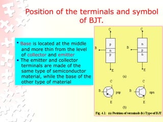
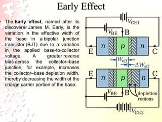
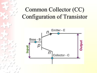
Bipolar Junction Transistor
(BJT)
(BJT)
UNIT 5
Introduction
Introduction
• The basic of electronic system nowadays is
semiconductor device.
• The famous and commonly use of this device is BJTs
(Bipolar Junction Transistors).
• It can be use as amplifier and logic switches.
• BJT consists of three terminal:
 collector : C
 base : B
emitter : E
• Two types of BJT : pnp and npn
Transistor Construction
• 3 layer semiconductor device consisting:
• 2 n- and 1 p-type layers of material  npn transistor
• 2 p- and 1 n-type layers of material pnp transistor
• The term bipolar reflects the fact that holes and electrons
participate in the injection process into the oppositely polarized
material
• A single pn junction has two different types of bias:
• forward bias
• reverse bias
• Thus, a two-pn-junction device has four types of bias.
Position of the terminals and symbol
of BJT.
• Base is located at the middle
and more thin from the level
of collector and emitter
• The emitter and collector
terminals are made of the
same type of semiconductor
material, while the base of the
other type of material
Transistor currents
-The arrow is always drawn
on the emitter
-The arrow always point
toward the n-type
-The arrow indicates the
direction of the emitter
current:
pnp:E B
npn: B E
IC=the collector current
IB= the base current
IE= the emitter current
• By imaging the analogy of diode, transistor can be
construct like two diodes that connetecd together.
• It can be conclude that the work of transistor is base on
work of diode.
Transistor Operation
• The basic operation will be described using the pnp
transistor. The operation of the pnp transistor is
exactly the same if the roles played by the electron
and hole are interchanged.
• One p-n junction of a transistor is reverse-biased,
whereas the other is forward-biased.
Forward-biased junction
of a pnp transistor
Reverse-biased junction
of a pnp transistor
• Both biasing potentials have been applied to a pnp
transistor and resulting majority and minority carrier flows
indicated.
• Majority carriers (+) will diffuse across the forward-biased
p-n junction into the n-type material.
• A very small number of carriers (+) will through n-type
material to the base terminal. Resulting IB is typically in
order of microamperes.
• The large number of majority carriers will diffuse across the
reverse-biased junction into the p-type material connected
to the collector terminal.
• Majority carriers can cross the reverse-biased
junction because the injected majority carriers will
appear as minority carriers in the n-type material.
• Applying KCL to the transistor :
IE = IC + IB
• The comprises of two components – the majority
and minority carriers
IC = ICmajority + ICOminority
• ICO – IC current with emitter terminal open and is
called leakage current.
Ebers-Moll Model
• A good, functional model of the BJT is the simplified
Ebers-Moll model. This utilizes an ideal diode to model
the base-emitter junction and a current-controlled current
source located at the collector-base. This model is
sufficient to achieve good analysis results with a variety
of DC and low frequency circuits. It is important to
remember, though, that β varies not only from device to
device, but also varies with changes in temperature,
collector current and collector-emitter voltage.
Early Effect
Early Effect
• The Early effect, named after its
discoverer James M. Early, is the
variation in the effective width of
the base in a bipolar junction
transistor (BJT) due to a variation
in the applied base-to-collector
voltage. A greater reverse
bias across the collector–base
junction, for example, increases
the collector–base depletion width,
thereby decreasing the width of the
charge carrier portion of the base.
Characteristics of Transistor
• Input Characteristics: The curve describes the
changes in the values of input current with respect
to the values of input voltage keeping the output
voltage constant.
• Output Characteristics: The curve is obtained by
plotting the output current against output voltage
keeping the input current constant.
Common Emitter (CE)
Configuration of Transistor
Common Base (CB)
Configuration of Transistor
Common Collector (CC)
Configuration of Transistor
Transistor As Amplifier
• Transistors can act as amplifiers while they are functioning
in the active region or when it is correctly biased. The need
for transistor as an amplifier arises when we want to
increase or amplify the input signal. A transistor can take in
a very small weak signal through the base junction and
release the amplified signal through the collector.
• Transistors amplifiers are used frequently in RF (radio
frequency), OFC (optic fibre communication), audio
amplification, etc. In this lesson, we will basically discuss
how a transistor works as an amplifier.
• For a transistor to work as an amplifier we usually
use the common-emitter configuration.

Unit 5.ppt Bipolar Junction Transistors.

  • 1.
    Bipolar Junction Transistor BipolarJunction Transistor (BJT) (BJT) UNIT 5
  • 2.
    Introduction Introduction • The basicof electronic system nowadays is semiconductor device. • The famous and commonly use of this device is BJTs (Bipolar Junction Transistors). • It can be use as amplifier and logic switches. • BJT consists of three terminal:  collector : C  base : B emitter : E • Two types of BJT : pnp and npn
  • 3.
    Transistor Construction Transistor Construction •3 layer semiconductor device consisting: • 2 n- and 1 p-type layers of material  npn transistor • 2 p- and 1 n-type layers of material pnp transistor • The term bipolar reflects the fact that holes and electrons participate in the injection process into the oppositely polarized material • A single pn junction has two different types of bias: • forward bias • reverse bias • Thus, a two-pn-junction device has four types of bias.
  • 4.
    Position of theterminals and symbol of BJT. • Base is located at the middle and more thin from the level of collector and emitter • The emitter and collector terminals are made of the same type of semiconductor material, while the base of the other type of material
  • 5.
    Transistor currents -The arrowis always drawn on the emitter -The arrow always point toward the n-type -The arrow indicates the direction of the emitter current: pnp:E B npn: B E IC=the collector current IB= the base current IE= the emitter current
  • 6.
    • By imagingthe analogy of diode, transistor can be construct like two diodes that connetecd together. • It can be conclude that the work of transistor is base on work of diode.
  • 7.
    Transistor Operation Transistor Operation •The basic operation will be described using the pnp transistor. The operation of the pnp transistor is exactly the same if the roles played by the electron and hole are interchanged. • One p-n junction of a transistor is reverse-biased, whereas the other is forward-biased. Forward-biased junction of a pnp transistor Reverse-biased junction of a pnp transistor
  • 8.
    • Both biasingpotentials have been applied to a pnp transistor and resulting majority and minority carrier flows indicated. • Majority carriers (+) will diffuse across the forward-biased p-n junction into the n-type material. • A very small number of carriers (+) will through n-type material to the base terminal. Resulting IB is typically in order of microamperes. • The large number of majority carriers will diffuse across the reverse-biased junction into the p-type material connected to the collector terminal.
  • 9.
    • Majority carrierscan cross the reverse-biased junction because the injected majority carriers will appear as minority carriers in the n-type material. • Applying KCL to the transistor : IE = IC + IB • The comprises of two components – the majority and minority carriers IC = ICmajority + ICOminority • ICO – IC current with emitter terminal open and is called leakage current.
  • 10.
    Ebers-Moll Model • Agood, functional model of the BJT is the simplified Ebers-Moll model. This utilizes an ideal diode to model the base-emitter junction and a current-controlled current source located at the collector-base. This model is sufficient to achieve good analysis results with a variety of DC and low frequency circuits. It is important to remember, though, that β varies not only from device to device, but also varies with changes in temperature, collector current and collector-emitter voltage.
  • 12.
    Early Effect Early Effect •The Early effect, named after its discoverer James M. Early, is the variation in the effective width of the base in a bipolar junction transistor (BJT) due to a variation in the applied base-to-collector voltage. A greater reverse bias across the collector–base junction, for example, increases the collector–base depletion width, thereby decreasing the width of the charge carrier portion of the base.
  • 13.
    Characteristics of Transistor Characteristicsof Transistor • Input Characteristics: The curve describes the changes in the values of input current with respect to the values of input voltage keeping the output voltage constant. • Output Characteristics: The curve is obtained by plotting the output current against output voltage keeping the input current constant.
  • 14.
  • 16.
  • 18.
    Common Collector (CC) CommonCollector (CC) Configuration of Transistor Configuration of Transistor
  • 20.
    Transistor As Amplifier •Transistors can act as amplifiers while they are functioning in the active region or when it is correctly biased. The need for transistor as an amplifier arises when we want to increase or amplify the input signal. A transistor can take in a very small weak signal through the base junction and release the amplified signal through the collector. • Transistors amplifiers are used frequently in RF (radio frequency), OFC (optic fibre communication), audio amplification, etc. In this lesson, we will basically discuss how a transistor works as an amplifier.
  • 21.
    • For atransistor to work as an amplifier we usually use the common-emitter configuration.