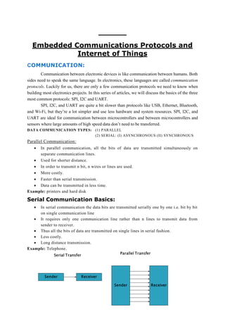
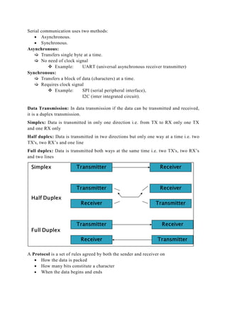
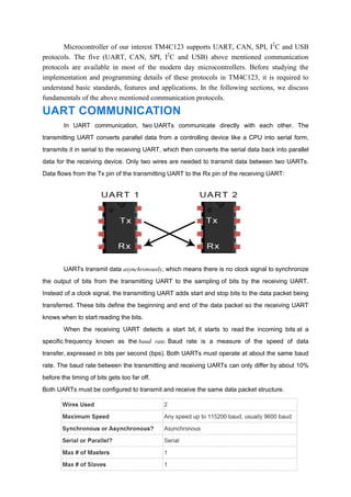
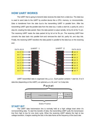
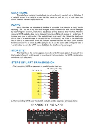
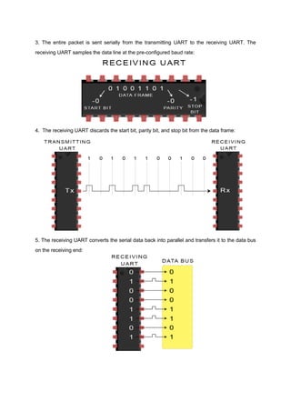
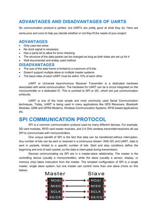
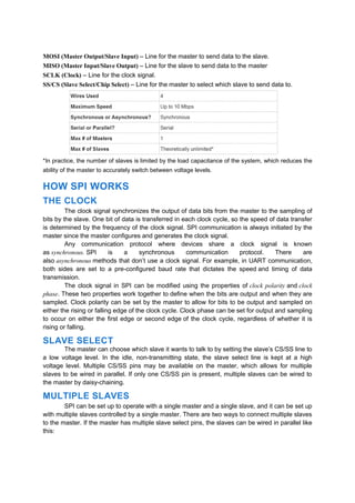
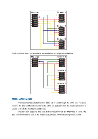
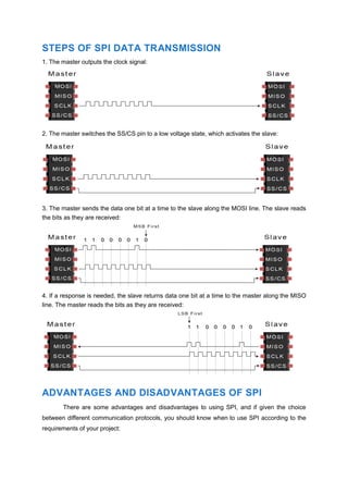
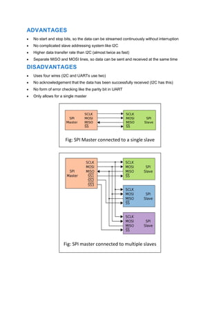
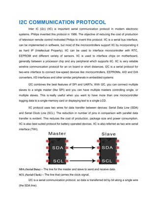
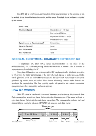
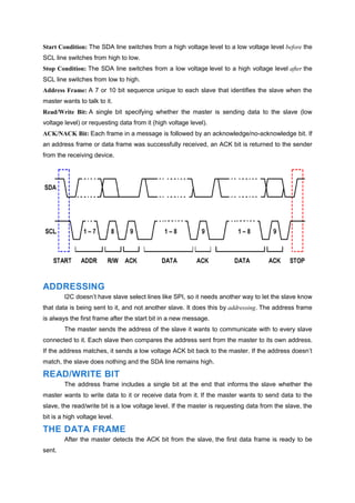
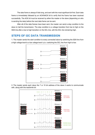
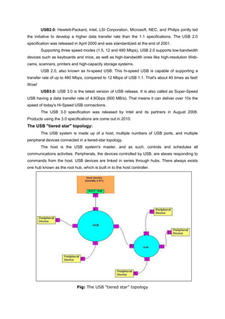
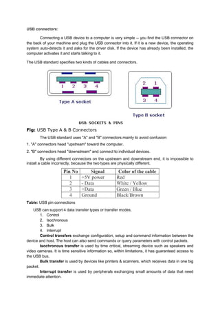
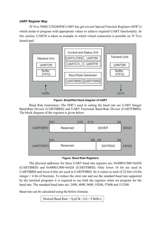
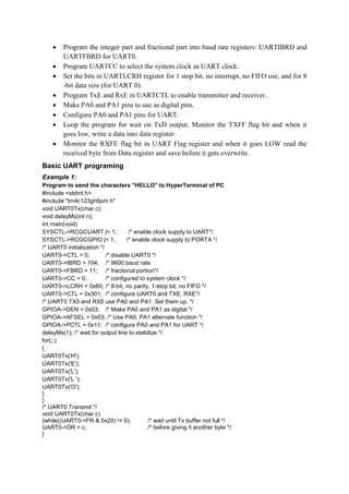
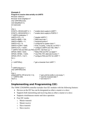
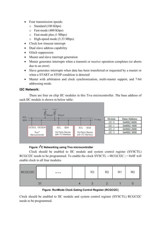
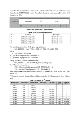
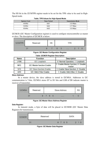
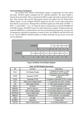
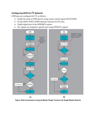
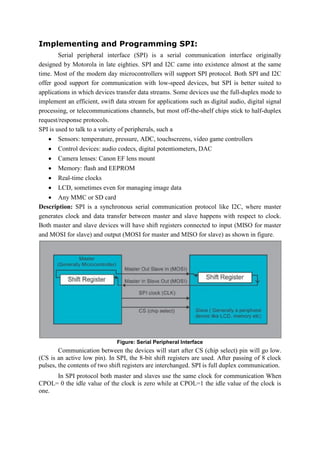
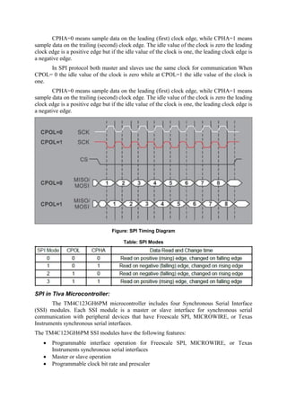
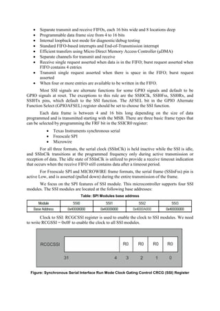
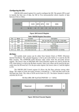
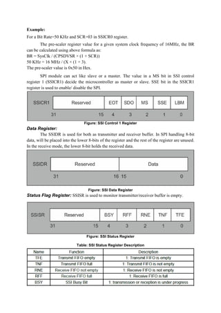
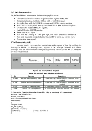
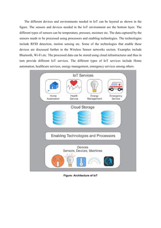
SlideShare a Scribd company logo
1 of 65
Download to read offline
Embedded Communications Protocols and
Internet of Things
COMMUNICATION:
Communication between electronic devices is like communication between humans. Both
sides need to speak the same language. In electronics, these languages are called communication
protocols. Luckily for us, there are only a few communication protocols we need to know when
building most electronics projects. In this series of articles, we will discuss the basics of the three
most common protocols: SPI, I2C and UART.
SPI, I2C, and UART are quite a bit slower than protocols like USB, Ethernet, Bluetooth,
and Wi-Fi, but they’re a lot simpler and use less hardware and system resources. SPI, I2C, and
UART are ideal for communication between microcontrollers and between microcontrollers and
sensors where large amounts of high speed data don’t need to be transferred.
DATA COMMUNICATION TYPES: (1) PARALLEL
(2) SERIAL: (I) ASYNCHRONOUS (II) SYNCHRONOUS
Parallel Communication:
 In parallel communication, all the bits of data are transmitted simultaneously on
separate communication lines.
 Used for shorter distance.
 In order to transmit n bit, n wires or lines are used.
 More costly.
 Faster than serial transmission.
 Data can be transmitted in less time.
Example: printers and hard disk
Serial Communication Basics:
 In serial communication the data bits are transmitted serially one by one i.e. bit by bit
on single communication line
 It requires only one communication line rather than n lines to transmit data from
sender to receiver.
 Thus all the bits of data are transmitted on single lines in serial fashion.
 Less costly.
 Long distance transmission.
Example: Telephone.
Serial communication uses two methods:
 Asynchronous.
 Synchronous.
Asynchronous:
 Transfers single byte at a time.
 No need of clock signal
 Example: UART (universal asynchronous receiver transmitter)
Synchronous:
 Transfers a block of data (characters) at a time.
 Requires clock signal
 Example: SPI (serial peripheral interface),
I2C (inter integrated circuit).
Data Transmission: In data transmission if the data can be transmitted and received,
it is a duplex transmission.
Simplex: Data is transmitted in only one direction i.e. from TX to RX only one TX
and one RX only
Half duplex: Data is transmitted in two directions but only one way at a time i.e. two
TX's, two RX’s and one line
Full duplex: Data is transmitted both ways at the same time i.e. two TX's, two RX’s
and two lines
A Protocol is a set of rules agreed by both the sender and receiver on
 How the data is packed
 How many bits constitute a character
 When the data begins and ends
Table: Various Serial Communication Protocols
Serial
Protocol
Synchronous
/Asynchronous
Type Duplex
Data transfer
rate (kbps)
UART Asynchronous peer-to-peer Full-duplex 20
I2C Synchronous multi-master Half-duplex 3400
SPI Synchronous multi-master Full-duplex >1,000
MICROWIRE Synchronous master/slave Full-duplex > 625
1-WIRE Asynchronous master/slave Half-duplex 16
Baud Rate Concepts:
Data transfer rate in serial communication is measured in terms of bits per second
(bps). This is also called as Baud Rate. Baud Rate and bps can be used inter changeably with
respect to UART.
Ex: The total number of bits gets transferred during 10 pages of text, each with 100 ×
25 characters with 8 bits per character and 1 start & stop bit is:
For each character a total number of bits are 10. The total number of bits is:
100 × 25 × 10 = 25,000 bits per page. For 10 pages of data it is required to transmit 2, 50,000
bits. Generally baud rates of SCI are 1200, 2400, 4800, 9600, 19,200 etc. To transfer 2,
50,000 bits at a baud rate of 9600, we need: 250000/9600 = 26.04 seconds (27 seconds).
Synchronous/Asynchronous Interfaces (like UART, SPI,
I2C, and USB):
Serial communication protocols can be categorized as Synchronous and
Asynchronous protocols. In synchronous communication, data is transmission and receiving
is a continuous stream at a constant rate. Synchronous communication requires the clock of
transmitting device and receiving device synchronized. In most of the systems, like ADC,
audio codes, potentiometers, transmission and reception of data occurs with same frequency.
Examples of synchronous communication are: I2C, SPI etc. In the case of asynchronous
communication, the transmission of data requires no clock signal and data transfer occurs
intermittently rather than steady stream. Handshake signals between the transmitter and
receiver are important in asynchronous communications. Examples of asynchronous
communication are Universal Asynchronous Receiver Transmitter (UART), CAN etc.
Synchronous and asynchronous communication protocols are well-defined standards
and can be implemented in either hardware or software. In the early days of embedded
systems, Software implementation of I2
C and SPI was common as well as a tedious work and
used to take long programs. Gradually, most the microcontrollers started incorporating the
standard communication protocols as hardware cores. This development in early 90‟s made
job of the embedded software development easy for communication protocols.
Microcontroller of our interest TM4C123 supports UART, CAN, SPI, I2
C and USB
protocols. The five (UART, CAN, SPI, I2
C and USB) above mentioned communication
protocols are available in most of the modern day microcontrollers. Before studying the
implementation and programming details of these protocols in TM4C123, it is required to
understand basic standards, features and applications. In the following sections, we discuss
fundamentals of the above mentioned communication protocols.
UART COMMUNICATION
In UART communication, two UARTs communicate directly with each other. The
transmitting UART converts parallel data from a controlling device like a CPU into serial form,
transmits it in serial to the receiving UART, which then converts the serial data back into parallel
data for the receiving device. Only two wires are needed to transmit data between two UARTs.
Data flows from the Tx pin of the transmitting UART to the Rx pin of the receiving UART:
UARTs transmit data asynchronously, which means there is no clock signal to synchronize
the output of bits from the transmitting UART to the sampling of bits by the receiving UART.
Instead of a clock signal, the transmitting UART adds start and stop bits to the data packet being
transferred. These bits define the beginning and end of the data packet so the receiving UART
knows when to start reading the bits.
When the receiving UART detects a start bit, it starts to read the incoming bits at a
specific frequency known as the baud rate. Baud rate is a measure of the speed of data
transfer, expressed in bits per second (bps). Both UARTs must operate at about the same baud
rate. The baud rate between the transmitting and receiving UARTs can only differ by about 10%
before the timing of bits gets too far off.
Both UARTs must be configured to transmit and receive the same data packet structure.
HOW UART WORKS
The UART that is going to transmit data receives the data from a data bus. The data bus
is used to send data to the UART by another device like a CPU, memory, or microcontroller.
Data is transferred from the data bus to the transmitting UART in parallel form. After the
transmitting UART gets the parallel data from the data bus, it adds a start bit, a parity bit, and a
stop bit, creating the data packet. Next, the data packet is output serially, bit by bit at the Tx pin.
The receiving UART reads the data packet bit by bit at its Rx pin. The receiving UART then
converts the data back into parallel form and removes the start bit, parity bit, and stop bits.
Finally, the receiving UART transfers the data packet in parallel to the data bus on the receiving
end:
UART transmitted data is organized into packets. Each packet contains 1 start bit, 5 to 9
data bits (depending on the UART), an optional parity bit, and 1 or 2 stop bits:
START BIT
The UART data transmission line is normally held at a high voltage level when it’s
not transmitting data. To start the transfer of data, the transmitting UART pulls the transmission
line from high to low for one clock cycle. When the receiving UART detects the high to low
voltage transition, it begins reading the bits in the data frame at the frequency of the baud rate.
DATA FRAME
The data frame contains the actual data being transferred. It can be 5 bits to 9 bits long if
a parity bit is used. If no parity bit is used, the data frame can be 8 bits long. In most cases, the
data is sent with the least significant bit first.
PARITY
Parity describes the evenness or oddness of a number. The parity bit is a way for the
receiving UART to tell if any data has changed during transmission. Bits can be changed
by electromagnetic radiation, mismatched baud rates, or long distance data transfers. After the
receiving UART reads the data frame, it counts the number of bits with a value of 1 and checks if
the total is an even or odd number. If the parity bit is a 0 (even parity), the 1 bits in the data frame
should total to an even number. If the parity bit is a 1 (odd parity), the 1 bits in the data frame
should total to an odd number. When the parity bit matches the data, the UART knows that the
transmission was free of errors. But if the parity bit is a 0, and the total is odd; or the parity bit is a
1, and the total is even, the UART knows that bits in the data frame have changed.
STOP BITS
The Stop Bit, as the name suggests, marks the end of the data packet. It is usually two
bits long but often only on bit is used. In order to end the transmission, the UART maintains the
data line at high voltage (1).
STEPS OF UART TRANSMISSION
1. The transmitting UART receives data in parallel from the data bus:
2. The transmitting UART adds the start bit, parity bit, and the stop bit(s) to the data frame:
3. The entire packet is sent serially from the transmitting UART to the receiving UART. The
receiving UART samples the data line at the pre-configured baud rate:
4. The receiving UART discards the start bit, parity bit, and stop bit from the data frame:
5. The receiving UART converts the serial data back into parallel and transfers it to the data bus
on the receiving end:
ADVANTAGES AND DISADVANTAGES OF UARTS
No communication protocol is perfect, but UARTs are pretty good at what they do. Here are
some pros and cons to help you decide whether or not they fit the needs of your project:
ADVANTAGES
 Only uses two wires
 No clock signal is necessary
 Has a parity bit to allow for error checking
 The structure of the data packet can be changed as long as both sides are set up for it
 Well documented and widely used method
DISADVANTAGES
 The size of the data frame is limited to a maximum of 9 bits
 Doesn’t support multiple slave or multiple master systems
 The baud rates of each UART must be within 10% of each other
UART or Universal Asynchronous Receiver Transmitter is a dedicated hardware
associated with serial communication. The hardware for UART can be a circuit integrated on the
microcontroller or a dedicated IC. This is contrast to SPI or I2C, which are just communication
protocols.
UART is one of the most simple and most commonly used Serial Communication
techniques. Today, UART is being used in many applications like GPS Receivers, Bluetooth
Modules, GSM and GPRS Modems, Wireless Communication Systems, RFID based applications
etc.
SPI COMMUNICATION PROTOCOL
SPI is a common communication protocol used by many different devices. For example,
SD card modules, RFID card reader modules, and 2.4 GHz wireless transmitter/receivers all use
SPI to communicate with microcontrollers.
One unique benefit of SPI is the fact that data can be transferred without interruption.
Any number of bits can be sent or received in a continuous stream. With I2C and UART, data is
sent in packets, limited to a specific number of bits. Start and stop conditions define the
beginning and end of each packet, so the data is interrupted during transmission.
Devices communicating via SPI are in a master-slave relationship. The master is the
controlling device (usually a microcontroller), while the slave (usually a sensor, display, or
memory chip) takes instruction from the master. The simplest configuration of SPI is a single
master, single slave system, but one master can control more than one slave (more on this
below).
MOSI (Master Output/Slave Input) – Line for the master to send data to the slave.
MISO (Master Input/Slave Output) – Line for the slave to send data to the master
SCLK (Clock) – Line for the clock signal.
SS/CS (Slave Select/Chip Select) – Line for the master to select which slave to send data to.
*In practice, the number of slaves is limited by the load capacitance of the system, which reduces the
ability of the master to accurately switch between voltage levels.
HOW SPI WORKS
THE CLOCK
The clock signal synchronizes the output of data bits from the master to the sampling of
bits by the slave. One bit of data is transferred in each clock cycle, so the speed of data transfer
is determined by the frequency of the clock signal. SPI communication is always initiated by the
master since the master configures and generates the clock signal.
Any communication protocol where devices share a clock signal is known
as synchronous. SPI is a synchronous communication protocol. There are
also asynchronous methods that don’t use a clock signal. For example, in UART communication,
both sides are set to a pre-configured baud rate that dictates the speed and timing of data
transmission.
The clock signal in SPI can be modified using the properties of clock polarity and clock
phase. These two properties work together to define when the bits are output and when they are
sampled. Clock polarity can be set by the master to allow for bits to be output and sampled on
either the rising or falling edge of the clock cycle. Clock phase can be set for output and sampling
to occur on either the first edge or second edge of the clock cycle, regardless of whether it is
rising or falling.
SLAVE SELECT
The master can choose which slave it wants to talk to by setting the slave’s CS/SS line to
a low voltage level. In the idle, non-transmitting state, the slave select line is kept at a high
voltage level. Multiple CS/SS pins may be available on the master, which allows for multiple
slaves to be wired in parallel. If only one CS/SS pin is present, multiple slaves can be wired to
the master by daisy-chaining.
MULTIPLE SLAVES
SPI can be set up to operate with a single master and a single slave, and it can be set up
with multiple slaves controlled by a single master. There are two ways to connect multiple slaves
to the master. If the master has multiple slave select pins, the slaves can be wired in parallel like
this:
If only one slave select pin is available, the slaves can be daisy-chained like this:
MOSI AND MISO
The master sends data to the slave bit by bit, in serial through the MOSI line. The slave
receives the data sent from the master at the MOSI pin. Data sent from the master to the slave is
usually sent with the most significant bit first.
The slave can also send data back to the master through the MISO line in serial. The
data sent from the slave back to the master is usually sent with the least significant bit first.
STEPS OF SPI DATA TRANSMISSION
1. The master outputs the clock signal:
2. The master switches the SS/CS pin to a low voltage state, which activates the slave:
3. The master sends the data one bit at a time to the slave along the MOSI line. The slave reads
the bits as they are received:
4. If a response is needed, the slave returns data one bit at a time to the master along the MISO
line. The master reads the bits as they are received:
ADVANTAGES AND DISADVANTAGES OF SPI
There are some advantages and disadvantages to using SPI, and if given the choice
between different communication protocols, you should know when to use SPI according to the
requirements of your project:
ADVANTAGES
 No start and stop bits, so the data can be streamed continuously without interruption
 No complicated slave addressing system like I2C
 Higher data transfer rate than I2C (almost twice as fast)
 Separate MISO and MOSI lines, so data can be sent and received at the same time
DISADVANTAGES
 Uses four wires (I2C and UARTs use two)
 No acknowledgement that the data has been successfully received (I2C has this)
 No form of error checking like the parity bit in UART
 Only allows for a single master
Fig: SPI Master connected to a single slave
Fig: SPI master connected to multiple slaves
I2C COMMUNICATION PROTOCOL
Inter IC (i2c) (IIC) is important serial communication protocol in modern electronic
systems. Philips invented this protocol in 1986. The objective of reducing the cost of production
of television remote control motivated Philips to invent this protocol. IIC is a serial bus interface,
can be implemented in software, but most of the microcontrollers support IIC by incorporating it
as hard IP (Intellectual Property). IIC can be used to interface microcontroller with RTC,
EEPROM and different variety of sensors. IIC is used to interface chips on motherboard,
generally between a processor chip and any peripheral which supports IIC. IIC is very reliable
wireline communication protocol for an on board or short distances. I2C is a serial protocol for
two-wire interface to connect low-speed devices like microcontrollers, EEPROMs, A/D and D/A
converters, I/O interfaces and other similar peripherals in embedded systems
I2C combines the best features of SPI and UARTs. With I2C, you can connect multiple
slaves to a single master (like SPI) and you can have multiple masters controlling single, or
multiple slaves. This is really useful when you want to have more than one microcontroller
logging data to a single memory card or displaying text to a single LCD.
IIC protocol uses two wires for data transfer between devices: Serial Data Line (SDA)
and Serial Clock Line (SCL). The reduction in number of pins in comparison with parallel data
transfer is evident. This reduces the cost of production, package size and power consumption.
IIC is also best suited protocol for battery operated devices. IIC is also referred as two wire serial
interface (TWI).
SDA (Serial Data) – The line for the master and slave to send and receive data.
SCL (Serial Clock) – The line that carries the clock signal.
I2C is a serial communication protocol, so data is transferred bit by bit along a single wire
(the SDA line).
Like SPI, I2C is synchronous, so the output of bits is synchronized to the sampling of bits
by a clock signal shared between the master and the slave. The clock signal is always controlled
by the master.
GENERAL ELECTRICAL CHARACTERISTICS OF I2C
To implement I2C (For TIVA series microcontrollers or for most of the
microcontrollers) a 4.7kilo ohm pull-up resistor for each line is needed. This is required to
implement wired-AND logic in IIC.
More than 100 devices can be connected to I2C bus theoretically. It is better to restrict
to 15 devices for better performance of the network. Each device is called as node. Nodes
which generates clock are called Master nodes and devices which work based on the clock
generated by master node are called Slave nodes. Generally, master nodes initiate and
terminate the transmission. The four possible modes of operation are: master transmitter,
master receiver, slave transmitter and slave receiver.
HOW I2C WORKS
With I2C, data is transferred in messages. Messages are broken up into frames of data.
Each message has an address frame that contains the binary address of the slave, and one or
more data frames that contain the data being transmitted. The message also includes start and
stop conditions, read/write bits, and ACK/NACK bits between each data frame:
Start Condition: The SDA line switches from a high voltage level to a low voltage level before the
SCL line switches from high to low.
Stop Condition: The SDA line switches from a low voltage level to a high voltage level after the
SCL line switches from low to high.
Address Frame: A 7 or 10 bit sequence unique to each slave that identifies the slave when the
master wants to talk to it.
Read/Write Bit: A single bit specifying whether the master is sending data to the slave (low
voltage level) or requesting data from it (high voltage level).
ACK/NACK Bit: Each frame in a message is followed by an acknowledge/no-acknowledge bit. If
an address frame or data frame was successfully received, an ACK bit is returned to the sender
from the receiving device.
ADDRESSING
I2C doesn’t have slave select lines like SPI, so it needs another way to let the slave know
that data is being sent to it, and not another slave. It does this by addressing. The address frame
is always the first frame after the start bit in a new message.
The master sends the address of the slave it wants to communicate with to every slave
connected to it. Each slave then compares the address sent from the master to its own address.
If the address matches, it sends a low voltage ACK bit back to the master. If the address doesn’t
match, the slave does nothing and the SDA line remains high.
READ/WRITE BIT
The address frame includes a single bit at the end that informs the slave whether the
master wants to write data to it or receive data from it. If the master wants to send data to the
slave, the read/write bit is a low voltage level. If the master is requesting data from the slave, the
bit is a high voltage level.
THE DATA FRAME
After the master detects the ACK bit from the slave, the first data frame is ready to be
sent.
The data frame is always 8 bits long, and sent with the most significant bit first. Each data
frame is immediately followed by an ACK/NACK bit to verify that the frame has been received
successfully. The ACK bit must be received by either the master or the slave (depending on who
is sending the data) before the next data frame can be sent.
After all of the data frames have been sent, the master can send a stop condition to the
slave to halt the transmission. The stop condition is a voltage transition from low to high on the
SDA line after a low to high transition on the SCL line, with the SCL line remaining high.
STEPS OF I2C DATA TRANSMISSION
1. The master sends the start condition to every connected slave by switching the SDA line from
a high voltage level to a low voltage level before switching the SCL line from high to low:
2. The master sends each slave the 7 or 10 bit address of the slave it wants to communicate
with, along with the read/write bit:
3. Each slave compares the address sent from the master to its own address. If the address
matches, the slave returns an ACK bit by pulling the SDA line low for one bit. If the address from
the master does not match the slave’s own address, the slave leaves the SDA line high.
4. The master sends or receives the data frame:
5. After each data frame has been transferred, the receiving device returns another ACK bit to
the sender to acknowledge successful receipt of the frame:
6. To stop the data transmission, the master sends a stop condition to the slave by
switching SCL high before switching SDA high:
SINGLE MASTER WITH MULTIPLE SLAVES
Because I2C uses addressing, multiple slaves can be controlled from a single master.
With a 7 bit address, 128 (27
) unique address are available. Using 10 bit addresses is
uncommon, but provides 1,024 (210
) unique addresses. To connect multiple slaves to a single
master, wire them like this, with 4.7K/10K Ohm pull-up resistors connecting the SDA and SCL
lines to Vcc:
MULTIPLE MASTERS WITH MULTIPLE SLAVES
Multiple masters can be connected to a single slave or multiple slaves. The problem with
multiple masters in the same system comes when two masters try to send or receive data at the
same time over the SDA line. To solve this problem, each master needs to detect if the SDA line
is low or high before transmitting a message. If the SDA line is low, this means that another
master has control of the bus, and the master should wait to send the message. If the SDA line is
high, then it’s safe to transmit the message. To connect multiple masters to multiple slaves, use
the following diagram, with 4.7K Ohm pull-up resistors connecting the SDA and SCL lines to Vcc:
ADVANTAGES AND DISADVANTAGES OF I2C
There is a lot to I2C that might make it sound complicated compared to other protocols,
but there are some good reasons why you may or may not want to use I2C to connect to a
particular device:
ADVANTAGES
 Only uses two wires
 Supports multiple masters and multiple slaves
 ACK/NACK bit gives confirmation that each frame is transferred successfully
 Hardware is less complicated than with UARTs
 Well known and widely used protocol
DISADVANTAGES
 Slower data transfer rate than SPI
 The size of the data frame is limited to 8 bits
 More complicated hardware needed to implement than SPI
UNIVERSAL SERIAL BUS (USB)
Universal Serial Bus (USB) is a set of interface specifications for high speed wired
communication between electronics systems peripherals and devices with or without
PC/computer. The USB was originally developed in 1995 by many of the industry leading
companies like Intel, Compaq, Microsoft, Digital, IBM, and Northern Telecom.
The major goal of USB was to define an external expansion bus to add peripherals to a
PC in easy and simple manner.
USB offers users simple connectivity. It eliminates the mix of different connectors for
different devices like printers, keyboards, mice, and other peripherals. That means USB-bus
allows many peripherals to be connected using a single standardized interface socket. It supports
all kinds of data, from slow mouse inputs to digitized audio and compressed video.
USB also allows hot swapping. The "hot-swapping" means that the devices can be
plugged and unplugged without rebooting the computer or turning off the device. That means,
when plugged in, everything configures automatically. Once the user is finished, they can simply
unplug the cable out; the host will detect its absence and automatically unload the driver. This
makes the USB a plug-and-play interface between a computer and add-on devices.
USB is now the most used interface to connect devices like mouse, keyboards, PDAs,
game-pads and joysticks, scanners, digital cameras, printers, personal media players, and flash
drives to personal computers.
USB sends data in serial mode i.e. the parallel data is serialized before sends and de-
serialized after receiving.
The benefits of USB are low cost, expandability, auto-configuration, hot-plugging and
outstanding performance. It also provides power to the bus, enabling many peripherals to
operate without the added need for an AC power adapter.
Various versions USB:
USB1.0: USB 1.0 is the original release of USB having the capability of transferring
12Mbps, supporting up to 127 devices. This USB 1.0 specification model was introduced in
January 1996.
USB1.1: USB 1.1 came out in September 1998. USB 1.1 is also known as full-speed
USB. This version is similar to the original release of USB; however, there are minor
modifications for the hardware and the specifications. USB version 1.1 supported two speeds, a
full speed mode of 12Mbits/s and a low speed mode of 1.5Mbits/s.
USB2.0: Hewlett-Packard, Intel, LSI Corporation, Microsoft, NEC, and Philips jointly led
the initiative to develop a higher data transfer rate than the 1.1 specifications. The USB 2.0
specification was released in April 2000 and was standardized at the end of 2001.
Supporting three speed modes (1.5, 12 and 480 Mbps), USB 2.0 supports low-bandwidth
devices such as keyboards and mice, as well as high-bandwidth ones like high-resolution Web-
cams, scanners, printers and high-capacity storage systems.
USB 2.0, also known as hi-speed USB. This hi-speed USB is capable of supporting a
transfer rate of up to 480 Mbps, compared to 12 Mbps of USB 1.1. That's about 40 times as fast!
Wow!
USB3.0: USB 3.0 is the latest version of USB release. It is also called as Super-Speed
USB having a data transfer rate of 4.8Gbps (600 MB/s). That means it can deliver over 10x the
speed of today's Hi-Speed USB connections.
The USB 3.0 specification was released by Intel and its partners in August 2008.
Products using the 3.0 specifications are come out in 2010.
The USB "tiered star" topology:
The USB system is made up of a host, multiple numbers of USB ports, and multiple
peripheral devices connected in a tiered-star topology.
The host is the USB system's master, and as such, controls and schedules all
communications activities. Peripherals, the devices controlled by USB, are slaves responding to
commands from the host. USB devices are linked in series through hubs. There always exists
one hub known as the root hub, which is built in to the host controller.
Fig: The USB "tiered star" topology
USB connectors:
Connecting a USB device to a computer is very simple -- you find the USB connector on
the back of your machine and plug the USB connector into it. If it is a new device, the operating
system auto-detects it and asks for the driver disk. If the device has already been installed, the
computer activates it and starts talking to it.
The USB standard specifies two kinds of cables and connectors.
Fig: USB Type A & B Connectors
The USB standard uses "A" and "B" connectors mainly to avoid confusion:
1. "A" connectors head "upstream" toward the computer.
2. "B" connectors head "downstream" and connect to individual devices.
By using different connectors on the upstream and downstream end, it is impossible to
install a cable incorrectly, because the two types are physically different.
Pin No Signal Color of the cable
1 +5V power Red
2 - Data White / Yellow
3 +Data Green / Blue
4 Ground Black/Brown
Table: USB pin connections
USB can support 4 data transfer types or transfer modes.
1. Control
2. Isochronous
3. Bulk
4. Interrupt
Control transfers exchange configuration, setup and command information between the
device and host. The host can also send commands or query parameters with control packets.
Isochronous transfer is used by time critical, streaming device such as speakers and
video cameras. It is time sensitive information so, within limitations, it has guaranteed access to
the USB bus.
Bulk transfer is used by devices like printers & scanners, which receives data in one big
packet.
Interrupt transfer is used by peripherals exchanging small amounts of data that need
immediate attention.
All USB data is sent serially. USB data transfer is essentially in the form of packets of
data, sent back and forth between the host and peripheral devices. Initially all packets are sent
from the host, via the root hub and possibly more hubs, to devices.
Each USB data transfer consists of a…
1. Token packet (Header defining what it expects to follow)
2. Optional Data Packet (Containing the payload)
3. Status Packet (Used to acknowledge transactions and to provide a means of error
correction).
Implementing and Programming UART:
TM4C123GH6PM microcontroller has got eight UART ports. They are named as
UART0-UART7. In the TI Launchpad, the UART0 port is connected to the ICDI (In-Circuit
Debug Interface). ICDI is further connected to USB port. Users can use UART0 for flash
programming, debugging using JTAG. The UART features of TI Tiva TM4C123GH6PM
microcontroller is: -
 UART‟s have programmable baud-rate generator allowing speeds up to 5 Mbps for
regular speed and 10 Mbps for high speed.
 Separate 16x8 transmit (TX) and receive (RX) FIFOs to reduce CPU interrupt service
loading with programmable FIFO length
 Standard asynchronous communication bits for start, stop, and parity, Line-break
generation and detection
 Fully programmable serial interface characteristics
o 5, 6, 7, or 8 data bits
o Even, odd, stick, or no-parity bit generation/detection
o 1 or 2 stop bit generation
 IrDA serial-IR (SIR) encoder/decoder providing
o Programmable use of IrDA Serial Infrared (SIR) or UART input/output
o Support of IrDA SIR encoder/decoder functions for data rates up to 115.2 Kbps
half duplex
o Support of normal 3/16 and low-power (1.41-2.23 μs) bit durations
o Programmable internal clock generator enabling division of reference clock by 1
to 256 for low-power mode bit duration
 Support for communication with ISO 7816 smart cards
 Modem flow control (on UART1)
 EIA-485 9-bit support
 Standard FIFO-level and End-of-Transmission interrupts
 Efficient transfers using Micro Direct Memory Access Controller (μDMA)
o Separate channels for transmit and receive
o Receive single request asserted when data is in the FIFO; burst request asserted at
programmed FIFO level Transmit single request asserted when there is space in
the FIFO; burst request asserted at programmed FIFO level.
UART Register Map
TI Tiva TM4C123GH6PM UART has got several Special Function Registers (SFR‟s)
which needs to program with appropriate values to achieve required UART functionality. In
this section, UART0 is taken as example in which virtual connection is possible on TI Tiva
launch pad.
Figure: Simplified block diagram of UART
Baud Rate Generators: The SFR‟s used in setting the baud rate are UART Integer
Baud-Rate Divisor (UARTIBRD) and UART Fractional Baud-Rate Divisor (UARTFBRD).
The block diagram of the registers is given below:
Figure: Baud Rate Registers
The physical addresses for these UART baud rate registers are: 0x4000:C000+0x024
(UARTIBRD) and 0x4000:C000+0x028 (UARTFBRD). Only lower 16 bit are used in
UARTIBRD and lower 6-bits are used in UARTFBRD. So it comes to total of 22 bits (16-bit
integer + 6 bit of fraction). To reduce the error rate and use the standard baud rate supported
by the terminal programs it is required to use both the registers when we program for the
baud rate. The standard baud rates are: 2400, 4800, 9600, 19200, 57600 and 115200.
Baud rate can be calculated using the below formula:
Desired Baud Rate = SysClk / (16 × ClkDiv)
Where the SysClk is the working system clock connected to the UART and ClkDiv is
the value programmed into baud rate registers.
The baud-rate divisor (BRD) has the following relationship to the system clock,
where BRDI is the integer part of the BRD and BRDF is the fractional part, separated by a
decimal place.
UARTSysClk is the system clock connected to the UART, and ClkDiv is 16 (if HSE
in UARTCTL is clear) or 8 (if HSE is set).
Alternatively, the UART may be clocked from the internal precision oscillator
(PIOSC), independent of the system clock selection. This will allow the UART clock to be
programmed independently of the system clock PLL settings.
TI Tiva Launchpad system clock is 16 MHz so desired Baud Rate can be calculated as:
The ClkDiv value includes both integer and fractional values loaded into UARTIBRD
and UARTFBRD registers. The integer part is easy to calculate and fraction part requires
manipulations based on trial and error.
Example:
System clock of TI Tiva Launchpad is16 MHz 16MHz is divided by 16 and it is fed
into UART. So UART operates at 1MHz frequency. So ClkDiv = 1MHz.
To generate a baud rate of 4800: 1MHz/4800 = 208.33
(a) 1MHz/4800 = 208.33, UARTIBRD=208 & UARTFBRD = (0.33×64) + 0.5 = 21.83 =21
(b) 1MHz/9600 = 104.166666, UARTIBRD = 104 & UARTFBRD = (0.16666×64) +0.5=11
(c) 1MHz/57600 = 17.361, UARTIBRD = 17 and UARTFBRD = (0.361 × 64) + 0.5 =23
(d) 1MHz/115200 = 8.680, UARTIBRD = 8 and UARTFBRD = (0.680 × 64) +0.5=44
Serial IR (SIR):
UART includes an IrDA (Infrared) serial IR encoder-decoder block. SIR block
converts the data between UART and half-duplex serial SIR interface. The SIR block
provides a digitally encoded output and decoded input to UART. SIR block uses UnTx and
UnRx pins for SIR interface. These pins are connected to IrDA SIR physical layer link. SIR
block supports half-duplex communication. The IrDA SIR physical layer specifies a
minimum 10-ms delay between transmission and reception. The SIR block has two modes of
operation normal mode and low power mode.
ISO 7816 Support: UART support ISO 7816 smartcard communication. The UnTx signal is
used as a bit clock and the UnRx signal is used as the half-duplex communication line
connected to the smartcard. Any GPIO signal can be used to generate the reset signal to the
smartcard.
BRD = BRDI + BRDF = UARTSysClk / (ClkDiv * Baud Rate)
Baud Rate = 16MHz / (16 × ClkDiv) = 1MHz / ClkDiv
UART Control Register (UARTCTL):
This is a 32-bit register. The most important bits are RXE, TXE, HSE, and UARTEN.
Figure: UART Control Register (UARTCTL)
 RXE (Receive enable): This bit should be enabled to receive data.
 TXE (Transmit Enable): This bit should be enabled to transmit data.
 HSE (High Speed enable): This bit is used to set the baud rate. By default the system
clock is divided by 16 before it is fed to the UART. The user can program HSE =1, to
make system clock divide by 8.
 UARTEN (UART enable): This bit allows user to enable or disable the UART. During
the initialization of the UART registers, this is disabled. To disable UART under any
circumstances, this bit is used.
 SIREN (SIR Enable): IrDA SIR Block is enabled. UART will transmit and receive data
using SIR protocol.
 SIRLP (SIR Low Power Mode): This bit selects the IrDA encoding mode: Normal
mode or low power mode.
 SMART (ISO 7816 Smart Card support): The UART operates in Smart Card mode
when SMART = 1. UART does not support automatic retransmission on parity errors.
If a parity error is detected on transmission, all further transmit operations are aborted
and software must handle retransmission of the affected byte or message.
 LBE (Loop Back Enable): The UnTx path is fed through the UnRx path when LBE =1.
 RTSEN (Enable Request to send): RTS hardware flow control is enabled. Data is only
requested when receive FIFO has available entries.
 RTS (Request to send): When RTSEN is clear, the status of this bit is reflected on the
U1RTS signal. If RTSEN is set, this bit is ignored on a write and should be ignored on
read.
UART Line Control Register (UARTLCTH)
This register is used to set the length of data. The bits per character in a frame and
number of stop bits are also decided.
 STP2 (Stop bit2): The stop bits can be 1 or 2. The default is 1 stop bit at the end of
each frame. If the receiving device is slow, we can use 2 stop bits by making the
STP2=1.
 FEN (FIFO Enable): UART has an internal 16-byte FIFO (first in first out) buffer to
store data for transmission to keep the CPU getting interrupted for the reception and
transmission of every byte. Enabling FEN bit, we can write up to16 bytes of data
block into its transmission FIFO buffer and let transfer happen one byte at a time.
There is also a separate 16 byte FIFO for the receiver to buffer the incoming data.
Upon Reset, the default for FIFO buffer size is 1 byte.
 WLEN (Word Length): The number of bits per character data in each frame can be 5,
6, 7, or 8. we use 8 bits for each character data frame. Default world length mode is 5.
 BRK (Send Break): A Low level is continually output on the UnTx signal, after
completing transmission of the current character. For the proper execution of the
break command, software must set this bit for at least two frames (character periods).
 PEN (Parity Enable): Parity is enabled and parity bit is added to the data frame by
making PEN = 1. Parity checking is also enabled.
 EPS (Even Parity Select): Odd parity is performed, which checks for an odd number
of 1s when EPS = 0. Even parity generation and checking is performed during
transmission and reception, which checks for an even number of 1s in data and parity
bits when EPS = 1.
UART Data Register (UARTDR):
Figure: UART Date Register (UARTDR)
Data should be placed in data register before transmission. Only lower 8 bits are used.
In a similar way, the received byte should be read and saved in memory before it gets
overwrite by next byte. During reception, we use other four bits (8, 9, 10 and 11) to detect
error, parity etc. Another set of registers are used to check the source of error.
(UARTRSR/UARTRCR)
 OE: Overrun error (OE = 0: No data is lost).
 BE: Break error
 PE: Parity error
 FE: Framing error.
UART Flag Register (UARTFR):
The UART Flag Register holds one byte of data when FIFO buffer is disabled.
Figure: UART Flag Register (UARTFR)
 TXFE (TX FIFO Empty): Transmitter loads one byte for transmission from the FIFO
buffer.
 When FIFO becomes empty, the TXFE is raised. The transmitter then frames the byte
and sends it out via TxD pin bit by bit serially.
 RXFF (RX FIFO Full): When a byte of data is received, byte is placed in Data
register and RXFF (RX FIFO full) flag bit is raised after receiving the complete byte.
 TXFF (TX FIFOI Full): When the transmitter is not busy, it loads one byte from the
FIFO buffer and the FIFO is not full anymore and the TXFF is lowered. We can
monitor TXFF flag and upon going LOW we can write another byte to the Data
register.
UART Transmission
Step to perform UART Transmission:
 Program the RCGCUART register to get clock on UART0.
 Program the RCGCGPIO register to get the clock for PORTA.
 Program UARTCTL to disable UART0.
 Program the integer part and fractional part into baud rate registers: UARTIBRD and
UARTFBRD for UART0.
 Program UARTCC to select the system clock as UART clock.
 Set the bits in UARTLCRH register for 1 stop bit, no interrupt, no FIFO use, and for 8-
bit date size (for UART 0).
 Program TxE and RxE in UARTCTL to enable transmitter and receiver.
 Make PA0 and PA1 pins to use as digital pins.
 Configure PA0 and PA1 pins for UART.
 Loop the program for wait on TxD output. Monitor the TXFF flag bit and when it goes
low, write a data into data register.
UART Reception
Step by Step Execution of UART Reception:
 Program the RCGCUART register to get clock on UART0.
 Program the RCGCGPIO register to get the clock for PORTA.
 Program UARTCTL to disable UART0.
 Program the integer part and fractional part into baud rate registers: UARTIBRD and
UARTFBRD for UART0.
 Program UARTCC to select the system clock as UART clock.
 Set the bits in UARTLCRH register for 1 stop bit, no interrupt, no FIFO use, and for 8
-bit data size (for UART 0).
 Program TxE and RxE in UARTCTL to enable transmitter and receiver.
 Make PA0 and PA1 pins to use as digital pins.
 Configure PA0 and PA1 pins for UART.
 Loop the program for wait on TxD output. Monitor the TXFF flag bit and when it
goes low, write a data into data register.
 Monitor the RXFE flag bit in UART Flag register and when it goes LOW read the
received byte from Data register and save before it gets overwrite.
Basic UART programing
Example 1:
Program to send the characters "HELLO" to HyperTerminal of PC
#include <stdint.h>
#include "tm4c123gh6pm.h"
void UART0Tx(char c);
void delayMs(int n);
int main(void)
SYSCTL->RCGCUART |= 1; /* enable clock supply to UART*/
SYSCTL->RCGCGPIO |= 1; /* enable clock supply to PORTA */
/* UART0 initialization */
UART0->CTL = 0; /* disable UART0 */
UART0->IBRD = 104; /* 9600 baud rate
UART0->FBRD = 11; /* fractional portion*/
UART0->CC = 0; /* configured to system clock */
UART0->LCRH = 0x60; /* 8-bit, no parity, 1-stop bit, no FIFO */
UART0->CTL = 0x301; /* configure UART0 and TXE, RXE*/
/* UART0 TX0 and RX0 use PA0 and PA1. Set them up. */
GPIOA->DEN = 0x03; /* Make PA0 and PA1 as digital */
GPIOA->AFSEL = 0x03; /* Use PA0, PA1 alternate function */
GPIOA->PCTL = 0x11; /* configure PA0 and PA1 for UART */
delayMs(1); /* wait for output line to stabilize */
for(;;)
{
UART0Tx('H');
UART0Tx('E');
UART0Tx('L');
UART0Tx('L ');
UART0Tx('O');
}
}
/* UART0 Transmit */
void UART0Tx(char c)
{while((UART0->FR & 0x20) != 0); /* wait until Tx buffer not full */
UART0->DR = c; /* before giving it another byte */
}
Example 2:
Program to receive data serially via UART0
#include <stdint.h>
#include "tm4c123gh6pm.h"
char UART0Rx(void);
void delayMs(int n);
int main(void)
{
char c;
SYSCTL->RCGCUART |= 1; /* enable clock supply to UART*/
SYSCTL->RCGCGPIO |= 1; /* enable clock supply to PORTA */
/* UART0 initialization */
UART0->CTL = 0; /* disable UART0 */
UART0->IBRD = 104; /* 9600 baud rate */
UART0->FBRD = 11; /* fractional portion*/
UART0->CC = 0; /* configured to system clock */
UART0->LCRH = 0x60; /* 8-bit, no parity, 1-stop bit, no FIFO */
UART0->CTL = 0x301; /* configure UART0 and TXE, RXE */
/* UART0 TX0 and RX0 use PA0 and PA1. Set them up. */
GPIOA->DEN = 0x03; /* Make PA0 and PA1 as digital */
GPIOA->AFSEL = 0x03; /* Use PA0, PA1 alternate function */
GPIOA->PCTL = 0x11; /* configure PA0 and PA1 for UART */
for(;;)
{
c = UART0Rx(); /* get a character from UART */
}
}
/* UART0 Receive */
char UART0Rx(void)
{
char c;
while((UART0->FR & 0x10) != 0); /* wait until the buffer is not empty */
c = UART0->DR; /* read the received data */
return c; /* and return it */
}
Implementing and Programming I2C:
The TM4C123GH6PM controller includes four I2C modules with the following features:
 Devices on the I2C bus can be designated as either a master or a slave
 Supports both transmitting and receiving data as either a master or a slave
 Supports simultaneous master and slave operation
 Four I2C modes
o Master transmit
o Master receive
o Slave transmit
o Slave receive
 Four transmission speeds:
o Standard (100 Kbps)
o Fast-mode (400 Kbps)
o Fast-mode plus (1 Mbps)
o High-speed mode (3.33 Mbps)
 Clock low timeout interrupt
 Dual slave address capability
 Glitch suppression
 Master and slave interrupt generation
 Master generates interrupts when a transmit or receive operation completes (or aborts
due to an error)
 Slave generates interrupts when data has been transferred or requested by a master or
when a START or STOP condition is detected
 Master with arbitration and clock synchronization, multi-master support, and 7-bit
addressing mode.
I2C Network:
There are four on chip IIC modules in this Tiva microcontroller. The base address of
each IIC module is shown in below table:
Figure: I
2
C Networking using Tiva microcontroller
Clock should be enabled to IIC module and system control register (SYSCTL)
RCGCI2C needs to be programmed. To enable the clock SYSCTL ->RCGCI2C | = 0x0F will
enable clock to all four modules
Figure: RunMode Clock Gating Control Register (RCGCI2C)
Clock should be enabled to IIC module and system control register (SYSCTL) RCGCI2C
needs to be programmed.
To enable the clock SYSCTL ->RCGCI2C | = 0x0F will enable clock to all four modules.
Clock Speed: I2CMTPR (I2C Master Timer Period) register is programmed to set the clock
frequency for SCL.
Figure: I2C Master Time Period Register
Table: RCG12C Register Description
The formula used to set the clock speed is given below:
SCL_PERIOD = 2 x (1+TPR) x (SCL_LP+ SCL_HP) x CLK_PRD
Where
CLK_PRD: System Clock period
SCL_LP: SCL low period and it is fixed at 6.
SCL_HP: SCL High period and it is fixed at 4.
Finally, the above equation can be written as:
SCL_PERIOD = (20 x (1+TPR)/ System clock frequency
The TPR can be calculated as:
TPR = ((System clock frequency x SCL_PERIOD)/20) - 1)
TPR = (System Clock frequency)/ (20 x I2C clock) - 1
With System clock frequency of 20MHz and with I2C clock is 333 KHz, we get TPR (Timer
period) = 2.
TPR value to generate Standard, Fast and Fast mode plus SCL frequencies is given in below
table:
Table: TPR Values for I
2
C modes
The HS bit in the I2CMTPR register needs to be set for the TPR value to be used in High-
Speed mode.
Table: TPR Values for High-Speed Mode
I2CMCR (I2C Master Configuration register) is used to configure microcontroller as master
or slave. The description of I2CMCR is below:
Figure: I2C Master Configuration Register
Table: I2CMCR Register Description
Slave Address:
In a master device, the slave address is stored in I2CMSA. Addresses in I2C
communication is 7-bits. I2CMSA stores D7 to D1 bits and LSB of D0 indicate master is
receiver of transmitter.
Figure: I2C Master Slave Address Register
Data Register:
In transmit mode, a byte of data will be placed in I2CMDR (I2C Master Data
Register) for transmission.
Figure: I2C Master Data Register
Control and Status Flag Register:
The I2CMCS (I2C Master Control/Status) register is programmed for both control
and status. I2CMCS register configures the I2C controller operation. The status whether a
byte has been transmitted. That is, transmission buffer is empty and ready to transmit the next
byte. After writing a data into I2C Data register and the slave address into I2C Master Slave
address register, we can configure I2CMCS register for the I2C to start a data transmission
from Master to slave device. Writing 0x07 to I2CMCS register has all the three of STOP = 1,
RUN = 1, and START = 1 in it. To check the status of transmission, we poll the BUSBSY bit
of I2CMCS register. BUSBSY bit goes low after transmission complete. Program should also
check the ERROR bit to confirm that no error has occurred during transmission. For any error
in transmission, detected by transmitter or raised by slave, the ADRACK and DATACK will
be set. The bit ARBLST should be polled, to confirm transmitter has got access to bus and
not lost arbitration.
Figure: I2C Master Control/Status Register
Table: I2C MCS Register Description
Configuring GPIO for I
2
C Network:
GPIO pins are configured for I
2
C as follows:
 Enable the clock to GPIO pins by using system control register RCGCGPIO.
 Set the GPIO AFSEL (GPIO alternate function) for I2C pins.
 Enable digital pins in the GPIODEN register.
 I2C signals are assigned to specific pins using GPIOCTL register.
Figure: Data transmission using (a) Master Single Transmit, (b) Single Master Receive
(a) (b)
Implementing and Programming SPI:
Serial peripheral interface (SPI) is a serial communication interface originally
designed by Motorola in late eighties. SPI and I2C came into existence almost at the same
time. Most of the modern day microcontrollers will support SPI protocol. Both SPI and I2C
offer good support for communication with low-speed devices, but SPI is better suited to
applications in which devices transfer data streams. Some devices use the full-duplex mode to
implement an efficient, swift data stream for applications such as digital audio, digital signal
processing, or telecommunications channels, but most off-the-shelf chips stick to half-duplex
request/response protocols.
SPI is used to talk to a variety of peripherals, such a
 Sensors: temperature, pressure, ADC, touchscreens, video game controllers
 Control devices: audio codecs, digital potentiometers, DAC
 Camera lenses: Canon EF lens mount
 Memory: flash and EEPROM
 Real-time clocks
 LCD, sometimes even for managing image data
 Any MMC or SD card
Description: SPI is a synchronous serial communication protocol like I2C, where master
generates clock and data transfer between master and slave happens with respect to clock.
Both master and slave devices will have shift registers connected to input (MISO for master
and MOSI for slave) and output (MOSI for master and MISO for slave) as shown in figure.
Figure: Serial Peripheral Interface
Communication between the devices will start after CS (chip select) pin will go low.
(CS is an active low pin). In SPI, the 8-bit shift registers are used. After passing of 8 clock
pulses, the contents of two shift registers are interchanged. SPI is full duplex communication.
In SPI protocol both master and slaves use the same clock for communication When
CPOL= 0 the idle value of the clock is zero while at CPOL=1 the idle value of the clock is
one.
CPHA=0 means sample data on the leading (first) clock edge, while CPHA=1 means
sample data on the trailing (second) clock edge. The idle value of the clock is zero the leading
clock edge is a positive edge but if the idle value of the clock is one, the leading clock edge is
a negative edge.
Figure: SPI Timing Diagram
Table: SPI Modes
SPI in Tiva Microcontroller:
The TM4C123GH6PM microcontroller includes four Synchronous Serial Interface
(SSI) modules. Each SSI module is a master or slave interface for synchronous serial
communication with peripheral devices that have Freescale SPI, MICROWIRE, or Texas
Instruments synchronous serial interfaces.
The TM4C123GH6PM SSI modules have the following features:
 Programmable interface operation for Freescale SPI, MICROWIRE, or Texas
Instruments synchronous serial interfaces
 Master or slave operation
 Programmable clock bit rate and prescaler
 Separate transmit and receive FIFOs, each 16 bits wide and 8 locations deep
 Programmable data frame size from 4 to 16 bits
 Internal loopback test mode for diagnostic/debug testing
 Standard FIFO-based interrupts and End-of-Transmission interrupt
 Efficient transfers using Micro Direct Memory Access Controller (μDMA)
 Separate channels for transmit and receive
 Receive single request asserted when data is in the FIFO; burst request asserted when
FIFO contains 4 entries
 Transmit single request asserted when there is space in the FIFO; burst request
asserted
 When four or more entries are available to be written in the FIFO.
Most SSI signals are alternate functions for some GPIO signals and default to be
GPIO signals at reset. The exceptions to this rule are the SSI0Clk, SSI0Fss, SSI0Rx, and
SSI0Tx pins, which default to the SSI function. The AFSEL bit in the GPIO Alternate
Function Select (GPIOAFSEL) register should be set to choose the SSI function.
Each data frame is between 4 and 16 bits long depending on the size of data
programmed and is transmitted starting with the MSB. There are three basic frame types that
can be selected by programming the FRF bit in the SSICR0 register:
 Texas Instruments synchronous serial
 Freescale SPI
 Microwire
For all three formats, the serial clock (SSInClk) is held inactive while the SSI is idle,
and SSInClk transitions at the programmed frequency only during active transmission or
reception of data. The idle state of SSInClk is utilized to provide a receive timeout indication
that occurs when the receive FIFO still contains data after a timeout period.
For Freescale SPI and MICROWIRE frame formats, the serial frame (SSInFss) pin is
active Low, and is asserted (pulled down) during the entire transmission of the frame.
We focus on the SPI features of SSI module. This microcontroller supports four SSI
modules. The SSI modules are located at the following base addresses:
Table: SPI Modules base address
Clock to SSI: RCGCSSI register is used to enable the clock to SSI modules. We need
to write RCGSSI = 0x0F to enable the clock to all SSI modules.
Figure: Synchronous Serial Interface Run Mode Clock Gating Control CRCG (SSI) Register
Configuring the SSI:
SSICR0 (SSI control register 0) is used to configure the SSI. The generic SPI is used
to transfer the byte size of data, the SSI in Tiva microcontroller allows transfer of data
between 4 bits to 16bits.
Figure: SSI Control O Register
Table: SSICRO Register Description
Bit Rate:
SSI module clock source can be either from System Clock or PIOSC (Precision
Internal Oscillator). The selected frequency is fed to pre-scaler before it is used by the Bit
Rate circuitry. The CPSDVSR (CPS Divisor) value comes from the pre-scaler divisor
register. The lower 8 bits of SSICPSR (SSI Clock Prescale) register are used to divide the
CPU clock before it is fed to the Bit Rate circuitry. Only even values can be used for the pre-
scaler since the D0 must be 0. For the pre-scaler register, the lowest value is 2 and the highest
is 254.
The SSICR0 (SSI Control register 0) allows the Bit Rate selection among other
things. The output of clock pre-scaler circuitry is divided by 1 + SCR and then used as the
SSI baud rate clock. The value of SCR can be from 0 to 255. The below formula is used to
calculate the bit rate.
Bit Rate (BR): BR=SysClk/(CPSDVSR × (1 + SCR))
Figure: SSI Clock Prescaler Register
Example:
For a Bit Rate=50 KHz and SCR=03 in SSICR0 register.
The pre-scaler register value for a given system clock frequency of 16MHz, the BR
can be calculated using above formula as:
BR = SysClk / (CPSDVSR × (1 + SCR))
50 KHz = 16 MHz / (X × (1 + 3).
The pre-scaler value is 0x50 in Hex.
SPI module can act like slave or a master. The value in a MS bit in SSI control
register 1 (SSICR1) decide the microcontroller as master or slave. SSE bit in the SSICR1
register is used to enable/ disable the SPI.
Figure: SSI Control 1 Register
Data Register:
The SSIDR is used for both as transmitter and receiver buffer. In SPI handling 8-bit
data, will be placed into the lower 8-bits of the register and the rest of the register are unused.
In the receive mode, the lower 8-bit holds the received data.
Figure: SSI Data Register
Status Flag Register: SSISR is used to monitor transmitter/receiver buffer is empty.
Figure: SSI Status Register
Table: SSI Status Register Description
SPI data Transmission:
To perform SPI data transmission, follow the steps given below:
 Enable the clock to SPI module in system control register RCGCSSI.
 Before initialization, disable the SSI via bit 1 of SSICR1 register.
 Set the Bit Rate with the SSICPSR prescaler and SSICR0 control registers.
 Select the SPI mode, phase, polarity, and data width in SSICR0 control register.
 Set the master mode in SSISCR1 register.
 Enable SSI using SSICR1 register.
 Assert slave select signal.
 Wait until the TNF flag in SSISR goes high, then load a byte of data into SSIDR.
 Wait until transmit is complete that is, transmit FIFO empty and SSI not busy.
 De-assert the slave signal
NVIC interrupt for SSI:
Interrupt handler can be used for transmission and reception of data. By enabling the
interrupt in SSIIM (SSI Interrupt mask) register, NVIC interrupt controller will enable
interrupts from SSI and execute the corresponding interrupt service routine. All SSI interrupts
are masked upon reset.
Figure: SSI Interrupt Mask Register
Table: SSI Interrupt Mask Register Description
/* Program for Tiva Microcontroller to use SSI1 (SPI) to transmit A to Z characters*/
#include "TM4C123GH6PM.h"
void init_SSI1(void);
void SSI1Write(unsigned char data);
int main(void)
{
unsigned char i;
init_SSI1(); for(;;)
{for (i = 'A'; i <= 'Z'; i++)
{SSI1Write(i); /* write a character */
}
void SSI1Write(unsigned char data)
{
GPIOF->DATA &= ~0x04; /* assert SS low */
while((SSI1->SR & 2) == 0); /* wait until FIFO not full */
while(SSI1->SR & 0x10); /* wait until transmit complete */
GPIOF->DATA |= 0x04; /* keep SS idle high */
void init_SSI1(void)
{
SYSCTL->RCGCSSI |= 2; /* enable clock to SSI1 */
/* configure PORTD 3, 1 for SSI1 clock and Tx */
GPIOD->DEN |= 0x09; /* and make them digital */
GPIOD->AFSEL |= 0x09; /* enable alternate function */
GPIOD->PCTL &= ~0x0000F00F; /* assign pins to SSI1 */
GPIOD->PCTL |= 0x00002002; /* assign pins to SSI1 */
/* configure PORTF 2 for slave select */
GPIOF->DEN |= 0x04; /* make the pin digital */
GPIOF->DIR |= 0x04; /* make the pin output */
GPIOF->DATA |= 0x04; /* keep SS idle high */
/* SPI Master, POL = 0, PHA = 0, clock = 4 MHz, 16 bit data */
SSI1->CR1 = 0; /* disable SSI and make it master */
SSI1->CC = 0; /* use system clock */
SSI1->CPSR = 2; /* prescaler divided by 2 */
SSI1->CR1 |= 2; /* enable SSI1 */
}
void SystemInit(void)
{
SCB->CPACR |= 0x00f00000;
}
Case Study: Tiva based embedded system application using the
interface protocols for communication with external devices
“Sensor Hub BoosterPack”
Weather broadcasting system require some smart technique to monitor the weather
conditions of different places. It is useful for the meteorological department for the detection
of the environmental condition with the help of a balloon. In this case study we are using four
sensors Accelerometer, gyroscope, temperature sensor and pressure sensor. The Tiva booster
pack with various sensors is mounted on the balloon and accelerometer used for the detection
of acceleration of the balloon and gyro scope is used for the position detection of the balloon
and pressure and temperature sensor senses pressure and temperature of the environment
respectively. These all gathered information sent to the ground station with the help of
satellite communication system installed at the balloon and the meteorological department‟s
ground station. The collected information is used for the public weather broadcasting.
Figure: Flowchart for Interfacing TIVA with Sensor Hub Booster Pack
Embedded Networking Fundamentals:
Introduction:
Embedded networking technologies such as ZigBee, NFC, Bluetooth, Wi-Fi etc. are
key elements in designing internet enabled applications. For example, in a residential set-up,
these enable control of all devices remotely, even if there is no one physically present in the
house. Such a „Smart home’ allows the owner to monitor and control all smart equipment
including power controls, security devices such as surveillance camera, etc. remotely. That is
possible by using Wi-Fi technology, gateway solutions that provide connection to Cloud and
of course the Internet to access the devices. Other typical application areas are monitoring,
smart Grid, Smart Transport, smart plug, wearable devices, health monitoring etc.
Figure: Embedded Network
This chapter covers wireless sensor networks as well as different wireless protocols,
which provide connectivity between smart devices and gateway solutions. Readers will also
learn about the CC3100 wireless module and how its architecture that provides wireless
connectivity can be interfaced with TIVA C Series. The chapter also discusses the
configuration of this module in access point mode with the TIVA Launchpad for use in
typical IoT applications.
Microcontrollers are used to design intelligent embedded systems such as
smartphones, netbooks, digital TVs, mp3 players, smart-watches, smart-sensors, etc. These
smart things can be connected together to form an embedded network that imparts
intelligence to bigger things like homes, buildings, fields, forests and cities. The above figure
shows different sensors and systems involved in a typical smart-home application. An
embedded network of smart things like automatic home appliances, lights, door sensors,
CCTV cameras, refrigerators, etc. can provide smart-home users with more convenient and
high-quality living experience.
Figure: Embedded Network for Smart Home Application
IoT Overview and Architecture:
Communication between computers or embedded devices in a network involves
exchanging useful messages over a medium like air, telephone line, Ethernet, etc. Each
device must have an address or ID using which, it can be uniquely identified in the network.
The devices must follow some rules while communicating with each other, so that messages
are exchanged in a proper manner. IP (Internet Protocol) provides a set of unique addresses to
the devices, whereas TCP (Transport Control Protocol) describes a set of rules to be followed
to exchange messages in a proper way.
In the smart home application shown in the below figure TCP/IP protocol can be used
over Ethernet to provide Internet connectivity to the outside world. As shown in figure, this
will enable the user to monitor or control the smart home functions from anywhere in the
world using a PC, laptop or a smartphone.
Figure: Smart Home Architecture with TCP/IP connectivity to the Internet
Internet Protocol version 6 (IPv6):
IPv6 is the most recent version of the Internet Protocol (IP), the communications
protocol that provides an identification and location system for computers on networks and
routes traffic across the Internet.
IPv6 advantages for IoT:
 Adoption: The Internet Protocol is a must and a requirement for any Internet
connectivity. It is the addressing scheme for any data transfer on the web.
 Scalability: IPv6 offers a highly scalable address scheme. The present scheme of
Internet Governance provides at most 2 x 10¹⁹ unique, globally routable, addresses.
 Solving the NAT barrier: Due to the limits of the IPv4 address space, the current
Internet had to adopt a stopgap solution to face its unplanned expansion: the Network
Address Translation(NAT). It enables several users and devices to share the same
public IP address. The NAT users are borrowing and sharing IP addresses with others.
While this technique allows single stakeholders to mount large applications, it
becomes completely unmanageable if the same end-points are to be used by many
different stakeholders; this would occur in an IoT deployment where the same sensors
are to be used by multiple, independent, stakeholders. Secondly the mechanism
cannot be used to access specific end-points from the Internet.
 Multi-Stakeholder Support: IPv6 provides for end devices to have multiple addresses
and an even more distributed routing mechanism than the IPv4 Internet. This allows
different stakeholders to assign IoT end-device addresses that are consistent with their
own application and network practices. Thus multiple stakeholders can deploy their
own applications, sharing a common sensor/actuation infrastructure, without
impacting the technical operation or governance of the Internet.
Internet of Things (IOT):
Klevin Ashton introduced the term “Internet of Things” (IOT), to the world of
technology in 1999. Since then, IoT has generated a lot of interest, and it is expected that the
number of „things‟ connected to IoT will grow from 20 billion things in 2015 to an estimated
200 billion by 2020. It refers to a scenario in which all the real-life things (including objects,
people and animals) are connected to internet, and can transfer data over it preferably to a
cloud. This data can then be used by businesses and the people, to create a world of new
possibilities and to benefit from it. Fig. 5.7 shows the three main components of IoT i.e.
things, data (cloud) and the people. For e.g. a smart refrigerator can sense the quantity of
items inside it, and then automatically generate a shopping list to be ordered on-line. This list
is put by the smart refrigerator on the cloud, where the best deals are offered for online
purchase.
Figure: Main components of IoT
IOT is considered as a scenario of accessing any information from anywhere and
accessible to everyone. This is described as follows:
Anything: Eventually, any device, appliance or entity will be seamlessly connected to the
Internet. Connectivity will not be the main feature of the device, but will extend the device’s
capabilities.
Anywhere: Any conceived wireless connectivity framework should be abstract enough to
run from any location – both geographically and from a network topology perspective. The
former refers to Internet-based ubiquity; the latter, refers to the ability to clone the framework
into intranet environments where Internet access is limited or undesired. Acknowledging the
structure of the Internet beyond the public domain is important to enable the expansion of the
IoT paradigm.
Anyone: Currently, not all things are connected to the IoT. But an IoT ecosystem that is easy
to use and secure is not that far away. This will make the IoT accessible to anyone. Anyone
will be able to connect their product to the Internet, and also customize it to their personal
preferences.
Applications of IOT:
With the industry’s broadest IoT-ready portfolio of wired and wireless connectivity
technologies, microcontrollers, processors, sensors and analog signal chain and power
solutions, TI offers cloud ready system solutions. From high-performance home, industrial
and automotive applications to battery-powered wearable and portable electronics or energy-
harvested wireless sensor nodes, TI makes developing applications easier with hardware,
software, tools and support to get anything connected as an IoT device.
In automotive appliances, IoT is mainly used for infotainment purposes such as
connecting between the phones and the speakers of the car, activating the engine through
voice control etc.
The IoT paradigm discussed may be encountered in a wide variety of venues that span
across various activity circles throughout the day using different kinds of devices. In the
personal area network we encounter wearable devices for entertainment and location
tracking. For example, it can be a Bluetooth headset or a GPS tracker. These devices facilitate
the user to help enhance their health and wellness, and to gather information around the user.
At home we are surrounded with an ever-growing number of appliances, multimedia devices
and other consumer gadgets.
In home automation systems, IoT applications include monitoring and controlling the
devices inside a home in an intelligent way. They include lighting and temperature control
among the connected appliances for effective use of energy.
While on-the-go, we use private or public transportation vehicles and infrastructure to
improve our mobility time utilization. In industries, sensors might be introduced for
production efficiency, maintenance and failure management. And at a metropolitan level
smart building management systems include smart cities equipped with smart city lights,
residential e-meters, surveillance cameras for traffic control, pipeline leak detection etc.
Healthcare IoT applications include remote monitoring of patients for example heart rate,
blood pressure level etc.
Architecture of IOT:
The IoT players: We need to get a wider view of the IoT playground. To do that, the key
players must first be identified. We classify the players into three clusters: users, things and
services
 Users are human participants that use services and their own end equipment’s. They
mostly consume information and may inspire actions through profile settings and
other decision making processes.
 Things are physical or virtual endpoints representing either a data source, data sink or
both. They feed or consume information to and from the Internet.
 Services are information aggregators and may provide tools for data analysis of
different kinds. In some cases can be used to carry out actions requested by clients,
either users or things.
Figure: The IOT Players
The different devices and environments needed in IoT can be layered as shown in the
figure. The sensors and devices needed in the IoT environment are the bottom layer. The
different types of sensors can be temperature, pressure, moisture etc. The data captured by the
sensors needs to be processed using processors and enabling technologies. The technologies
include RFID detection, motion sensing etc. Some of the technologies that enable these
devices are discussed further in the Wireless Sensor networks section. Examples include
Bluetooth, Wi-Fi etc. The processed data can be stored using cloud infrastructures and thus in
turn provide different IoT services. The different types of IoT services include Home
automation, healthcare services, energy management, emergency services among others.
Figure: Architecture of IoT
Challenges of IOT:
Preparing the lowest layers of technology for the horizontal nature of the IoT requires
manufacturers to deliver on the most fundamental challenges, including:
Connectivity: There is not one connectivity standard that “wins” over the others. There are a
wide variety of wired and wireless standards as well as proprietary implementations used to
connect the things in the IoT. The challenge is getting the connectivity standards to talk to
one another with one common worldwide data currency.
Power management: More things within the IoT need to be battery powered or use energy
harvesting to be more portable and self-sustaining. Line-powered equipment need to be more
energy efficient. The challenge is making it easy to add power management to these devices
and equipment. Wireless charging incorporates connectivity with charge management.
Complexity: Manufacturers are looking to add connectivity to devices and equipment that
has never been connected before to become part of the IoT. Ease of design and development
is essential to get more things connected especially when typical RF programming is
complex. Additionally, the average consumer needs to be able to set-up and use their devices
without a technical background
Rapid evolution: The IoT is constantly changing and evolving. More devices are being
added everyday and the industry is still in its naissance. The challenge facing the industry is
the unknown; unknown devices, unknown applications, unknown use cases. Given this, there
needs to be flexibility in all facets of development. Processors and microcontrollers that range
from 16–1500 MHz to address the full spectrum of applications from a microcontroller
(MCU) in a small, energy-harvested wireless sensor node to high-performance, multi-core
processors for IoT infrastructure. A wide variety of wired and wireless connectivity
technologies are needed to meet the various needs of the market. Last, a wide selection of
sensors, mixed-signal and power-management technologies are required to provide the user
interface to the IoT and energy-friendly designs.
 There are several fundamental features that a “thing” has to encompass to be a good
IoT solution. Among these, the most important features are energy efficiency,
security, data handling and simplicity.
Energy Efficiency: As the number of devices grows, even small amounts of excessive power
are a noticeable waste. When it comes to power, the challenge is to ensure that adding
Internet connectivity does not impose a change to the power supply. In other words, ideally it
should fit within the existing power budget headroom. The TIVA Launchpad, being an ultra-
low power MCU ensures that the IoT application takes minimal power.
Security: Security is always a challenge in data networks. This challenge intensifies in the
case of the IoT simply because there are more entry points thereby creating more penetration
points. This increased system vulnerability makes the battle for security inevitable. In an IoT
solution, threats also take a new level of magnitude since it is not just data that is put at risk.
With IoT the damage potential is much higher (e.g., opening a door remotely, taking a
burglar alarm system offline). There will surely be a never-ending fight towards better
security. This provides inbuilt security features to address major security requirements.
Data handling: Massive deployment of endpoints results in higher node density. This
requires demand for higher capacity. Furthermore, large quantities of data that are generated
create a need for accessible storage. In addition, real network latency introduces a challenge
to limited resource systems. The TI wireless modules provide easy interfacing with the TIVA
Launchpad to provide connectivity that suits the need of the IoT application.
Overview of Wireless Sensor Networks and Design
Examples:
Wireless Sensor Networks (WSNs) are networks of tiny, battery powered sensor
nodes with limited onboard processing, storage and radio capabilities. Recent advances in
micro-electro-mechanical systems (MEMS) technology, embedded electronics and wireless
communication have made it possible to develop low-power and low-cost sensor nodes that
are small in size and communicate using wireless medium over short distances. The sensor
units in the nodes can sense any desired parameter (like temperature, pressure humidity,
movement etc.) in an area that is covered by the network. The sensed data is then relayed
through the network to the base station, where information can be generated and acted upon
to serve the purpose for which the network has been deployed.
WSNs are on the verge of being utilized for many challenging real-life applications
like early earthquake warning systems, battlefield surveillance, environment and habitat
monitoring, healthcare, smart homes and buildings etc... This involves deploying a large
number of nodes in the area to be sensed by the network. This large-scale deployment often
requires the nodes to possess self-organizing capability to form a network without any human
intervention. A typical cluster-based sensor network topology as shown in Figure consists of
a base station, cluster-head nodes and sensor nodes. The base station is normally connected to
the outside world through internet link or a user terminal.
Figure: A Typical Sensor Network Architecture
Wireless Connectivity in Embedded Networks:
Wireless communication has become a preferred choice for connecting the devices in
embedded networks. Communication technologies like NFC, ZigBee, Bluetooth, WiFi, and
cellular have already become popular with developers working on Smart Homes, Sensor
Networks and IoT based applications. The choice of a connectivity option depends upon
various factors like communication range, bandwidth requirements, security issues, and
power consumption. Before learning more detail about these wireless communication
technologies, a brief overview of the Open System Interconnection (OSI) model used for
communication between two entities is given below:
OSI Model for Communication:
OSI model is a conceptual model that is used to organize the various functions of a
communication system by arranging them into seven different layers as shown in below
figure. The function performed by each layer in implementing an end-to-end communication
system is described below:
Physical Layer:
This layer specifies the physical medium used to transmit bits between
communicating systems. In wired systems, the physical layer may specify the use of copper
wires or fiber optic cable for wired systems. Similarly for wireless technology like ZigBee,
the physical layer specifications mention the use of 2.4 GHz ISM frequency band as one of
the options for communication.
Data Link Layer:
When two or more nodes try to use the physical media simultaneously for data
transfer, the data packets may collide and, the nodes need to try again for access to the media.
In this case, data link layer acts as a local traffic cop to regulate the medium access by the
nodes of the network. Another important role of the data link layer can be to detect and
correct the errors that may occur when data is transferred on the medium.
Network Layer:
The primary function of network layer is to forward data packets (received from
higher layers) from one point to another over the network. The data packets may travel across
many different networks, guided on the way by gateway and router devices, to their final
destination.
Transport Layer:
This layer provides a reliable end-to-end connection oriented data transfer along with
error and flow control services. Transmission Control Protocol (TCP) is the most common
transport layer protocol used on Internet.
Session Layer:
The reliable end-to-end connection provided by transport layer is used to set-up an
interactive session between the two communicating computers or end-user applications. The
session layer protocols are responsible to open, manage and close these sessions to support
effective data communication.
Presentation Layer:
This layer ensures that the data presented to the application layer is in proper format
and ready to be used. For example, data transmitted in EBCDIC-code by the sender may be
converted at the receiver end by presentation layer to ASCII code format used by the
application layer.
Application layer:
The protocols used in this layer define the user interface that finally displays the
information to the user.
Figure: Protocol stack of OSI
Wi-Fi:
Wi-Fi is a wireless local area network (WLAN) technology that allows electronic devices to
network using the 2.4 GHz or 5 GHz ISM radio bands. It is based on the IEEE 802.11 MAC
and physical layer standards for WLAN and is the most pervasive choice for connectivity
with the Internet, especially in the home LAN environment. Wi-Fi supports very fast data
transfer rates, but consumes a lot of power which makes it unviable for low-power
applications. Nevertheless, the embedded networks, wireless sensor network applications and
Internet-of-Things implementations explicitly make use of Wi-Fi as a preferred choice for
connectivity to the Internet.
Adding Wi-Fi capability to the Microcontroller:
To illustrate the use of wireless connectivity in embedded networks, this section discusses the
usage of Wi-Fi technology with a microcontroller. Wi-Fi is very widely used to provide
connectivity between user and embedded systems. For example, a user can interact with
utility systems (like AC, Garage door, Coffee machine, etc.) in a smart-home using a
smartphone, provided both (smart-home and smartphone) are connected to the internet.
TI provides low-power and easy-to-use Wi-Fi solutions that include battery-operated
Wi-Fi designs with more than a year of battery life on two AA batteries. TI’s Simple Link
Wi-Fi CC3100 module is a wireless network processor with on-chip Wi-Fi, internet, and
robust security protocols. It can be used to connect any low-cost microcontroller (MCU). A
functional block diagram of CC3100 module is shown in the below figure.
Figure: Functional diagram of SimpleLink Wi-Fi CC3100 Module
Figure: CC3100 Booster Pack (SimpleLink Wi-Fi) mounted on TIVA Launchpad
Embedded Wi-Fi:
It is important to understand the hardware and software architecture of any device
before using it in a design. Figure 5.17 shows the hardware architecture for SimpleLink Wi-
Fi CC3100 module, that can be used to provide Wi-Fi connectivity to any micro-controller
based system. It consists mainly of two parts:
I. Wi-Fi Network Processor Subsystem
II. Power-management Subsystem
Wi-Fi Network Processor Subsystem:
The Wi-Fi Network Processor subsystem mainly consists of the following:
1) Dedicated ARM MCU – It executes the Wi-Fi and Internet protocols required to
communicate over the Internet using Wi-Fi connectivity.
2) ROM–stores pre-programmed Wi-Fi driver and multiple Internet protocols
3) TCP/IP Stack – supports communication with Figure Hardware Architecture for
CC3100 computer systems on the Internet
4) Crypto Engine – provides fast, and secure Wi-Fi as well as Internet connectivity
5) 802.11 b/g/n Radio, Baseband and Medium Access Control - for wireless
transmission and reception of data
6) SPI/ UART Interface – connects the CC3100 module to the host MCU.
Figure: Hardware Architecture for CC3100
Power Management Subsystem:
The power management subsystem of CC3100 module provides the CC3100 module
with an integrated DC-to-DC converter with a wide range of power supply from 2.3 to 3.6 V.
This subsystem enables low-power consumption modes such as hibernate with RTC mode,
which requires approximately 7 μA of current.
Features of Wi-Fi supported by CC3100 chip:
The Wi-Fi network processor sub-system in SimpleLink Wi-Fi CC3100 device
integrates all protocols for Wi-Fi and Internet, greatly minimizing MCU software
requirements. With built-in security protocols, SimpleLink Wi-Fi provides a simple yet
robust security experience. This section discusses the features of Wi-Fi supported by the
CC3100 device. A list of features and the functionality provided by them is given in below
Table.
Table: Wi-Fi features
User APIs for Wireless and Networking Applications:
In order to simplify the development using the SimpleLink Wi-Fi devices, TI provides
a simple and user friendly host driver software. This driver software allows any MCU (like
TIVA platform) to interact with a SimpleLink device and performs the following
functions:User APIs for Wireless and Networking applications.
1. Provides a simple API for user application development.
2. Handles the communication of MCU with the SimpleLInk device.
3. Provides flexibility in working with a MCU, with or without an OS.
4. Works with existing UART or SPI physical interface drivers
5. Compatible with 8-bit, 16-bit or 32-bit MCUs
The SimpleLink Host Driver includes a set of six logical and simple API modules:
 Device API – Manages hardware-related functionality such as start, stop, set, and get
device configurations.
 WLAN API – Manages WLAN, 802.11 protocol-related functionality such as device
mode (station, AP, or P2P), setting provisioning method, adding connection profiles,
and setting connection policy.
 Socket API – The most common API set for user applications, and adheres to BSD
socket APIs.
 NetApp API – Enables different networking services including the Hypertext
Transfer Protocol (HTTP) server service, DHCP server service, and MDNS
clientserver service.
 NetCfg API – Configures different networking parameters, such as setting the MAC
address, acquiring the IP address by DHCP, and setting the static IP address.
 File System API – Provides access to the serial flash component for read and write
operations of networking or user proprietary data.
Building IoT applications using CC3100 user API:
Get whether application using CC3100:
This application demonstrates how to connect to openweathermap.org server and
request for weather details of a city. The application opens a TCP socket w/ the server and
sends a HTTP Get request to get the weather details. The received data is processed and
displayed on the console window as shown below.
Figure: Block diagram of Get Weather application
Figure: Get Weather Application Console Window
Figure: Flow Chart of getting weather application
To perform this application, we need to set an IP address for the device CC3100 with
TIVA Launchpad. We can set IP address for the device CC3100 statically or dynamically as
we discussed in the session. The below steps demonstrates the configuration of a static IP
address for CC3100 TIVA Launchpad. Here the device connects to the Access Point (APwith
the configured static IP. The static IP address is stored inside the non-volatile memory of
CC3100.The basic steps for assigning IP address to a CC3100 device are given in the
flowchart shown in figure.
Figure: Flowchart for configuring a static IP address for CC3100 module
In this case study the module CC3100 is configured as a Wireless Local Area
Network (WLAN) Station to connect to the internet and open weather.org as a server. A
wireless local area network (WLAN) is a wireless computer network that connects two or
more devices without wires within a confined area for example within a building. This
facilitates the users to stay connected without physical wiring constraints and also access
Internet. Wi-Fi is based on IEEE 802.11 standards including IEEE 802.11a and
IEEE802.11b.
All nodes that connect over a wireless network are referred to as stations (STA).
Wireless stations can be categorized into Wireless Access Points (AP) or clients. Access
Points (AP) work as the base station for a wireless network. The Wireless clients could be
any device such as computers, laptops, mobile devices, smartphones etc. The flowchart for
this case study is shown in figure.
Figure: Flowchart for using CC3100 as a WLAN Station
We can also make CC3100 module as a HTTP server with TIVA Launchpad. HTTP
is an acronym for Hyper Text Transfer Protocol. HTTP is a client/server protocol used to
deliver hypertext resources (HTML web pages, images, query results, and so forth) to the
client side. HTTP works on top of a predefined TCP/IP. ( Transmission Control Protocol /
Internet Protocol). HTTP web server allows endusers to remotely communicate with the
CC3100 by using a standard web browser. The HTTP web server enables the following
functions:
 Device configuration
 Device status and diagnostic
 Application-specific functionality
The HTTP server handles the HTTP request by listening on the HTTP socket id which
is by default 80. Based on the request type, such as HTTP GET or HTTP POST, the server
handles the request URI resource and content. The server then composes the appropriate
HTTP response and returns it to the client. The server communicates with the serial flash file
system, which hosts the web page files. The files are saved in the serial flash with their
individual filenames.
If we configure CC3100 as a server then it will be in Access Point (AP) mode with a
pre-defined SSIDNAME and uses the sample HTML pages stored in Flash which can be
accessed by the clients. Clients can connect to CC3100 and request for web-pages using the
IP of device from any standard web browser. There are pre-programmed html pages already
residing on the flash and new HTML pages can be downloaded on serial-flash of CC3100
using CCS_UniFlash utility using a separate tool EMU-BOOST. The scope of this study will
be to use the existing html pages already pre-programmed in the flash by default. The
flowchart for using CC3100 device as a HTTP server is given in below figure.
Figure: Flowchart for configuring CC3100 as a HTTP Server
Case Study: Tiva based Embedded Networking Application:
“Smart Plug with Remote Disconnect and Wi-Fi Connectivity”:
In this application, the WiFi enabled Smart plug helps you to control any connected
device from home or remotely from anywhere in the world with internet access such as home
appliances like control portable heaters or window ac, turn on a light, Smart Grid and in
building automation. A smart plug is an electronic device, generally connected to other
devices or networks via different wireless protocols such as Bluetooth, NFC, WiFi, 3G, etc.,
that can operate to some extent interactively and autonomously.
Now an day all application like home automation and building automation requires
two main aspects of Smart Plug technology.
 Android and cloud based remote access.
 Remote disconnect and Wi-Fi connectivity based upon power consumption.
In this case study the WiFi enabled Smart Plug utilizes a TIVA Launchpad to monitor the
energy consumption for a single load and control the high-voltage side of the design. This
data is then passed to a CC3100 module to communicate the data over Wi-Fi to a Cloud
server. A solid state relay enables the application to control the load, based on its energy
consumption. And this system is powered from a highly compact and efficient UCC28910D
High-Voltage Flyback Switcher with Primary-Side Regulation and Output Current Control.
Figure: Block diagram of Smart Plug with WiFi connectivity
Figure: Flow chart of Smart Plug with Wi-Fi connectivity

More Related Content

Similar to Embedded Communications Protocols UNIT 3PDF.pdf

Similar to Embedded Communications Protocols UNIT 3PDF.pdf (20)

Serial Communication Uart soc
Serial Communication  Uart socSerial Communication  Uart soc
Serial Communication Uart soc
 
Serial Communication in 8051
Serial Communication in 8051Serial Communication in 8051
Serial Communication in 8051
 
Asynchronous data transfer
Asynchronous  data  transferAsynchronous  data  transfer
Asynchronous data transfer
 
UART project report by Tarun Khaneja ( 09034406598 )
UART project report by Tarun Khaneja ( 09034406598 )UART project report by Tarun Khaneja ( 09034406598 )
UART project report by Tarun Khaneja ( 09034406598 )
 
USART
USARTUSART
USART
 
Tutorial
TutorialTutorial
Tutorial
 
8251 a basic
8251 a basic8251 a basic
8251 a basic
 
8251 USART
8251 USART8251 USART
8251 USART
 
8251 USART.pptx
8251 USART.pptx8251 USART.pptx
8251 USART.pptx
 
Serial Communication Interface with Error Detection
Serial Communication Interface with Error DetectionSerial Communication Interface with Error Detection
Serial Communication Interface with Error Detection
 
M010617376
M010617376M010617376
M010617376
 
SPI AND UART COMMUNICATION PROTOCOLS
SPI AND UART COMMUNICATION PROTOCOLSSPI AND UART COMMUNICATION PROTOCOLS
SPI AND UART COMMUNICATION PROTOCOLS
 
EXIDE PPT TEMPLATE.pptx
EXIDE PPT TEMPLATE.pptxEXIDE PPT TEMPLATE.pptx
EXIDE PPT TEMPLATE.pptx
 
Lec 5
Lec 5Lec 5
Lec 5
 
Serial And Parallel Data Transmission By ZAK
Serial And Parallel Data Transmission By ZAKSerial And Parallel Data Transmission By ZAK
Serial And Parallel Data Transmission By ZAK
 
International Journal of Computational Engineering Research(IJCER)
International Journal of Computational Engineering Research(IJCER)International Journal of Computational Engineering Research(IJCER)
International Journal of Computational Engineering Research(IJCER)
 
UART
UARTUART
UART
 
Data transmission
Data transmissionData transmission
Data transmission
 
Serial Port Device Driver
Serial Port Device DriverSerial Port Device Driver
Serial Port Device Driver
 
Communication model
Communication modelCommunication model
Communication model
 

Recently uploaded

Call Girls in Ramesh Nagar Delhi 💯 Call Us 🔝9953056974 🔝 Escort Service
Call Girls in Ramesh Nagar Delhi 💯 Call Us 🔝9953056974 🔝 Escort ServiceCall Girls in Ramesh Nagar Delhi 💯 Call Us 🔝9953056974 🔝 Escort Service
Call Girls in Ramesh Nagar Delhi 💯 Call Us 🔝9953056974 🔝 Escort Service
9953056974 Low Rate Call Girls In Saket, Delhi NCR
 
Structural Analysis and Design of Foundations: A Comprehensive Handbook for S...
Structural Analysis and Design of Foundations: A Comprehensive Handbook for S...Structural Analysis and Design of Foundations: A Comprehensive Handbook for S...
Structural Analysis and Design of Foundations: A Comprehensive Handbook for S...
Dr.Costas Sachpazis
 
result management system report for college project
result management system report for college projectresult management system report for college project
result management system report for college project
Tonystark477637
 
Call for Papers - African Journal of Biological Sciences, E-ISSN: 2663-2187, ...
Call for Papers - African Journal of Biological Sciences, E-ISSN: 2663-2187, ...Call for Papers - African Journal of Biological Sciences, E-ISSN: 2663-2187, ...
Call for Papers - African Journal of Biological Sciences, E-ISSN: 2663-2187, ...
Christo Ananth
 
Call for Papers - Educational Administration: Theory and Practice, E-ISSN: 21...
Call for Papers - Educational Administration: Theory and Practice, E-ISSN: 21...Call for Papers - Educational Administration: Theory and Practice, E-ISSN: 21...
Call for Papers - Educational Administration: Theory and Practice, E-ISSN: 21...
Christo Ananth
 
VIP Call Girls Ankleshwar 7001035870 Whatsapp Number, 24/07 Booking
VIP Call Girls Ankleshwar 7001035870 Whatsapp Number, 24/07 BookingVIP Call Girls Ankleshwar 7001035870 Whatsapp Number, 24/07 Booking
VIP Call Girls Ankleshwar 7001035870 Whatsapp Number, 24/07 Booking
dharasingh5698
 
FULL ENJOY Call Girls In Mahipalpur Delhi Contact Us 8377877756
FULL ENJOY Call Girls In Mahipalpur Delhi Contact Us 8377877756FULL ENJOY Call Girls In Mahipalpur Delhi Contact Us 8377877756
FULL ENJOY Call Girls In Mahipalpur Delhi Contact Us 8377877756
dollysharma2066
 

Recently uploaded (20)

Unit 1 - Soil Classification and Compaction.pdf
Unit 1 - Soil Classification and Compaction.pdfUnit 1 - Soil Classification and Compaction.pdf
Unit 1 - Soil Classification and Compaction.pdf
 
Call Girls in Ramesh Nagar Delhi 💯 Call Us 🔝9953056974 🔝 Escort Service
Call Girls in Ramesh Nagar Delhi 💯 Call Us 🔝9953056974 🔝 Escort ServiceCall Girls in Ramesh Nagar Delhi 💯 Call Us 🔝9953056974 🔝 Escort Service
Call Girls in Ramesh Nagar Delhi 💯 Call Us 🔝9953056974 🔝 Escort Service
 
UNIT-II FMM-Flow Through Circular Conduits
UNIT-II FMM-Flow Through Circular ConduitsUNIT-II FMM-Flow Through Circular Conduits
UNIT-II FMM-Flow Through Circular Conduits
 
(INDIRA) Call Girl Aurangabad Call Now 8617697112 Aurangabad Escorts 24x7
(INDIRA) Call Girl Aurangabad Call Now 8617697112 Aurangabad Escorts 24x7(INDIRA) Call Girl Aurangabad Call Now 8617697112 Aurangabad Escorts 24x7
(INDIRA) Call Girl Aurangabad Call Now 8617697112 Aurangabad Escorts 24x7
 
Call Girls Walvekar Nagar Call Me 7737669865 Budget Friendly No Advance Booking
Call Girls Walvekar Nagar Call Me 7737669865 Budget Friendly No Advance BookingCall Girls Walvekar Nagar Call Me 7737669865 Budget Friendly No Advance Booking
Call Girls Walvekar Nagar Call Me 7737669865 Budget Friendly No Advance Booking
 
(INDIRA) Call Girl Bhosari Call Now 8617697112 Bhosari Escorts 24x7
(INDIRA) Call Girl Bhosari Call Now 8617697112 Bhosari Escorts 24x7(INDIRA) Call Girl Bhosari Call Now 8617697112 Bhosari Escorts 24x7
(INDIRA) Call Girl Bhosari Call Now 8617697112 Bhosari Escorts 24x7
 
Coefficient of Thermal Expansion and their Importance.pptx
Coefficient of Thermal Expansion and their Importance.pptxCoefficient of Thermal Expansion and their Importance.pptx
Coefficient of Thermal Expansion and their Importance.pptx
 
Structural Analysis and Design of Foundations: A Comprehensive Handbook for S...
Structural Analysis and Design of Foundations: A Comprehensive Handbook for S...Structural Analysis and Design of Foundations: A Comprehensive Handbook for S...
Structural Analysis and Design of Foundations: A Comprehensive Handbook for S...
 
Java Programming :Event Handling(Types of Events)
Java Programming :Event Handling(Types of Events)Java Programming :Event Handling(Types of Events)
Java Programming :Event Handling(Types of Events)
 
VIP Model Call Girls Kothrud ( Pune ) Call ON 8005736733 Starting From 5K to ...
VIP Model Call Girls Kothrud ( Pune ) Call ON 8005736733 Starting From 5K to ...VIP Model Call Girls Kothrud ( Pune ) Call ON 8005736733 Starting From 5K to ...
VIP Model Call Girls Kothrud ( Pune ) Call ON 8005736733 Starting From 5K to ...
 
Extrusion Processes and Their Limitations
Extrusion Processes and Their LimitationsExtrusion Processes and Their Limitations
Extrusion Processes and Their Limitations
 
result management system report for college project
result management system report for college projectresult management system report for college project
result management system report for college project
 
Call for Papers - African Journal of Biological Sciences, E-ISSN: 2663-2187, ...
Call for Papers - African Journal of Biological Sciences, E-ISSN: 2663-2187, ...Call for Papers - African Journal of Biological Sciences, E-ISSN: 2663-2187, ...
Call for Papers - African Journal of Biological Sciences, E-ISSN: 2663-2187, ...
 
Call for Papers - Educational Administration: Theory and Practice, E-ISSN: 21...
Call for Papers - Educational Administration: Theory and Practice, E-ISSN: 21...Call for Papers - Educational Administration: Theory and Practice, E-ISSN: 21...
Call for Papers - Educational Administration: Theory and Practice, E-ISSN: 21...
 
Generative AI or GenAI technology based PPT
Generative AI or GenAI technology based PPTGenerative AI or GenAI technology based PPT
Generative AI or GenAI technology based PPT
 
VIP Call Girls Ankleshwar 7001035870 Whatsapp Number, 24/07 Booking
VIP Call Girls Ankleshwar 7001035870 Whatsapp Number, 24/07 BookingVIP Call Girls Ankleshwar 7001035870 Whatsapp Number, 24/07 Booking
VIP Call Girls Ankleshwar 7001035870 Whatsapp Number, 24/07 Booking
 
FULL ENJOY Call Girls In Mahipalpur Delhi Contact Us 8377877756
FULL ENJOY Call Girls In Mahipalpur Delhi Contact Us 8377877756FULL ENJOY Call Girls In Mahipalpur Delhi Contact Us 8377877756
FULL ENJOY Call Girls In Mahipalpur Delhi Contact Us 8377877756
 
Intze Overhead Water Tank Design by Working Stress - IS Method.pdf
Intze Overhead Water Tank  Design by Working Stress - IS Method.pdfIntze Overhead Water Tank  Design by Working Stress - IS Method.pdf
Intze Overhead Water Tank Design by Working Stress - IS Method.pdf
 
University management System project report..pdf
University management System project report..pdfUniversity management System project report..pdf
University management System project report..pdf
 
UNIT-IFLUID PROPERTIES & FLOW CHARACTERISTICS
UNIT-IFLUID PROPERTIES & FLOW CHARACTERISTICSUNIT-IFLUID PROPERTIES & FLOW CHARACTERISTICS
UNIT-IFLUID PROPERTIES & FLOW CHARACTERISTICS
 

Embedded Communications Protocols UNIT 3PDF.pdf

  • 1. Embedded Communications Protocols and Internet of Things COMMUNICATION: Communication between electronic devices is like communication between humans. Both sides need to speak the same language. In electronics, these languages are called communication protocols. Luckily for us, there are only a few communication protocols we need to know when building most electronics projects. In this series of articles, we will discuss the basics of the three most common protocols: SPI, I2C and UART. SPI, I2C, and UART are quite a bit slower than protocols like USB, Ethernet, Bluetooth, and Wi-Fi, but they’re a lot simpler and use less hardware and system resources. SPI, I2C, and UART are ideal for communication between microcontrollers and between microcontrollers and sensors where large amounts of high speed data don’t need to be transferred. DATA COMMUNICATION TYPES: (1) PARALLEL (2) SERIAL: (I) ASYNCHRONOUS (II) SYNCHRONOUS Parallel Communication:  In parallel communication, all the bits of data are transmitted simultaneously on separate communication lines.  Used for shorter distance.  In order to transmit n bit, n wires or lines are used.  More costly.  Faster than serial transmission.  Data can be transmitted in less time. Example: printers and hard disk Serial Communication Basics:  In serial communication the data bits are transmitted serially one by one i.e. bit by bit on single communication line  It requires only one communication line rather than n lines to transmit data from sender to receiver.  Thus all the bits of data are transmitted on single lines in serial fashion.  Less costly.  Long distance transmission. Example: Telephone.
  • 2. Serial communication uses two methods:  Asynchronous.  Synchronous. Asynchronous:  Transfers single byte at a time.  No need of clock signal  Example: UART (universal asynchronous receiver transmitter) Synchronous:  Transfers a block of data (characters) at a time.  Requires clock signal  Example: SPI (serial peripheral interface), I2C (inter integrated circuit). Data Transmission: In data transmission if the data can be transmitted and received, it is a duplex transmission. Simplex: Data is transmitted in only one direction i.e. from TX to RX only one TX and one RX only Half duplex: Data is transmitted in two directions but only one way at a time i.e. two TX's, two RX’s and one line Full duplex: Data is transmitted both ways at the same time i.e. two TX's, two RX’s and two lines A Protocol is a set of rules agreed by both the sender and receiver on  How the data is packed  How many bits constitute a character  When the data begins and ends
  • 3. Table: Various Serial Communication Protocols Serial Protocol Synchronous /Asynchronous Type Duplex Data transfer rate (kbps) UART Asynchronous peer-to-peer Full-duplex 20 I2C Synchronous multi-master Half-duplex 3400 SPI Synchronous multi-master Full-duplex >1,000 MICROWIRE Synchronous master/slave Full-duplex > 625 1-WIRE Asynchronous master/slave Half-duplex 16 Baud Rate Concepts: Data transfer rate in serial communication is measured in terms of bits per second (bps). This is also called as Baud Rate. Baud Rate and bps can be used inter changeably with respect to UART. Ex: The total number of bits gets transferred during 10 pages of text, each with 100 × 25 characters with 8 bits per character and 1 start & stop bit is: For each character a total number of bits are 10. The total number of bits is: 100 × 25 × 10 = 25,000 bits per page. For 10 pages of data it is required to transmit 2, 50,000 bits. Generally baud rates of SCI are 1200, 2400, 4800, 9600, 19,200 etc. To transfer 2, 50,000 bits at a baud rate of 9600, we need: 250000/9600 = 26.04 seconds (27 seconds). Synchronous/Asynchronous Interfaces (like UART, SPI, I2C, and USB): Serial communication protocols can be categorized as Synchronous and Asynchronous protocols. In synchronous communication, data is transmission and receiving is a continuous stream at a constant rate. Synchronous communication requires the clock of transmitting device and receiving device synchronized. In most of the systems, like ADC, audio codes, potentiometers, transmission and reception of data occurs with same frequency. Examples of synchronous communication are: I2C, SPI etc. In the case of asynchronous communication, the transmission of data requires no clock signal and data transfer occurs intermittently rather than steady stream. Handshake signals between the transmitter and receiver are important in asynchronous communications. Examples of asynchronous communication are Universal Asynchronous Receiver Transmitter (UART), CAN etc. Synchronous and asynchronous communication protocols are well-defined standards and can be implemented in either hardware or software. In the early days of embedded systems, Software implementation of I2 C and SPI was common as well as a tedious work and used to take long programs. Gradually, most the microcontrollers started incorporating the standard communication protocols as hardware cores. This development in early 90‟s made job of the embedded software development easy for communication protocols.
  • 4. Microcontroller of our interest TM4C123 supports UART, CAN, SPI, I2 C and USB protocols. The five (UART, CAN, SPI, I2 C and USB) above mentioned communication protocols are available in most of the modern day microcontrollers. Before studying the implementation and programming details of these protocols in TM4C123, it is required to understand basic standards, features and applications. In the following sections, we discuss fundamentals of the above mentioned communication protocols. UART COMMUNICATION In UART communication, two UARTs communicate directly with each other. The transmitting UART converts parallel data from a controlling device like a CPU into serial form, transmits it in serial to the receiving UART, which then converts the serial data back into parallel data for the receiving device. Only two wires are needed to transmit data between two UARTs. Data flows from the Tx pin of the transmitting UART to the Rx pin of the receiving UART: UARTs transmit data asynchronously, which means there is no clock signal to synchronize the output of bits from the transmitting UART to the sampling of bits by the receiving UART. Instead of a clock signal, the transmitting UART adds start and stop bits to the data packet being transferred. These bits define the beginning and end of the data packet so the receiving UART knows when to start reading the bits. When the receiving UART detects a start bit, it starts to read the incoming bits at a specific frequency known as the baud rate. Baud rate is a measure of the speed of data transfer, expressed in bits per second (bps). Both UARTs must operate at about the same baud rate. The baud rate between the transmitting and receiving UARTs can only differ by about 10% before the timing of bits gets too far off. Both UARTs must be configured to transmit and receive the same data packet structure.
  • 5. HOW UART WORKS The UART that is going to transmit data receives the data from a data bus. The data bus is used to send data to the UART by another device like a CPU, memory, or microcontroller. Data is transferred from the data bus to the transmitting UART in parallel form. After the transmitting UART gets the parallel data from the data bus, it adds a start bit, a parity bit, and a stop bit, creating the data packet. Next, the data packet is output serially, bit by bit at the Tx pin. The receiving UART reads the data packet bit by bit at its Rx pin. The receiving UART then converts the data back into parallel form and removes the start bit, parity bit, and stop bits. Finally, the receiving UART transfers the data packet in parallel to the data bus on the receiving end: UART transmitted data is organized into packets. Each packet contains 1 start bit, 5 to 9 data bits (depending on the UART), an optional parity bit, and 1 or 2 stop bits: START BIT The UART data transmission line is normally held at a high voltage level when it’s not transmitting data. To start the transfer of data, the transmitting UART pulls the transmission line from high to low for one clock cycle. When the receiving UART detects the high to low voltage transition, it begins reading the bits in the data frame at the frequency of the baud rate.
  • 6. DATA FRAME The data frame contains the actual data being transferred. It can be 5 bits to 9 bits long if a parity bit is used. If no parity bit is used, the data frame can be 8 bits long. In most cases, the data is sent with the least significant bit first. PARITY Parity describes the evenness or oddness of a number. The parity bit is a way for the receiving UART to tell if any data has changed during transmission. Bits can be changed by electromagnetic radiation, mismatched baud rates, or long distance data transfers. After the receiving UART reads the data frame, it counts the number of bits with a value of 1 and checks if the total is an even or odd number. If the parity bit is a 0 (even parity), the 1 bits in the data frame should total to an even number. If the parity bit is a 1 (odd parity), the 1 bits in the data frame should total to an odd number. When the parity bit matches the data, the UART knows that the transmission was free of errors. But if the parity bit is a 0, and the total is odd; or the parity bit is a 1, and the total is even, the UART knows that bits in the data frame have changed. STOP BITS The Stop Bit, as the name suggests, marks the end of the data packet. It is usually two bits long but often only on bit is used. In order to end the transmission, the UART maintains the data line at high voltage (1). STEPS OF UART TRANSMISSION 1. The transmitting UART receives data in parallel from the data bus: 2. The transmitting UART adds the start bit, parity bit, and the stop bit(s) to the data frame:
  • 7. 3. The entire packet is sent serially from the transmitting UART to the receiving UART. The receiving UART samples the data line at the pre-configured baud rate: 4. The receiving UART discards the start bit, parity bit, and stop bit from the data frame: 5. The receiving UART converts the serial data back into parallel and transfers it to the data bus on the receiving end:
  • 8. ADVANTAGES AND DISADVANTAGES OF UARTS No communication protocol is perfect, but UARTs are pretty good at what they do. Here are some pros and cons to help you decide whether or not they fit the needs of your project: ADVANTAGES  Only uses two wires  No clock signal is necessary  Has a parity bit to allow for error checking  The structure of the data packet can be changed as long as both sides are set up for it  Well documented and widely used method DISADVANTAGES  The size of the data frame is limited to a maximum of 9 bits  Doesn’t support multiple slave or multiple master systems  The baud rates of each UART must be within 10% of each other UART or Universal Asynchronous Receiver Transmitter is a dedicated hardware associated with serial communication. The hardware for UART can be a circuit integrated on the microcontroller or a dedicated IC. This is contrast to SPI or I2C, which are just communication protocols. UART is one of the most simple and most commonly used Serial Communication techniques. Today, UART is being used in many applications like GPS Receivers, Bluetooth Modules, GSM and GPRS Modems, Wireless Communication Systems, RFID based applications etc. SPI COMMUNICATION PROTOCOL SPI is a common communication protocol used by many different devices. For example, SD card modules, RFID card reader modules, and 2.4 GHz wireless transmitter/receivers all use SPI to communicate with microcontrollers. One unique benefit of SPI is the fact that data can be transferred without interruption. Any number of bits can be sent or received in a continuous stream. With I2C and UART, data is sent in packets, limited to a specific number of bits. Start and stop conditions define the beginning and end of each packet, so the data is interrupted during transmission. Devices communicating via SPI are in a master-slave relationship. The master is the controlling device (usually a microcontroller), while the slave (usually a sensor, display, or memory chip) takes instruction from the master. The simplest configuration of SPI is a single master, single slave system, but one master can control more than one slave (more on this below).
  • 9. MOSI (Master Output/Slave Input) – Line for the master to send data to the slave. MISO (Master Input/Slave Output) – Line for the slave to send data to the master SCLK (Clock) – Line for the clock signal. SS/CS (Slave Select/Chip Select) – Line for the master to select which slave to send data to. *In practice, the number of slaves is limited by the load capacitance of the system, which reduces the ability of the master to accurately switch between voltage levels. HOW SPI WORKS THE CLOCK The clock signal synchronizes the output of data bits from the master to the sampling of bits by the slave. One bit of data is transferred in each clock cycle, so the speed of data transfer is determined by the frequency of the clock signal. SPI communication is always initiated by the master since the master configures and generates the clock signal. Any communication protocol where devices share a clock signal is known as synchronous. SPI is a synchronous communication protocol. There are also asynchronous methods that don’t use a clock signal. For example, in UART communication, both sides are set to a pre-configured baud rate that dictates the speed and timing of data transmission. The clock signal in SPI can be modified using the properties of clock polarity and clock phase. These two properties work together to define when the bits are output and when they are sampled. Clock polarity can be set by the master to allow for bits to be output and sampled on either the rising or falling edge of the clock cycle. Clock phase can be set for output and sampling to occur on either the first edge or second edge of the clock cycle, regardless of whether it is rising or falling. SLAVE SELECT The master can choose which slave it wants to talk to by setting the slave’s CS/SS line to a low voltage level. In the idle, non-transmitting state, the slave select line is kept at a high voltage level. Multiple CS/SS pins may be available on the master, which allows for multiple slaves to be wired in parallel. If only one CS/SS pin is present, multiple slaves can be wired to the master by daisy-chaining. MULTIPLE SLAVES SPI can be set up to operate with a single master and a single slave, and it can be set up with multiple slaves controlled by a single master. There are two ways to connect multiple slaves to the master. If the master has multiple slave select pins, the slaves can be wired in parallel like this:
  • 10. If only one slave select pin is available, the slaves can be daisy-chained like this: MOSI AND MISO The master sends data to the slave bit by bit, in serial through the MOSI line. The slave receives the data sent from the master at the MOSI pin. Data sent from the master to the slave is usually sent with the most significant bit first. The slave can also send data back to the master through the MISO line in serial. The data sent from the slave back to the master is usually sent with the least significant bit first.
  • 11. STEPS OF SPI DATA TRANSMISSION 1. The master outputs the clock signal: 2. The master switches the SS/CS pin to a low voltage state, which activates the slave: 3. The master sends the data one bit at a time to the slave along the MOSI line. The slave reads the bits as they are received: 4. If a response is needed, the slave returns data one bit at a time to the master along the MISO line. The master reads the bits as they are received: ADVANTAGES AND DISADVANTAGES OF SPI There are some advantages and disadvantages to using SPI, and if given the choice between different communication protocols, you should know when to use SPI according to the requirements of your project:
  • 12. ADVANTAGES  No start and stop bits, so the data can be streamed continuously without interruption  No complicated slave addressing system like I2C  Higher data transfer rate than I2C (almost twice as fast)  Separate MISO and MOSI lines, so data can be sent and received at the same time DISADVANTAGES  Uses four wires (I2C and UARTs use two)  No acknowledgement that the data has been successfully received (I2C has this)  No form of error checking like the parity bit in UART  Only allows for a single master Fig: SPI Master connected to a single slave Fig: SPI master connected to multiple slaves
  • 13. I2C COMMUNICATION PROTOCOL Inter IC (i2c) (IIC) is important serial communication protocol in modern electronic systems. Philips invented this protocol in 1986. The objective of reducing the cost of production of television remote control motivated Philips to invent this protocol. IIC is a serial bus interface, can be implemented in software, but most of the microcontrollers support IIC by incorporating it as hard IP (Intellectual Property). IIC can be used to interface microcontroller with RTC, EEPROM and different variety of sensors. IIC is used to interface chips on motherboard, generally between a processor chip and any peripheral which supports IIC. IIC is very reliable wireline communication protocol for an on board or short distances. I2C is a serial protocol for two-wire interface to connect low-speed devices like microcontrollers, EEPROMs, A/D and D/A converters, I/O interfaces and other similar peripherals in embedded systems I2C combines the best features of SPI and UARTs. With I2C, you can connect multiple slaves to a single master (like SPI) and you can have multiple masters controlling single, or multiple slaves. This is really useful when you want to have more than one microcontroller logging data to a single memory card or displaying text to a single LCD. IIC protocol uses two wires for data transfer between devices: Serial Data Line (SDA) and Serial Clock Line (SCL). The reduction in number of pins in comparison with parallel data transfer is evident. This reduces the cost of production, package size and power consumption. IIC is also best suited protocol for battery operated devices. IIC is also referred as two wire serial interface (TWI). SDA (Serial Data) – The line for the master and slave to send and receive data. SCL (Serial Clock) – The line that carries the clock signal. I2C is a serial communication protocol, so data is transferred bit by bit along a single wire (the SDA line).
  • 14. Like SPI, I2C is synchronous, so the output of bits is synchronized to the sampling of bits by a clock signal shared between the master and the slave. The clock signal is always controlled by the master. GENERAL ELECTRICAL CHARACTERISTICS OF I2C To implement I2C (For TIVA series microcontrollers or for most of the microcontrollers) a 4.7kilo ohm pull-up resistor for each line is needed. This is required to implement wired-AND logic in IIC. More than 100 devices can be connected to I2C bus theoretically. It is better to restrict to 15 devices for better performance of the network. Each device is called as node. Nodes which generates clock are called Master nodes and devices which work based on the clock generated by master node are called Slave nodes. Generally, master nodes initiate and terminate the transmission. The four possible modes of operation are: master transmitter, master receiver, slave transmitter and slave receiver. HOW I2C WORKS With I2C, data is transferred in messages. Messages are broken up into frames of data. Each message has an address frame that contains the binary address of the slave, and one or more data frames that contain the data being transmitted. The message also includes start and stop conditions, read/write bits, and ACK/NACK bits between each data frame:
  • 15. Start Condition: The SDA line switches from a high voltage level to a low voltage level before the SCL line switches from high to low. Stop Condition: The SDA line switches from a low voltage level to a high voltage level after the SCL line switches from low to high. Address Frame: A 7 or 10 bit sequence unique to each slave that identifies the slave when the master wants to talk to it. Read/Write Bit: A single bit specifying whether the master is sending data to the slave (low voltage level) or requesting data from it (high voltage level). ACK/NACK Bit: Each frame in a message is followed by an acknowledge/no-acknowledge bit. If an address frame or data frame was successfully received, an ACK bit is returned to the sender from the receiving device. ADDRESSING I2C doesn’t have slave select lines like SPI, so it needs another way to let the slave know that data is being sent to it, and not another slave. It does this by addressing. The address frame is always the first frame after the start bit in a new message. The master sends the address of the slave it wants to communicate with to every slave connected to it. Each slave then compares the address sent from the master to its own address. If the address matches, it sends a low voltage ACK bit back to the master. If the address doesn’t match, the slave does nothing and the SDA line remains high. READ/WRITE BIT The address frame includes a single bit at the end that informs the slave whether the master wants to write data to it or receive data from it. If the master wants to send data to the slave, the read/write bit is a low voltage level. If the master is requesting data from the slave, the bit is a high voltage level. THE DATA FRAME After the master detects the ACK bit from the slave, the first data frame is ready to be sent.
  • 16. The data frame is always 8 bits long, and sent with the most significant bit first. Each data frame is immediately followed by an ACK/NACK bit to verify that the frame has been received successfully. The ACK bit must be received by either the master or the slave (depending on who is sending the data) before the next data frame can be sent. After all of the data frames have been sent, the master can send a stop condition to the slave to halt the transmission. The stop condition is a voltage transition from low to high on the SDA line after a low to high transition on the SCL line, with the SCL line remaining high. STEPS OF I2C DATA TRANSMISSION 1. The master sends the start condition to every connected slave by switching the SDA line from a high voltage level to a low voltage level before switching the SCL line from high to low: 2. The master sends each slave the 7 or 10 bit address of the slave it wants to communicate with, along with the read/write bit:
  • 17. 3. Each slave compares the address sent from the master to its own address. If the address matches, the slave returns an ACK bit by pulling the SDA line low for one bit. If the address from the master does not match the slave’s own address, the slave leaves the SDA line high. 4. The master sends or receives the data frame:
  • 18. 5. After each data frame has been transferred, the receiving device returns another ACK bit to the sender to acknowledge successful receipt of the frame: 6. To stop the data transmission, the master sends a stop condition to the slave by switching SCL high before switching SDA high: SINGLE MASTER WITH MULTIPLE SLAVES Because I2C uses addressing, multiple slaves can be controlled from a single master. With a 7 bit address, 128 (27 ) unique address are available. Using 10 bit addresses is uncommon, but provides 1,024 (210 ) unique addresses. To connect multiple slaves to a single master, wire them like this, with 4.7K/10K Ohm pull-up resistors connecting the SDA and SCL lines to Vcc:
  • 19. MULTIPLE MASTERS WITH MULTIPLE SLAVES Multiple masters can be connected to a single slave or multiple slaves. The problem with multiple masters in the same system comes when two masters try to send or receive data at the same time over the SDA line. To solve this problem, each master needs to detect if the SDA line is low or high before transmitting a message. If the SDA line is low, this means that another master has control of the bus, and the master should wait to send the message. If the SDA line is high, then it’s safe to transmit the message. To connect multiple masters to multiple slaves, use the following diagram, with 4.7K Ohm pull-up resistors connecting the SDA and SCL lines to Vcc: ADVANTAGES AND DISADVANTAGES OF I2C There is a lot to I2C that might make it sound complicated compared to other protocols, but there are some good reasons why you may or may not want to use I2C to connect to a particular device: ADVANTAGES  Only uses two wires  Supports multiple masters and multiple slaves  ACK/NACK bit gives confirmation that each frame is transferred successfully  Hardware is less complicated than with UARTs  Well known and widely used protocol
  • 20. DISADVANTAGES  Slower data transfer rate than SPI  The size of the data frame is limited to 8 bits  More complicated hardware needed to implement than SPI UNIVERSAL SERIAL BUS (USB) Universal Serial Bus (USB) is a set of interface specifications for high speed wired communication between electronics systems peripherals and devices with or without PC/computer. The USB was originally developed in 1995 by many of the industry leading companies like Intel, Compaq, Microsoft, Digital, IBM, and Northern Telecom. The major goal of USB was to define an external expansion bus to add peripherals to a PC in easy and simple manner. USB offers users simple connectivity. It eliminates the mix of different connectors for different devices like printers, keyboards, mice, and other peripherals. That means USB-bus allows many peripherals to be connected using a single standardized interface socket. It supports all kinds of data, from slow mouse inputs to digitized audio and compressed video. USB also allows hot swapping. The "hot-swapping" means that the devices can be plugged and unplugged without rebooting the computer or turning off the device. That means, when plugged in, everything configures automatically. Once the user is finished, they can simply unplug the cable out; the host will detect its absence and automatically unload the driver. This makes the USB a plug-and-play interface between a computer and add-on devices. USB is now the most used interface to connect devices like mouse, keyboards, PDAs, game-pads and joysticks, scanners, digital cameras, printers, personal media players, and flash drives to personal computers. USB sends data in serial mode i.e. the parallel data is serialized before sends and de- serialized after receiving. The benefits of USB are low cost, expandability, auto-configuration, hot-plugging and outstanding performance. It also provides power to the bus, enabling many peripherals to operate without the added need for an AC power adapter. Various versions USB: USB1.0: USB 1.0 is the original release of USB having the capability of transferring 12Mbps, supporting up to 127 devices. This USB 1.0 specification model was introduced in January 1996. USB1.1: USB 1.1 came out in September 1998. USB 1.1 is also known as full-speed USB. This version is similar to the original release of USB; however, there are minor modifications for the hardware and the specifications. USB version 1.1 supported two speeds, a full speed mode of 12Mbits/s and a low speed mode of 1.5Mbits/s.
  • 21. USB2.0: Hewlett-Packard, Intel, LSI Corporation, Microsoft, NEC, and Philips jointly led the initiative to develop a higher data transfer rate than the 1.1 specifications. The USB 2.0 specification was released in April 2000 and was standardized at the end of 2001. Supporting three speed modes (1.5, 12 and 480 Mbps), USB 2.0 supports low-bandwidth devices such as keyboards and mice, as well as high-bandwidth ones like high-resolution Web- cams, scanners, printers and high-capacity storage systems. USB 2.0, also known as hi-speed USB. This hi-speed USB is capable of supporting a transfer rate of up to 480 Mbps, compared to 12 Mbps of USB 1.1. That's about 40 times as fast! Wow! USB3.0: USB 3.0 is the latest version of USB release. It is also called as Super-Speed USB having a data transfer rate of 4.8Gbps (600 MB/s). That means it can deliver over 10x the speed of today's Hi-Speed USB connections. The USB 3.0 specification was released by Intel and its partners in August 2008. Products using the 3.0 specifications are come out in 2010. The USB "tiered star" topology: The USB system is made up of a host, multiple numbers of USB ports, and multiple peripheral devices connected in a tiered-star topology. The host is the USB system's master, and as such, controls and schedules all communications activities. Peripherals, the devices controlled by USB, are slaves responding to commands from the host. USB devices are linked in series through hubs. There always exists one hub known as the root hub, which is built in to the host controller. Fig: The USB "tiered star" topology
  • 22. USB connectors: Connecting a USB device to a computer is very simple -- you find the USB connector on the back of your machine and plug the USB connector into it. If it is a new device, the operating system auto-detects it and asks for the driver disk. If the device has already been installed, the computer activates it and starts talking to it. The USB standard specifies two kinds of cables and connectors. Fig: USB Type A & B Connectors The USB standard uses "A" and "B" connectors mainly to avoid confusion: 1. "A" connectors head "upstream" toward the computer. 2. "B" connectors head "downstream" and connect to individual devices. By using different connectors on the upstream and downstream end, it is impossible to install a cable incorrectly, because the two types are physically different. Pin No Signal Color of the cable 1 +5V power Red 2 - Data White / Yellow 3 +Data Green / Blue 4 Ground Black/Brown Table: USB pin connections USB can support 4 data transfer types or transfer modes. 1. Control 2. Isochronous 3. Bulk 4. Interrupt Control transfers exchange configuration, setup and command information between the device and host. The host can also send commands or query parameters with control packets. Isochronous transfer is used by time critical, streaming device such as speakers and video cameras. It is time sensitive information so, within limitations, it has guaranteed access to the USB bus. Bulk transfer is used by devices like printers & scanners, which receives data in one big packet. Interrupt transfer is used by peripherals exchanging small amounts of data that need immediate attention.
  • 23. All USB data is sent serially. USB data transfer is essentially in the form of packets of data, sent back and forth between the host and peripheral devices. Initially all packets are sent from the host, via the root hub and possibly more hubs, to devices. Each USB data transfer consists of a… 1. Token packet (Header defining what it expects to follow) 2. Optional Data Packet (Containing the payload) 3. Status Packet (Used to acknowledge transactions and to provide a means of error correction). Implementing and Programming UART: TM4C123GH6PM microcontroller has got eight UART ports. They are named as UART0-UART7. In the TI Launchpad, the UART0 port is connected to the ICDI (In-Circuit Debug Interface). ICDI is further connected to USB port. Users can use UART0 for flash programming, debugging using JTAG. The UART features of TI Tiva TM4C123GH6PM microcontroller is: -  UART‟s have programmable baud-rate generator allowing speeds up to 5 Mbps for regular speed and 10 Mbps for high speed.  Separate 16x8 transmit (TX) and receive (RX) FIFOs to reduce CPU interrupt service loading with programmable FIFO length  Standard asynchronous communication bits for start, stop, and parity, Line-break generation and detection  Fully programmable serial interface characteristics o 5, 6, 7, or 8 data bits o Even, odd, stick, or no-parity bit generation/detection o 1 or 2 stop bit generation  IrDA serial-IR (SIR) encoder/decoder providing o Programmable use of IrDA Serial Infrared (SIR) or UART input/output o Support of IrDA SIR encoder/decoder functions for data rates up to 115.2 Kbps half duplex o Support of normal 3/16 and low-power (1.41-2.23 μs) bit durations o Programmable internal clock generator enabling division of reference clock by 1 to 256 for low-power mode bit duration  Support for communication with ISO 7816 smart cards  Modem flow control (on UART1)  EIA-485 9-bit support  Standard FIFO-level and End-of-Transmission interrupts  Efficient transfers using Micro Direct Memory Access Controller (μDMA) o Separate channels for transmit and receive o Receive single request asserted when data is in the FIFO; burst request asserted at programmed FIFO level Transmit single request asserted when there is space in the FIFO; burst request asserted at programmed FIFO level.
  • 24. UART Register Map TI Tiva TM4C123GH6PM UART has got several Special Function Registers (SFR‟s) which needs to program with appropriate values to achieve required UART functionality. In this section, UART0 is taken as example in which virtual connection is possible on TI Tiva launch pad. Figure: Simplified block diagram of UART Baud Rate Generators: The SFR‟s used in setting the baud rate are UART Integer Baud-Rate Divisor (UARTIBRD) and UART Fractional Baud-Rate Divisor (UARTFBRD). The block diagram of the registers is given below: Figure: Baud Rate Registers The physical addresses for these UART baud rate registers are: 0x4000:C000+0x024 (UARTIBRD) and 0x4000:C000+0x028 (UARTFBRD). Only lower 16 bit are used in UARTIBRD and lower 6-bits are used in UARTFBRD. So it comes to total of 22 bits (16-bit integer + 6 bit of fraction). To reduce the error rate and use the standard baud rate supported by the terminal programs it is required to use both the registers when we program for the baud rate. The standard baud rates are: 2400, 4800, 9600, 19200, 57600 and 115200. Baud rate can be calculated using the below formula: Desired Baud Rate = SysClk / (16 × ClkDiv)
  • 25. Where the SysClk is the working system clock connected to the UART and ClkDiv is the value programmed into baud rate registers. The baud-rate divisor (BRD) has the following relationship to the system clock, where BRDI is the integer part of the BRD and BRDF is the fractional part, separated by a decimal place. UARTSysClk is the system clock connected to the UART, and ClkDiv is 16 (if HSE in UARTCTL is clear) or 8 (if HSE is set). Alternatively, the UART may be clocked from the internal precision oscillator (PIOSC), independent of the system clock selection. This will allow the UART clock to be programmed independently of the system clock PLL settings. TI Tiva Launchpad system clock is 16 MHz so desired Baud Rate can be calculated as: The ClkDiv value includes both integer and fractional values loaded into UARTIBRD and UARTFBRD registers. The integer part is easy to calculate and fraction part requires manipulations based on trial and error. Example: System clock of TI Tiva Launchpad is16 MHz 16MHz is divided by 16 and it is fed into UART. So UART operates at 1MHz frequency. So ClkDiv = 1MHz. To generate a baud rate of 4800: 1MHz/4800 = 208.33 (a) 1MHz/4800 = 208.33, UARTIBRD=208 & UARTFBRD = (0.33×64) + 0.5 = 21.83 =21 (b) 1MHz/9600 = 104.166666, UARTIBRD = 104 & UARTFBRD = (0.16666×64) +0.5=11 (c) 1MHz/57600 = 17.361, UARTIBRD = 17 and UARTFBRD = (0.361 × 64) + 0.5 =23 (d) 1MHz/115200 = 8.680, UARTIBRD = 8 and UARTFBRD = (0.680 × 64) +0.5=44 Serial IR (SIR): UART includes an IrDA (Infrared) serial IR encoder-decoder block. SIR block converts the data between UART and half-duplex serial SIR interface. The SIR block provides a digitally encoded output and decoded input to UART. SIR block uses UnTx and UnRx pins for SIR interface. These pins are connected to IrDA SIR physical layer link. SIR block supports half-duplex communication. The IrDA SIR physical layer specifies a minimum 10-ms delay between transmission and reception. The SIR block has two modes of operation normal mode and low power mode. ISO 7816 Support: UART support ISO 7816 smartcard communication. The UnTx signal is used as a bit clock and the UnRx signal is used as the half-duplex communication line connected to the smartcard. Any GPIO signal can be used to generate the reset signal to the smartcard. BRD = BRDI + BRDF = UARTSysClk / (ClkDiv * Baud Rate) Baud Rate = 16MHz / (16 × ClkDiv) = 1MHz / ClkDiv
  • 26. UART Control Register (UARTCTL): This is a 32-bit register. The most important bits are RXE, TXE, HSE, and UARTEN. Figure: UART Control Register (UARTCTL)  RXE (Receive enable): This bit should be enabled to receive data.  TXE (Transmit Enable): This bit should be enabled to transmit data.  HSE (High Speed enable): This bit is used to set the baud rate. By default the system clock is divided by 16 before it is fed to the UART. The user can program HSE =1, to make system clock divide by 8.  UARTEN (UART enable): This bit allows user to enable or disable the UART. During the initialization of the UART registers, this is disabled. To disable UART under any circumstances, this bit is used.  SIREN (SIR Enable): IrDA SIR Block is enabled. UART will transmit and receive data using SIR protocol.  SIRLP (SIR Low Power Mode): This bit selects the IrDA encoding mode: Normal mode or low power mode.  SMART (ISO 7816 Smart Card support): The UART operates in Smart Card mode when SMART = 1. UART does not support automatic retransmission on parity errors. If a parity error is detected on transmission, all further transmit operations are aborted and software must handle retransmission of the affected byte or message.  LBE (Loop Back Enable): The UnTx path is fed through the UnRx path when LBE =1.  RTSEN (Enable Request to send): RTS hardware flow control is enabled. Data is only requested when receive FIFO has available entries.  RTS (Request to send): When RTSEN is clear, the status of this bit is reflected on the U1RTS signal. If RTSEN is set, this bit is ignored on a write and should be ignored on read. UART Line Control Register (UARTLCTH) This register is used to set the length of data. The bits per character in a frame and number of stop bits are also decided.
  • 27.  STP2 (Stop bit2): The stop bits can be 1 or 2. The default is 1 stop bit at the end of each frame. If the receiving device is slow, we can use 2 stop bits by making the STP2=1.  FEN (FIFO Enable): UART has an internal 16-byte FIFO (first in first out) buffer to store data for transmission to keep the CPU getting interrupted for the reception and transmission of every byte. Enabling FEN bit, we can write up to16 bytes of data block into its transmission FIFO buffer and let transfer happen one byte at a time. There is also a separate 16 byte FIFO for the receiver to buffer the incoming data. Upon Reset, the default for FIFO buffer size is 1 byte.  WLEN (Word Length): The number of bits per character data in each frame can be 5, 6, 7, or 8. we use 8 bits for each character data frame. Default world length mode is 5.  BRK (Send Break): A Low level is continually output on the UnTx signal, after completing transmission of the current character. For the proper execution of the break command, software must set this bit for at least two frames (character periods).  PEN (Parity Enable): Parity is enabled and parity bit is added to the data frame by making PEN = 1. Parity checking is also enabled.  EPS (Even Parity Select): Odd parity is performed, which checks for an odd number of 1s when EPS = 0. Even parity generation and checking is performed during transmission and reception, which checks for an even number of 1s in data and parity bits when EPS = 1. UART Data Register (UARTDR): Figure: UART Date Register (UARTDR) Data should be placed in data register before transmission. Only lower 8 bits are used. In a similar way, the received byte should be read and saved in memory before it gets overwrite by next byte. During reception, we use other four bits (8, 9, 10 and 11) to detect error, parity etc. Another set of registers are used to check the source of error. (UARTRSR/UARTRCR)  OE: Overrun error (OE = 0: No data is lost).  BE: Break error  PE: Parity error  FE: Framing error.
  • 28. UART Flag Register (UARTFR): The UART Flag Register holds one byte of data when FIFO buffer is disabled. Figure: UART Flag Register (UARTFR)  TXFE (TX FIFO Empty): Transmitter loads one byte for transmission from the FIFO buffer.  When FIFO becomes empty, the TXFE is raised. The transmitter then frames the byte and sends it out via TxD pin bit by bit serially.  RXFF (RX FIFO Full): When a byte of data is received, byte is placed in Data register and RXFF (RX FIFO full) flag bit is raised after receiving the complete byte.  TXFF (TX FIFOI Full): When the transmitter is not busy, it loads one byte from the FIFO buffer and the FIFO is not full anymore and the TXFF is lowered. We can monitor TXFF flag and upon going LOW we can write another byte to the Data register. UART Transmission Step to perform UART Transmission:  Program the RCGCUART register to get clock on UART0.  Program the RCGCGPIO register to get the clock for PORTA.  Program UARTCTL to disable UART0.  Program the integer part and fractional part into baud rate registers: UARTIBRD and UARTFBRD for UART0.  Program UARTCC to select the system clock as UART clock.  Set the bits in UARTLCRH register for 1 stop bit, no interrupt, no FIFO use, and for 8- bit date size (for UART 0).  Program TxE and RxE in UARTCTL to enable transmitter and receiver.  Make PA0 and PA1 pins to use as digital pins.  Configure PA0 and PA1 pins for UART.  Loop the program for wait on TxD output. Monitor the TXFF flag bit and when it goes low, write a data into data register. UART Reception Step by Step Execution of UART Reception:  Program the RCGCUART register to get clock on UART0.  Program the RCGCGPIO register to get the clock for PORTA.  Program UARTCTL to disable UART0.
  • 29.  Program the integer part and fractional part into baud rate registers: UARTIBRD and UARTFBRD for UART0.  Program UARTCC to select the system clock as UART clock.  Set the bits in UARTLCRH register for 1 stop bit, no interrupt, no FIFO use, and for 8 -bit data size (for UART 0).  Program TxE and RxE in UARTCTL to enable transmitter and receiver.  Make PA0 and PA1 pins to use as digital pins.  Configure PA0 and PA1 pins for UART.  Loop the program for wait on TxD output. Monitor the TXFF flag bit and when it goes low, write a data into data register.  Monitor the RXFE flag bit in UART Flag register and when it goes LOW read the received byte from Data register and save before it gets overwrite. Basic UART programing Example 1: Program to send the characters "HELLO" to HyperTerminal of PC #include <stdint.h> #include "tm4c123gh6pm.h" void UART0Tx(char c); void delayMs(int n); int main(void) SYSCTL->RCGCUART |= 1; /* enable clock supply to UART*/ SYSCTL->RCGCGPIO |= 1; /* enable clock supply to PORTA */ /* UART0 initialization */ UART0->CTL = 0; /* disable UART0 */ UART0->IBRD = 104; /* 9600 baud rate UART0->FBRD = 11; /* fractional portion*/ UART0->CC = 0; /* configured to system clock */ UART0->LCRH = 0x60; /* 8-bit, no parity, 1-stop bit, no FIFO */ UART0->CTL = 0x301; /* configure UART0 and TXE, RXE*/ /* UART0 TX0 and RX0 use PA0 and PA1. Set them up. */ GPIOA->DEN = 0x03; /* Make PA0 and PA1 as digital */ GPIOA->AFSEL = 0x03; /* Use PA0, PA1 alternate function */ GPIOA->PCTL = 0x11; /* configure PA0 and PA1 for UART */ delayMs(1); /* wait for output line to stabilize */ for(;;) { UART0Tx('H'); UART0Tx('E'); UART0Tx('L'); UART0Tx('L '); UART0Tx('O'); } } /* UART0 Transmit */ void UART0Tx(char c) {while((UART0->FR & 0x20) != 0); /* wait until Tx buffer not full */ UART0->DR = c; /* before giving it another byte */ }
  • 30. Example 2: Program to receive data serially via UART0 #include <stdint.h> #include "tm4c123gh6pm.h" char UART0Rx(void); void delayMs(int n); int main(void) { char c; SYSCTL->RCGCUART |= 1; /* enable clock supply to UART*/ SYSCTL->RCGCGPIO |= 1; /* enable clock supply to PORTA */ /* UART0 initialization */ UART0->CTL = 0; /* disable UART0 */ UART0->IBRD = 104; /* 9600 baud rate */ UART0->FBRD = 11; /* fractional portion*/ UART0->CC = 0; /* configured to system clock */ UART0->LCRH = 0x60; /* 8-bit, no parity, 1-stop bit, no FIFO */ UART0->CTL = 0x301; /* configure UART0 and TXE, RXE */ /* UART0 TX0 and RX0 use PA0 and PA1. Set them up. */ GPIOA->DEN = 0x03; /* Make PA0 and PA1 as digital */ GPIOA->AFSEL = 0x03; /* Use PA0, PA1 alternate function */ GPIOA->PCTL = 0x11; /* configure PA0 and PA1 for UART */ for(;;) { c = UART0Rx(); /* get a character from UART */ } } /* UART0 Receive */ char UART0Rx(void) { char c; while((UART0->FR & 0x10) != 0); /* wait until the buffer is not empty */ c = UART0->DR; /* read the received data */ return c; /* and return it */ } Implementing and Programming I2C: The TM4C123GH6PM controller includes four I2C modules with the following features:  Devices on the I2C bus can be designated as either a master or a slave  Supports both transmitting and receiving data as either a master or a slave  Supports simultaneous master and slave operation  Four I2C modes o Master transmit o Master receive o Slave transmit o Slave receive
  • 31.  Four transmission speeds: o Standard (100 Kbps) o Fast-mode (400 Kbps) o Fast-mode plus (1 Mbps) o High-speed mode (3.33 Mbps)  Clock low timeout interrupt  Dual slave address capability  Glitch suppression  Master and slave interrupt generation  Master generates interrupts when a transmit or receive operation completes (or aborts due to an error)  Slave generates interrupts when data has been transferred or requested by a master or when a START or STOP condition is detected  Master with arbitration and clock synchronization, multi-master support, and 7-bit addressing mode. I2C Network: There are four on chip IIC modules in this Tiva microcontroller. The base address of each IIC module is shown in below table: Figure: I 2 C Networking using Tiva microcontroller Clock should be enabled to IIC module and system control register (SYSCTL) RCGCI2C needs to be programmed. To enable the clock SYSCTL ->RCGCI2C | = 0x0F will enable clock to all four modules Figure: RunMode Clock Gating Control Register (RCGCI2C) Clock should be enabled to IIC module and system control register (SYSCTL) RCGCI2C needs to be programmed.
  • 32. To enable the clock SYSCTL ->RCGCI2C | = 0x0F will enable clock to all four modules. Clock Speed: I2CMTPR (I2C Master Timer Period) register is programmed to set the clock frequency for SCL. Figure: I2C Master Time Period Register Table: RCG12C Register Description The formula used to set the clock speed is given below: SCL_PERIOD = 2 x (1+TPR) x (SCL_LP+ SCL_HP) x CLK_PRD Where CLK_PRD: System Clock period SCL_LP: SCL low period and it is fixed at 6. SCL_HP: SCL High period and it is fixed at 4. Finally, the above equation can be written as: SCL_PERIOD = (20 x (1+TPR)/ System clock frequency The TPR can be calculated as: TPR = ((System clock frequency x SCL_PERIOD)/20) - 1) TPR = (System Clock frequency)/ (20 x I2C clock) - 1 With System clock frequency of 20MHz and with I2C clock is 333 KHz, we get TPR (Timer period) = 2. TPR value to generate Standard, Fast and Fast mode plus SCL frequencies is given in below table: Table: TPR Values for I 2 C modes
  • 33. The HS bit in the I2CMTPR register needs to be set for the TPR value to be used in High- Speed mode. Table: TPR Values for High-Speed Mode I2CMCR (I2C Master Configuration register) is used to configure microcontroller as master or slave. The description of I2CMCR is below: Figure: I2C Master Configuration Register Table: I2CMCR Register Description Slave Address: In a master device, the slave address is stored in I2CMSA. Addresses in I2C communication is 7-bits. I2CMSA stores D7 to D1 bits and LSB of D0 indicate master is receiver of transmitter. Figure: I2C Master Slave Address Register Data Register: In transmit mode, a byte of data will be placed in I2CMDR (I2C Master Data Register) for transmission. Figure: I2C Master Data Register
  • 34. Control and Status Flag Register: The I2CMCS (I2C Master Control/Status) register is programmed for both control and status. I2CMCS register configures the I2C controller operation. The status whether a byte has been transmitted. That is, transmission buffer is empty and ready to transmit the next byte. After writing a data into I2C Data register and the slave address into I2C Master Slave address register, we can configure I2CMCS register for the I2C to start a data transmission from Master to slave device. Writing 0x07 to I2CMCS register has all the three of STOP = 1, RUN = 1, and START = 1 in it. To check the status of transmission, we poll the BUSBSY bit of I2CMCS register. BUSBSY bit goes low after transmission complete. Program should also check the ERROR bit to confirm that no error has occurred during transmission. For any error in transmission, detected by transmitter or raised by slave, the ADRACK and DATACK will be set. The bit ARBLST should be polled, to confirm transmitter has got access to bus and not lost arbitration. Figure: I2C Master Control/Status Register Table: I2C MCS Register Description
  • 35. Configuring GPIO for I 2 C Network: GPIO pins are configured for I 2 C as follows:  Enable the clock to GPIO pins by using system control register RCGCGPIO.  Set the GPIO AFSEL (GPIO alternate function) for I2C pins.  Enable digital pins in the GPIODEN register.  I2C signals are assigned to specific pins using GPIOCTL register. Figure: Data transmission using (a) Master Single Transmit, (b) Single Master Receive (a) (b)
  • 36. Implementing and Programming SPI: Serial peripheral interface (SPI) is a serial communication interface originally designed by Motorola in late eighties. SPI and I2C came into existence almost at the same time. Most of the modern day microcontrollers will support SPI protocol. Both SPI and I2C offer good support for communication with low-speed devices, but SPI is better suited to applications in which devices transfer data streams. Some devices use the full-duplex mode to implement an efficient, swift data stream for applications such as digital audio, digital signal processing, or telecommunications channels, but most off-the-shelf chips stick to half-duplex request/response protocols. SPI is used to talk to a variety of peripherals, such a  Sensors: temperature, pressure, ADC, touchscreens, video game controllers  Control devices: audio codecs, digital potentiometers, DAC  Camera lenses: Canon EF lens mount  Memory: flash and EEPROM  Real-time clocks  LCD, sometimes even for managing image data  Any MMC or SD card Description: SPI is a synchronous serial communication protocol like I2C, where master generates clock and data transfer between master and slave happens with respect to clock. Both master and slave devices will have shift registers connected to input (MISO for master and MOSI for slave) and output (MOSI for master and MISO for slave) as shown in figure. Figure: Serial Peripheral Interface Communication between the devices will start after CS (chip select) pin will go low. (CS is an active low pin). In SPI, the 8-bit shift registers are used. After passing of 8 clock pulses, the contents of two shift registers are interchanged. SPI is full duplex communication. In SPI protocol both master and slaves use the same clock for communication When CPOL= 0 the idle value of the clock is zero while at CPOL=1 the idle value of the clock is one.
  • 37. CPHA=0 means sample data on the leading (first) clock edge, while CPHA=1 means sample data on the trailing (second) clock edge. The idle value of the clock is zero the leading clock edge is a positive edge but if the idle value of the clock is one, the leading clock edge is a negative edge. In SPI protocol both master and slaves use the same clock for communication When CPOL= 0 the idle value of the clock is zero while at CPOL=1 the idle value of the clock is one. CPHA=0 means sample data on the leading (first) clock edge, while CPHA=1 means sample data on the trailing (second) clock edge. The idle value of the clock is zero the leading clock edge is a positive edge but if the idle value of the clock is one, the leading clock edge is a negative edge. Figure: SPI Timing Diagram Table: SPI Modes SPI in Tiva Microcontroller: The TM4C123GH6PM microcontroller includes four Synchronous Serial Interface (SSI) modules. Each SSI module is a master or slave interface for synchronous serial communication with peripheral devices that have Freescale SPI, MICROWIRE, or Texas Instruments synchronous serial interfaces. The TM4C123GH6PM SSI modules have the following features:  Programmable interface operation for Freescale SPI, MICROWIRE, or Texas Instruments synchronous serial interfaces  Master or slave operation  Programmable clock bit rate and prescaler
  • 38.  Separate transmit and receive FIFOs, each 16 bits wide and 8 locations deep  Programmable data frame size from 4 to 16 bits  Internal loopback test mode for diagnostic/debug testing  Standard FIFO-based interrupts and End-of-Transmission interrupt  Efficient transfers using Micro Direct Memory Access Controller (μDMA)  Separate channels for transmit and receive  Receive single request asserted when data is in the FIFO; burst request asserted when FIFO contains 4 entries  Transmit single request asserted when there is space in the FIFO; burst request asserted  When four or more entries are available to be written in the FIFO. Most SSI signals are alternate functions for some GPIO signals and default to be GPIO signals at reset. The exceptions to this rule are the SSI0Clk, SSI0Fss, SSI0Rx, and SSI0Tx pins, which default to the SSI function. The AFSEL bit in the GPIO Alternate Function Select (GPIOAFSEL) register should be set to choose the SSI function. Each data frame is between 4 and 16 bits long depending on the size of data programmed and is transmitted starting with the MSB. There are three basic frame types that can be selected by programming the FRF bit in the SSICR0 register:  Texas Instruments synchronous serial  Freescale SPI  Microwire For all three formats, the serial clock (SSInClk) is held inactive while the SSI is idle, and SSInClk transitions at the programmed frequency only during active transmission or reception of data. The idle state of SSInClk is utilized to provide a receive timeout indication that occurs when the receive FIFO still contains data after a timeout period. For Freescale SPI and MICROWIRE frame formats, the serial frame (SSInFss) pin is active Low, and is asserted (pulled down) during the entire transmission of the frame. We focus on the SPI features of SSI module. This microcontroller supports four SSI modules. The SSI modules are located at the following base addresses: Table: SPI Modules base address Clock to SSI: RCGCSSI register is used to enable the clock to SSI modules. We need to write RCGSSI = 0x0F to enable the clock to all SSI modules. Figure: Synchronous Serial Interface Run Mode Clock Gating Control CRCG (SSI) Register
  • 39. Configuring the SSI: SSICR0 (SSI control register 0) is used to configure the SSI. The generic SPI is used to transfer the byte size of data, the SSI in Tiva microcontroller allows transfer of data between 4 bits to 16bits. Figure: SSI Control O Register Table: SSICRO Register Description Bit Rate: SSI module clock source can be either from System Clock or PIOSC (Precision Internal Oscillator). The selected frequency is fed to pre-scaler before it is used by the Bit Rate circuitry. The CPSDVSR (CPS Divisor) value comes from the pre-scaler divisor register. The lower 8 bits of SSICPSR (SSI Clock Prescale) register are used to divide the CPU clock before it is fed to the Bit Rate circuitry. Only even values can be used for the pre- scaler since the D0 must be 0. For the pre-scaler register, the lowest value is 2 and the highest is 254. The SSICR0 (SSI Control register 0) allows the Bit Rate selection among other things. The output of clock pre-scaler circuitry is divided by 1 + SCR and then used as the SSI baud rate clock. The value of SCR can be from 0 to 255. The below formula is used to calculate the bit rate. Bit Rate (BR): BR=SysClk/(CPSDVSR × (1 + SCR)) Figure: SSI Clock Prescaler Register
  • 40. Example: For a Bit Rate=50 KHz and SCR=03 in SSICR0 register. The pre-scaler register value for a given system clock frequency of 16MHz, the BR can be calculated using above formula as: BR = SysClk / (CPSDVSR × (1 + SCR)) 50 KHz = 16 MHz / (X × (1 + 3). The pre-scaler value is 0x50 in Hex. SPI module can act like slave or a master. The value in a MS bit in SSI control register 1 (SSICR1) decide the microcontroller as master or slave. SSE bit in the SSICR1 register is used to enable/ disable the SPI. Figure: SSI Control 1 Register Data Register: The SSIDR is used for both as transmitter and receiver buffer. In SPI handling 8-bit data, will be placed into the lower 8-bits of the register and the rest of the register are unused. In the receive mode, the lower 8-bit holds the received data. Figure: SSI Data Register Status Flag Register: SSISR is used to monitor transmitter/receiver buffer is empty. Figure: SSI Status Register Table: SSI Status Register Description
  • 41. SPI data Transmission: To perform SPI data transmission, follow the steps given below:  Enable the clock to SPI module in system control register RCGCSSI.  Before initialization, disable the SSI via bit 1 of SSICR1 register.  Set the Bit Rate with the SSICPSR prescaler and SSICR0 control registers.  Select the SPI mode, phase, polarity, and data width in SSICR0 control register.  Set the master mode in SSISCR1 register.  Enable SSI using SSICR1 register.  Assert slave select signal.  Wait until the TNF flag in SSISR goes high, then load a byte of data into SSIDR.  Wait until transmit is complete that is, transmit FIFO empty and SSI not busy.  De-assert the slave signal NVIC interrupt for SSI: Interrupt handler can be used for transmission and reception of data. By enabling the interrupt in SSIIM (SSI Interrupt mask) register, NVIC interrupt controller will enable interrupts from SSI and execute the corresponding interrupt service routine. All SSI interrupts are masked upon reset. Figure: SSI Interrupt Mask Register Table: SSI Interrupt Mask Register Description /* Program for Tiva Microcontroller to use SSI1 (SPI) to transmit A to Z characters*/ #include "TM4C123GH6PM.h" void init_SSI1(void); void SSI1Write(unsigned char data); int main(void) { unsigned char i; init_SSI1(); for(;;) {for (i = 'A'; i <= 'Z'; i++) {SSI1Write(i); /* write a character */ }
  • 42. void SSI1Write(unsigned char data) { GPIOF->DATA &= ~0x04; /* assert SS low */ while((SSI1->SR & 2) == 0); /* wait until FIFO not full */ while(SSI1->SR & 0x10); /* wait until transmit complete */ GPIOF->DATA |= 0x04; /* keep SS idle high */ void init_SSI1(void) { SYSCTL->RCGCSSI |= 2; /* enable clock to SSI1 */ /* configure PORTD 3, 1 for SSI1 clock and Tx */ GPIOD->DEN |= 0x09; /* and make them digital */ GPIOD->AFSEL |= 0x09; /* enable alternate function */ GPIOD->PCTL &= ~0x0000F00F; /* assign pins to SSI1 */ GPIOD->PCTL |= 0x00002002; /* assign pins to SSI1 */ /* configure PORTF 2 for slave select */ GPIOF->DEN |= 0x04; /* make the pin digital */ GPIOF->DIR |= 0x04; /* make the pin output */ GPIOF->DATA |= 0x04; /* keep SS idle high */ /* SPI Master, POL = 0, PHA = 0, clock = 4 MHz, 16 bit data */ SSI1->CR1 = 0; /* disable SSI and make it master */ SSI1->CC = 0; /* use system clock */ SSI1->CPSR = 2; /* prescaler divided by 2 */ SSI1->CR1 |= 2; /* enable SSI1 */ } void SystemInit(void) { SCB->CPACR |= 0x00f00000; } Case Study: Tiva based embedded system application using the interface protocols for communication with external devices “Sensor Hub BoosterPack”
  • 43. Weather broadcasting system require some smart technique to monitor the weather conditions of different places. It is useful for the meteorological department for the detection of the environmental condition with the help of a balloon. In this case study we are using four sensors Accelerometer, gyroscope, temperature sensor and pressure sensor. The Tiva booster pack with various sensors is mounted on the balloon and accelerometer used for the detection of acceleration of the balloon and gyro scope is used for the position detection of the balloon and pressure and temperature sensor senses pressure and temperature of the environment respectively. These all gathered information sent to the ground station with the help of satellite communication system installed at the balloon and the meteorological department‟s ground station. The collected information is used for the public weather broadcasting. Figure: Flowchart for Interfacing TIVA with Sensor Hub Booster Pack
  • 44. Embedded Networking Fundamentals: Introduction: Embedded networking technologies such as ZigBee, NFC, Bluetooth, Wi-Fi etc. are key elements in designing internet enabled applications. For example, in a residential set-up, these enable control of all devices remotely, even if there is no one physically present in the house. Such a „Smart home’ allows the owner to monitor and control all smart equipment including power controls, security devices such as surveillance camera, etc. remotely. That is possible by using Wi-Fi technology, gateway solutions that provide connection to Cloud and of course the Internet to access the devices. Other typical application areas are monitoring, smart Grid, Smart Transport, smart plug, wearable devices, health monitoring etc. Figure: Embedded Network This chapter covers wireless sensor networks as well as different wireless protocols, which provide connectivity between smart devices and gateway solutions. Readers will also learn about the CC3100 wireless module and how its architecture that provides wireless connectivity can be interfaced with TIVA C Series. The chapter also discusses the configuration of this module in access point mode with the TIVA Launchpad for use in typical IoT applications.
  • 45. Microcontrollers are used to design intelligent embedded systems such as smartphones, netbooks, digital TVs, mp3 players, smart-watches, smart-sensors, etc. These smart things can be connected together to form an embedded network that imparts intelligence to bigger things like homes, buildings, fields, forests and cities. The above figure shows different sensors and systems involved in a typical smart-home application. An embedded network of smart things like automatic home appliances, lights, door sensors, CCTV cameras, refrigerators, etc. can provide smart-home users with more convenient and high-quality living experience. Figure: Embedded Network for Smart Home Application IoT Overview and Architecture: Communication between computers or embedded devices in a network involves exchanging useful messages over a medium like air, telephone line, Ethernet, etc. Each device must have an address or ID using which, it can be uniquely identified in the network. The devices must follow some rules while communicating with each other, so that messages are exchanged in a proper manner. IP (Internet Protocol) provides a set of unique addresses to the devices, whereas TCP (Transport Control Protocol) describes a set of rules to be followed to exchange messages in a proper way.
  • 46. In the smart home application shown in the below figure TCP/IP protocol can be used over Ethernet to provide Internet connectivity to the outside world. As shown in figure, this will enable the user to monitor or control the smart home functions from anywhere in the world using a PC, laptop or a smartphone. Figure: Smart Home Architecture with TCP/IP connectivity to the Internet Internet Protocol version 6 (IPv6): IPv6 is the most recent version of the Internet Protocol (IP), the communications protocol that provides an identification and location system for computers on networks and routes traffic across the Internet. IPv6 advantages for IoT:  Adoption: The Internet Protocol is a must and a requirement for any Internet connectivity. It is the addressing scheme for any data transfer on the web.  Scalability: IPv6 offers a highly scalable address scheme. The present scheme of Internet Governance provides at most 2 x 10¹⁹ unique, globally routable, addresses.  Solving the NAT barrier: Due to the limits of the IPv4 address space, the current Internet had to adopt a stopgap solution to face its unplanned expansion: the Network Address Translation(NAT). It enables several users and devices to share the same public IP address. The NAT users are borrowing and sharing IP addresses with others. While this technique allows single stakeholders to mount large applications, it becomes completely unmanageable if the same end-points are to be used by many different stakeholders; this would occur in an IoT deployment where the same sensors are to be used by multiple, independent, stakeholders. Secondly the mechanism cannot be used to access specific end-points from the Internet.
  • 47.  Multi-Stakeholder Support: IPv6 provides for end devices to have multiple addresses and an even more distributed routing mechanism than the IPv4 Internet. This allows different stakeholders to assign IoT end-device addresses that are consistent with their own application and network practices. Thus multiple stakeholders can deploy their own applications, sharing a common sensor/actuation infrastructure, without impacting the technical operation or governance of the Internet. Internet of Things (IOT): Klevin Ashton introduced the term “Internet of Things” (IOT), to the world of technology in 1999. Since then, IoT has generated a lot of interest, and it is expected that the number of „things‟ connected to IoT will grow from 20 billion things in 2015 to an estimated 200 billion by 2020. It refers to a scenario in which all the real-life things (including objects, people and animals) are connected to internet, and can transfer data over it preferably to a cloud. This data can then be used by businesses and the people, to create a world of new possibilities and to benefit from it. Fig. 5.7 shows the three main components of IoT i.e. things, data (cloud) and the people. For e.g. a smart refrigerator can sense the quantity of items inside it, and then automatically generate a shopping list to be ordered on-line. This list is put by the smart refrigerator on the cloud, where the best deals are offered for online purchase. Figure: Main components of IoT
  • 48. IOT is considered as a scenario of accessing any information from anywhere and accessible to everyone. This is described as follows: Anything: Eventually, any device, appliance or entity will be seamlessly connected to the Internet. Connectivity will not be the main feature of the device, but will extend the device’s capabilities. Anywhere: Any conceived wireless connectivity framework should be abstract enough to run from any location – both geographically and from a network topology perspective. The former refers to Internet-based ubiquity; the latter, refers to the ability to clone the framework into intranet environments where Internet access is limited or undesired. Acknowledging the structure of the Internet beyond the public domain is important to enable the expansion of the IoT paradigm. Anyone: Currently, not all things are connected to the IoT. But an IoT ecosystem that is easy to use and secure is not that far away. This will make the IoT accessible to anyone. Anyone will be able to connect their product to the Internet, and also customize it to their personal preferences. Applications of IOT: With the industry’s broadest IoT-ready portfolio of wired and wireless connectivity technologies, microcontrollers, processors, sensors and analog signal chain and power solutions, TI offers cloud ready system solutions. From high-performance home, industrial and automotive applications to battery-powered wearable and portable electronics or energy- harvested wireless sensor nodes, TI makes developing applications easier with hardware, software, tools and support to get anything connected as an IoT device. In automotive appliances, IoT is mainly used for infotainment purposes such as connecting between the phones and the speakers of the car, activating the engine through voice control etc. The IoT paradigm discussed may be encountered in a wide variety of venues that span across various activity circles throughout the day using different kinds of devices. In the personal area network we encounter wearable devices for entertainment and location tracking. For example, it can be a Bluetooth headset or a GPS tracker. These devices facilitate the user to help enhance their health and wellness, and to gather information around the user. At home we are surrounded with an ever-growing number of appliances, multimedia devices and other consumer gadgets.
  • 49. In home automation systems, IoT applications include monitoring and controlling the devices inside a home in an intelligent way. They include lighting and temperature control among the connected appliances for effective use of energy. While on-the-go, we use private or public transportation vehicles and infrastructure to improve our mobility time utilization. In industries, sensors might be introduced for production efficiency, maintenance and failure management. And at a metropolitan level smart building management systems include smart cities equipped with smart city lights, residential e-meters, surveillance cameras for traffic control, pipeline leak detection etc. Healthcare IoT applications include remote monitoring of patients for example heart rate, blood pressure level etc. Architecture of IOT: The IoT players: We need to get a wider view of the IoT playground. To do that, the key players must first be identified. We classify the players into three clusters: users, things and services  Users are human participants that use services and their own end equipment’s. They mostly consume information and may inspire actions through profile settings and other decision making processes.  Things are physical or virtual endpoints representing either a data source, data sink or both. They feed or consume information to and from the Internet.  Services are information aggregators and may provide tools for data analysis of different kinds. In some cases can be used to carry out actions requested by clients, either users or things. Figure: The IOT Players
  • 50. The different devices and environments needed in IoT can be layered as shown in the figure. The sensors and devices needed in the IoT environment are the bottom layer. The different types of sensors can be temperature, pressure, moisture etc. The data captured by the sensors needs to be processed using processors and enabling technologies. The technologies include RFID detection, motion sensing etc. Some of the technologies that enable these devices are discussed further in the Wireless Sensor networks section. Examples include Bluetooth, Wi-Fi etc. The processed data can be stored using cloud infrastructures and thus in turn provide different IoT services. The different types of IoT services include Home automation, healthcare services, energy management, emergency services among others. Figure: Architecture of IoT
  • 51. Challenges of IOT: Preparing the lowest layers of technology for the horizontal nature of the IoT requires manufacturers to deliver on the most fundamental challenges, including: Connectivity: There is not one connectivity standard that “wins” over the others. There are a wide variety of wired and wireless standards as well as proprietary implementations used to connect the things in the IoT. The challenge is getting the connectivity standards to talk to one another with one common worldwide data currency. Power management: More things within the IoT need to be battery powered or use energy harvesting to be more portable and self-sustaining. Line-powered equipment need to be more energy efficient. The challenge is making it easy to add power management to these devices and equipment. Wireless charging incorporates connectivity with charge management. Complexity: Manufacturers are looking to add connectivity to devices and equipment that has never been connected before to become part of the IoT. Ease of design and development is essential to get more things connected especially when typical RF programming is complex. Additionally, the average consumer needs to be able to set-up and use their devices without a technical background Rapid evolution: The IoT is constantly changing and evolving. More devices are being added everyday and the industry is still in its naissance. The challenge facing the industry is the unknown; unknown devices, unknown applications, unknown use cases. Given this, there needs to be flexibility in all facets of development. Processors and microcontrollers that range from 16–1500 MHz to address the full spectrum of applications from a microcontroller (MCU) in a small, energy-harvested wireless sensor node to high-performance, multi-core processors for IoT infrastructure. A wide variety of wired and wireless connectivity technologies are needed to meet the various needs of the market. Last, a wide selection of sensors, mixed-signal and power-management technologies are required to provide the user interface to the IoT and energy-friendly designs.  There are several fundamental features that a “thing” has to encompass to be a good IoT solution. Among these, the most important features are energy efficiency, security, data handling and simplicity. Energy Efficiency: As the number of devices grows, even small amounts of excessive power are a noticeable waste. When it comes to power, the challenge is to ensure that adding Internet connectivity does not impose a change to the power supply. In other words, ideally it should fit within the existing power budget headroom. The TIVA Launchpad, being an ultra- low power MCU ensures that the IoT application takes minimal power.
  • 52. Security: Security is always a challenge in data networks. This challenge intensifies in the case of the IoT simply because there are more entry points thereby creating more penetration points. This increased system vulnerability makes the battle for security inevitable. In an IoT solution, threats also take a new level of magnitude since it is not just data that is put at risk. With IoT the damage potential is much higher (e.g., opening a door remotely, taking a burglar alarm system offline). There will surely be a never-ending fight towards better security. This provides inbuilt security features to address major security requirements. Data handling: Massive deployment of endpoints results in higher node density. This requires demand for higher capacity. Furthermore, large quantities of data that are generated create a need for accessible storage. In addition, real network latency introduces a challenge to limited resource systems. The TI wireless modules provide easy interfacing with the TIVA Launchpad to provide connectivity that suits the need of the IoT application. Overview of Wireless Sensor Networks and Design Examples: Wireless Sensor Networks (WSNs) are networks of tiny, battery powered sensor nodes with limited onboard processing, storage and radio capabilities. Recent advances in micro-electro-mechanical systems (MEMS) technology, embedded electronics and wireless communication have made it possible to develop low-power and low-cost sensor nodes that are small in size and communicate using wireless medium over short distances. The sensor units in the nodes can sense any desired parameter (like temperature, pressure humidity, movement etc.) in an area that is covered by the network. The sensed data is then relayed through the network to the base station, where information can be generated and acted upon to serve the purpose for which the network has been deployed. WSNs are on the verge of being utilized for many challenging real-life applications like early earthquake warning systems, battlefield surveillance, environment and habitat
  • 53. monitoring, healthcare, smart homes and buildings etc... This involves deploying a large number of nodes in the area to be sensed by the network. This large-scale deployment often requires the nodes to possess self-organizing capability to form a network without any human intervention. A typical cluster-based sensor network topology as shown in Figure consists of a base station, cluster-head nodes and sensor nodes. The base station is normally connected to the outside world through internet link or a user terminal. Figure: A Typical Sensor Network Architecture Wireless Connectivity in Embedded Networks: Wireless communication has become a preferred choice for connecting the devices in embedded networks. Communication technologies like NFC, ZigBee, Bluetooth, WiFi, and cellular have already become popular with developers working on Smart Homes, Sensor Networks and IoT based applications. The choice of a connectivity option depends upon various factors like communication range, bandwidth requirements, security issues, and power consumption. Before learning more detail about these wireless communication technologies, a brief overview of the Open System Interconnection (OSI) model used for communication between two entities is given below: OSI Model for Communication: OSI model is a conceptual model that is used to organize the various functions of a communication system by arranging them into seven different layers as shown in below
  • 54. figure. The function performed by each layer in implementing an end-to-end communication system is described below: Physical Layer: This layer specifies the physical medium used to transmit bits between communicating systems. In wired systems, the physical layer may specify the use of copper wires or fiber optic cable for wired systems. Similarly for wireless technology like ZigBee, the physical layer specifications mention the use of 2.4 GHz ISM frequency band as one of the options for communication. Data Link Layer: When two or more nodes try to use the physical media simultaneously for data transfer, the data packets may collide and, the nodes need to try again for access to the media. In this case, data link layer acts as a local traffic cop to regulate the medium access by the nodes of the network. Another important role of the data link layer can be to detect and correct the errors that may occur when data is transferred on the medium. Network Layer: The primary function of network layer is to forward data packets (received from higher layers) from one point to another over the network. The data packets may travel across many different networks, guided on the way by gateway and router devices, to their final destination. Transport Layer: This layer provides a reliable end-to-end connection oriented data transfer along with error and flow control services. Transmission Control Protocol (TCP) is the most common transport layer protocol used on Internet. Session Layer: The reliable end-to-end connection provided by transport layer is used to set-up an interactive session between the two communicating computers or end-user applications. The session layer protocols are responsible to open, manage and close these sessions to support effective data communication. Presentation Layer: This layer ensures that the data presented to the application layer is in proper format and ready to be used. For example, data transmitted in EBCDIC-code by the sender may be converted at the receiver end by presentation layer to ASCII code format used by the application layer.
  • 55. Application layer: The protocols used in this layer define the user interface that finally displays the information to the user. Figure: Protocol stack of OSI Wi-Fi: Wi-Fi is a wireless local area network (WLAN) technology that allows electronic devices to network using the 2.4 GHz or 5 GHz ISM radio bands. It is based on the IEEE 802.11 MAC and physical layer standards for WLAN and is the most pervasive choice for connectivity with the Internet, especially in the home LAN environment. Wi-Fi supports very fast data transfer rates, but consumes a lot of power which makes it unviable for low-power applications. Nevertheless, the embedded networks, wireless sensor network applications and Internet-of-Things implementations explicitly make use of Wi-Fi as a preferred choice for connectivity to the Internet. Adding Wi-Fi capability to the Microcontroller: To illustrate the use of wireless connectivity in embedded networks, this section discusses the usage of Wi-Fi technology with a microcontroller. Wi-Fi is very widely used to provide connectivity between user and embedded systems. For example, a user can interact with
  • 56. utility systems (like AC, Garage door, Coffee machine, etc.) in a smart-home using a smartphone, provided both (smart-home and smartphone) are connected to the internet. TI provides low-power and easy-to-use Wi-Fi solutions that include battery-operated Wi-Fi designs with more than a year of battery life on two AA batteries. TI’s Simple Link Wi-Fi CC3100 module is a wireless network processor with on-chip Wi-Fi, internet, and robust security protocols. It can be used to connect any low-cost microcontroller (MCU). A functional block diagram of CC3100 module is shown in the below figure. Figure: Functional diagram of SimpleLink Wi-Fi CC3100 Module Figure: CC3100 Booster Pack (SimpleLink Wi-Fi) mounted on TIVA Launchpad
  • 57. Embedded Wi-Fi: It is important to understand the hardware and software architecture of any device before using it in a design. Figure 5.17 shows the hardware architecture for SimpleLink Wi- Fi CC3100 module, that can be used to provide Wi-Fi connectivity to any micro-controller based system. It consists mainly of two parts: I. Wi-Fi Network Processor Subsystem II. Power-management Subsystem Wi-Fi Network Processor Subsystem: The Wi-Fi Network Processor subsystem mainly consists of the following: 1) Dedicated ARM MCU – It executes the Wi-Fi and Internet protocols required to communicate over the Internet using Wi-Fi connectivity. 2) ROM–stores pre-programmed Wi-Fi driver and multiple Internet protocols 3) TCP/IP Stack – supports communication with Figure Hardware Architecture for CC3100 computer systems on the Internet 4) Crypto Engine – provides fast, and secure Wi-Fi as well as Internet connectivity 5) 802.11 b/g/n Radio, Baseband and Medium Access Control - for wireless transmission and reception of data 6) SPI/ UART Interface – connects the CC3100 module to the host MCU. Figure: Hardware Architecture for CC3100
  • 58. Power Management Subsystem: The power management subsystem of CC3100 module provides the CC3100 module with an integrated DC-to-DC converter with a wide range of power supply from 2.3 to 3.6 V. This subsystem enables low-power consumption modes such as hibernate with RTC mode, which requires approximately 7 μA of current. Features of Wi-Fi supported by CC3100 chip: The Wi-Fi network processor sub-system in SimpleLink Wi-Fi CC3100 device integrates all protocols for Wi-Fi and Internet, greatly minimizing MCU software requirements. With built-in security protocols, SimpleLink Wi-Fi provides a simple yet robust security experience. This section discusses the features of Wi-Fi supported by the CC3100 device. A list of features and the functionality provided by them is given in below Table. Table: Wi-Fi features User APIs for Wireless and Networking Applications: In order to simplify the development using the SimpleLink Wi-Fi devices, TI provides a simple and user friendly host driver software. This driver software allows any MCU (like TIVA platform) to interact with a SimpleLink device and performs the following functions:User APIs for Wireless and Networking applications. 1. Provides a simple API for user application development. 2. Handles the communication of MCU with the SimpleLInk device. 3. Provides flexibility in working with a MCU, with or without an OS. 4. Works with existing UART or SPI physical interface drivers 5. Compatible with 8-bit, 16-bit or 32-bit MCUs
  • 59. The SimpleLink Host Driver includes a set of six logical and simple API modules:  Device API – Manages hardware-related functionality such as start, stop, set, and get device configurations.  WLAN API – Manages WLAN, 802.11 protocol-related functionality such as device mode (station, AP, or P2P), setting provisioning method, adding connection profiles, and setting connection policy.  Socket API – The most common API set for user applications, and adheres to BSD socket APIs.  NetApp API – Enables different networking services including the Hypertext Transfer Protocol (HTTP) server service, DHCP server service, and MDNS clientserver service.  NetCfg API – Configures different networking parameters, such as setting the MAC address, acquiring the IP address by DHCP, and setting the static IP address.  File System API – Provides access to the serial flash component for read and write operations of networking or user proprietary data. Building IoT applications using CC3100 user API: Get whether application using CC3100: This application demonstrates how to connect to openweathermap.org server and request for weather details of a city. The application opens a TCP socket w/ the server and sends a HTTP Get request to get the weather details. The received data is processed and displayed on the console window as shown below. Figure: Block diagram of Get Weather application
  • 60. Figure: Get Weather Application Console Window Figure: Flow Chart of getting weather application
  • 61. To perform this application, we need to set an IP address for the device CC3100 with TIVA Launchpad. We can set IP address for the device CC3100 statically or dynamically as we discussed in the session. The below steps demonstrates the configuration of a static IP address for CC3100 TIVA Launchpad. Here the device connects to the Access Point (APwith the configured static IP. The static IP address is stored inside the non-volatile memory of CC3100.The basic steps for assigning IP address to a CC3100 device are given in the flowchart shown in figure. Figure: Flowchart for configuring a static IP address for CC3100 module In this case study the module CC3100 is configured as a Wireless Local Area Network (WLAN) Station to connect to the internet and open weather.org as a server. A wireless local area network (WLAN) is a wireless computer network that connects two or more devices without wires within a confined area for example within a building. This facilitates the users to stay connected without physical wiring constraints and also access Internet. Wi-Fi is based on IEEE 802.11 standards including IEEE 802.11a and IEEE802.11b.
  • 62. All nodes that connect over a wireless network are referred to as stations (STA). Wireless stations can be categorized into Wireless Access Points (AP) or clients. Access Points (AP) work as the base station for a wireless network. The Wireless clients could be any device such as computers, laptops, mobile devices, smartphones etc. The flowchart for this case study is shown in figure. Figure: Flowchart for using CC3100 as a WLAN Station We can also make CC3100 module as a HTTP server with TIVA Launchpad. HTTP is an acronym for Hyper Text Transfer Protocol. HTTP is a client/server protocol used to deliver hypertext resources (HTML web pages, images, query results, and so forth) to the client side. HTTP works on top of a predefined TCP/IP. ( Transmission Control Protocol / Internet Protocol). HTTP web server allows endusers to remotely communicate with the CC3100 by using a standard web browser. The HTTP web server enables the following functions:  Device configuration  Device status and diagnostic  Application-specific functionality
  • 63. The HTTP server handles the HTTP request by listening on the HTTP socket id which is by default 80. Based on the request type, such as HTTP GET or HTTP POST, the server handles the request URI resource and content. The server then composes the appropriate HTTP response and returns it to the client. The server communicates with the serial flash file system, which hosts the web page files. The files are saved in the serial flash with their individual filenames. If we configure CC3100 as a server then it will be in Access Point (AP) mode with a pre-defined SSIDNAME and uses the sample HTML pages stored in Flash which can be accessed by the clients. Clients can connect to CC3100 and request for web-pages using the IP of device from any standard web browser. There are pre-programmed html pages already residing on the flash and new HTML pages can be downloaded on serial-flash of CC3100 using CCS_UniFlash utility using a separate tool EMU-BOOST. The scope of this study will be to use the existing html pages already pre-programmed in the flash by default. The flowchart for using CC3100 device as a HTTP server is given in below figure. Figure: Flowchart for configuring CC3100 as a HTTP Server
  • 64. Case Study: Tiva based Embedded Networking Application: “Smart Plug with Remote Disconnect and Wi-Fi Connectivity”: In this application, the WiFi enabled Smart plug helps you to control any connected device from home or remotely from anywhere in the world with internet access such as home appliances like control portable heaters or window ac, turn on a light, Smart Grid and in building automation. A smart plug is an electronic device, generally connected to other devices or networks via different wireless protocols such as Bluetooth, NFC, WiFi, 3G, etc., that can operate to some extent interactively and autonomously. Now an day all application like home automation and building automation requires two main aspects of Smart Plug technology.  Android and cloud based remote access.  Remote disconnect and Wi-Fi connectivity based upon power consumption. In this case study the WiFi enabled Smart Plug utilizes a TIVA Launchpad to monitor the energy consumption for a single load and control the high-voltage side of the design. This data is then passed to a CC3100 module to communicate the data over Wi-Fi to a Cloud server. A solid state relay enables the application to control the load, based on its energy consumption. And this system is powered from a highly compact and efficient UCC28910D High-Voltage Flyback Switcher with Primary-Side Regulation and Output Current Control. Figure: Block diagram of Smart Plug with WiFi connectivity
  • 65. Figure: Flow chart of Smart Plug with Wi-Fi connectivity