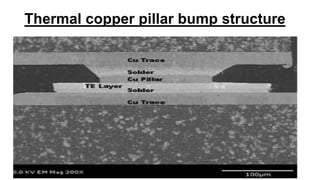
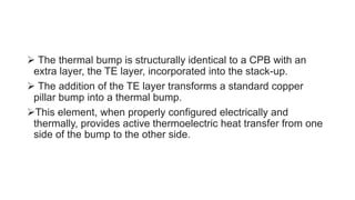
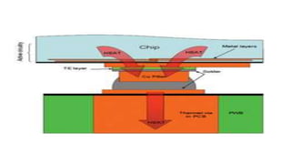
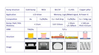
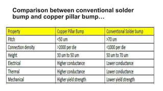
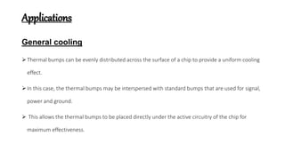
SEMINAR ON
Thermal copper pillar bump
GUIDED BY: PRESENTED BY:
SAJITH KUMAR S BIJITH DAS
CLASS NO. 25
20200387
Dept. of Electronics and communication
INTRODUCTION
• The thermal copper pillar bump, also known as the "thermal
bump", is a thermoelectric device made from thin-film
thermoelectric material embedded in flip chip interconnects for
use in electronics and optoelectronic packaging.
A brief history of solder and flip chip/chip scale
packaging.
• Solder bumping technology (the process of joining a chip to
a substrate without shorting using solder) was first conceived
and implemented by IBM in the early 1960s.
• The first was to embed copper balls in the solder bumps to
provide a positive stand-off.
• The bump provided a positive stand-off and was attached to the
substrate by means of solder that was screen-printed onto the
substrate.
Copper pillar solder bumping
• High-density interconnects have led to the use of copper pillar
solder bumps (CPB) for CPU and GPU packaging.
• CPBs are an attractive replacement for traditional solder bumps
because they provide a fixed stand-off independent of pitch.
• This is extremely important as most of the high-end products
are underfilled and a smaller standoff may create difficulties in
getting the underfill adhesive to flow under the die.
Thin-film thermoelectric technology
Thin films are thin material layers ranging from fractions of a nanometer to
several micrometers in thickness.
 Thin-film thermoelectric materials are grown by conventional
semiconductor deposition methods and fabricated using conventional
semiconductor micro-fabrication techniques.
Thin-film thermos electrics have been demonstrated to provide high heat
pumping capacity that far exceeds the capacities provided by traditional
bulk pellet TE products.
Intel Presler copper pillar solder bump
Thermal copper pillar bump
• The thermal bump is compatible with the existing flip-chip
manufacturing infrastructure.
• The result is higher performance and efficiency within the
existing semiconductor manufacturing paradigm.
• The thermal bump also enables power generating capabilities
within copper pillar bumps for energy recycling applications.
Thermal copper pillar bump structure
 The thermal bump is structurally identical to a CPB with an
extra layer, the TE layer, incorporated into the stack-up.
 The addition of the TE layer transforms a standard copper
pillar bump into a thermal bump.
This element, when properly configured electrically and
thermally, provides active thermoelectric heat transfer from one
side of the bump to the other side.
Comparison between conventional solder
bump and copper pillar bump…
Applications
General cooling
Thermal bumps can be evenly distributed across the surface of a chip to provide a uniform cooling
effect.
In this case, the thermal bumps may be interspersed with standard bumps that are used for signal,
power and ground.
 This allows the thermal bumps to be placed directly under the active circuitry of the chip for
maximum effectiveness.
Precision temperature control
Since thermal bumps can either cool or heat the chip depending on
the current direction, they can be used to provide precision control of
temperature for chips that must operate within specific temperature
ranges irrespective of ambient conditions.
For example, this is a common problem for many optoelectronic
components.
Power generation
In addition to chip cooling, thermal bumps can also be applied to high
heat-flux interconnects to provide a constant, steady source of power
for energy scavenging applications.
Such a source of power, typically in the mW range, can trickle charge
batteries for wireless sensor networks and other battery operated
systems.
Hotspot cooling
In microprocessors, graphics processors and other high-end chips,
hotspots can occur as power densities vary significantly across a chip.
These hotspots can severely limit the performance of the devices.
Benefit
Low cost
Lead free
Available with and without wafer re-passivation.
Superior Electro migration performance.
Qualified for advanced silicon node with low-k dielectrics.
Conclusion
Copper pillar bump technology is a fast emerging technology
for die to die bonding due to its several advantages over
conventional solder bump technology.
Fabrication labs and the semiconductor industry are looking
torwards adapting coppar pillar bumps for deep sub micron
technology chips due to its high reliability in high pin counts and
high packaging density.
Various innovations are going on to make copper pillar
technology more stable and more cost effective.
Thermal copper pillar bump.pptx

Thermal copper pillar bump.pptx

  • 1.
    SEMINAR ON Thermal copperpillar bump GUIDED BY: PRESENTED BY: SAJITH KUMAR S BIJITH DAS CLASS NO. 25 20200387 Dept. of Electronics and communication
  • 2.
    INTRODUCTION • The thermalcopper pillar bump, also known as the "thermal bump", is a thermoelectric device made from thin-film thermoelectric material embedded in flip chip interconnects for use in electronics and optoelectronic packaging.
  • 3.
    A brief historyof solder and flip chip/chip scale packaging. • Solder bumping technology (the process of joining a chip to a substrate without shorting using solder) was first conceived and implemented by IBM in the early 1960s. • The first was to embed copper balls in the solder bumps to provide a positive stand-off. • The bump provided a positive stand-off and was attached to the substrate by means of solder that was screen-printed onto the substrate.
  • 4.
    Copper pillar solderbumping • High-density interconnects have led to the use of copper pillar solder bumps (CPB) for CPU and GPU packaging. • CPBs are an attractive replacement for traditional solder bumps because they provide a fixed stand-off independent of pitch. • This is extremely important as most of the high-end products are underfilled and a smaller standoff may create difficulties in getting the underfill adhesive to flow under the die.
  • 5.
    Thin-film thermoelectric technology Thinfilms are thin material layers ranging from fractions of a nanometer to several micrometers in thickness.  Thin-film thermoelectric materials are grown by conventional semiconductor deposition methods and fabricated using conventional semiconductor micro-fabrication techniques. Thin-film thermos electrics have been demonstrated to provide high heat pumping capacity that far exceeds the capacities provided by traditional bulk pellet TE products.
  • 6.
    Intel Presler copperpillar solder bump
  • 7.
    Thermal copper pillarbump • The thermal bump is compatible with the existing flip-chip manufacturing infrastructure. • The result is higher performance and efficiency within the existing semiconductor manufacturing paradigm. • The thermal bump also enables power generating capabilities within copper pillar bumps for energy recycling applications.
  • 8.
    Thermal copper pillarbump structure
  • 9.
     The thermalbump is structurally identical to a CPB with an extra layer, the TE layer, incorporated into the stack-up.  The addition of the TE layer transforms a standard copper pillar bump into a thermal bump. This element, when properly configured electrically and thermally, provides active thermoelectric heat transfer from one side of the bump to the other side.
  • 12.
    Comparison between conventionalsolder bump and copper pillar bump…
  • 13.
    Applications General cooling Thermal bumpscan be evenly distributed across the surface of a chip to provide a uniform cooling effect. In this case, the thermal bumps may be interspersed with standard bumps that are used for signal, power and ground.  This allows the thermal bumps to be placed directly under the active circuitry of the chip for maximum effectiveness.
  • 14.
    Precision temperature control Sincethermal bumps can either cool or heat the chip depending on the current direction, they can be used to provide precision control of temperature for chips that must operate within specific temperature ranges irrespective of ambient conditions. For example, this is a common problem for many optoelectronic components.
  • 15.
    Power generation In additionto chip cooling, thermal bumps can also be applied to high heat-flux interconnects to provide a constant, steady source of power for energy scavenging applications. Such a source of power, typically in the mW range, can trickle charge batteries for wireless sensor networks and other battery operated systems.
  • 16.
    Hotspot cooling In microprocessors,graphics processors and other high-end chips, hotspots can occur as power densities vary significantly across a chip. These hotspots can severely limit the performance of the devices.
  • 17.
    Benefit Low cost Lead free Availablewith and without wafer re-passivation. Superior Electro migration performance. Qualified for advanced silicon node with low-k dielectrics.
  • 18.
    Conclusion Copper pillar bumptechnology is a fast emerging technology for die to die bonding due to its several advantages over conventional solder bump technology. Fabrication labs and the semiconductor industry are looking torwards adapting coppar pillar bumps for deep sub micron technology chips due to its high reliability in high pin counts and high packaging density. Various innovations are going on to make copper pillar technology more stable and more cost effective.