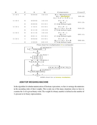
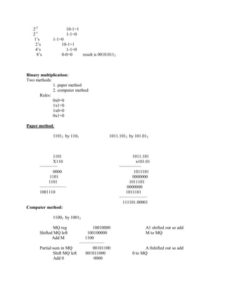
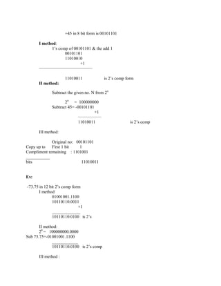
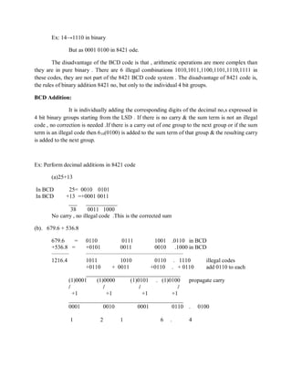
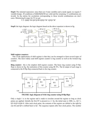
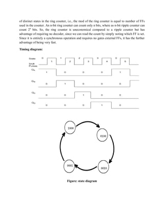
This document discusses number systems and binary logic. It begins by explaining the decimal number system and its positional weighting. It then introduces the binary number system, which uses only two symbols, 0 and 1, and also uses positional weighting. Key binary operations like addition, subtraction, multiplication and division are covered. Methods for converting between decimal and binary are provided. The document also discusses representing signed numbers in binary for computer arithmetic.


![NOR gate= Bubbled AND gate
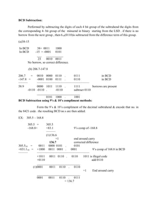
This can be extended to any variables.
(A+B+C+D+-----)‘=A‘B‘C‘D‘----
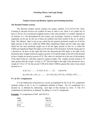
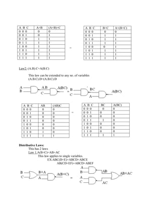
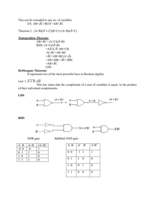
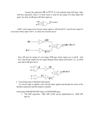
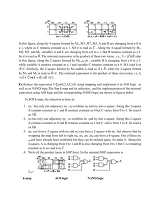
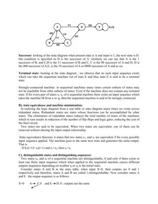
Law 2: (AB)‘=A‘+B‘
Complement of the product of variables is equal to the sum of their individual
components.
This law also can extend to any no. Of variables.
(ABCD---)‘=A‘+B‘+C‘+D‘+------
It can be extended to complicated expressions by
1. Complement the entire function
2. Change all the ANDs to ORS and all the Ors to ANDS
3. Complement each of the individual variables.
4. Change all 0s to 1s and 1s to 0s.
This procedure is called demorganization or complementation of switching expressions.
Shannon’s expansion Theorem:
This theorem states that any switching expression can be decomposed w.r.t. a
variable A into two parts, one containing A &other containing A‘. It is useful in decomposing
complex machines into an interconnection of smaller components.
f(A,B,C---)=A.f(1,B,C---)+A‘.f(0,B,C----)
f(A,B,C,---)=[A+f(0,B,C,-----)].[A‘+f(1,B,C-----]
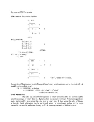
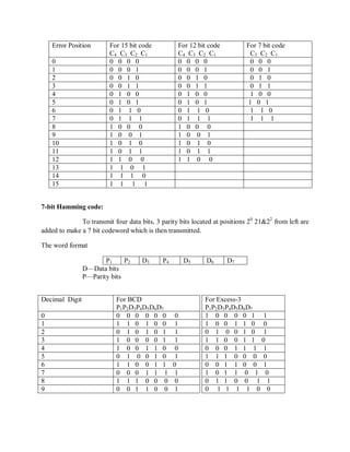
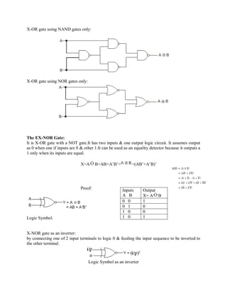
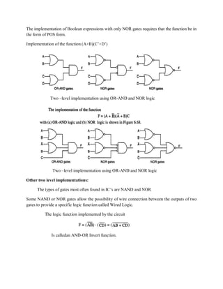
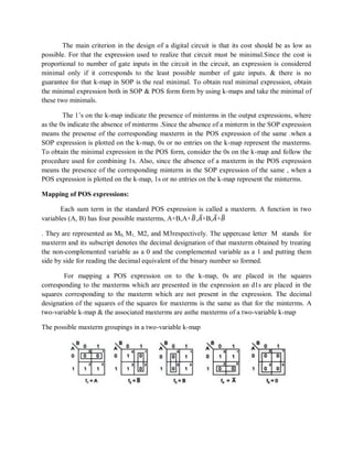
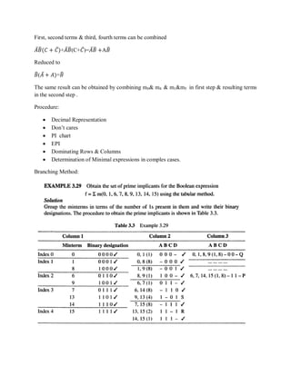
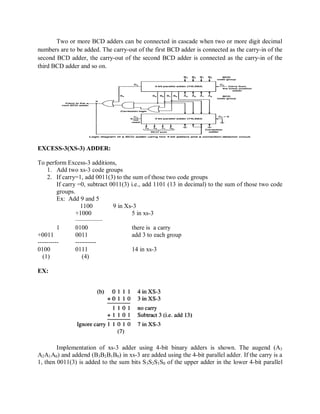
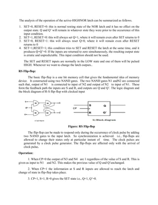
Ex: DeMorganize f=((A+B‘)(C+D‘))‘, f=((A+B‘)(C+D‘))‘
=(A+B‘)(C+D‘)
= A.B‘ +C.D‘
=A‘.B+C‘.D
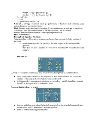
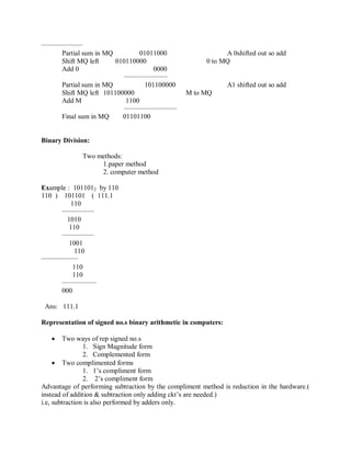
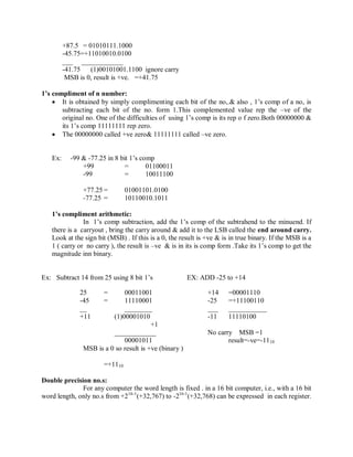
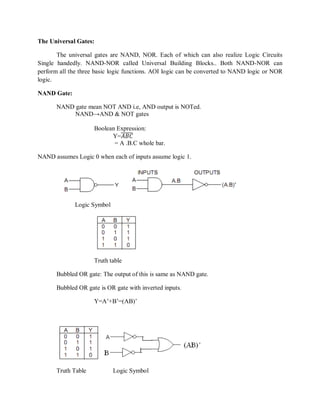
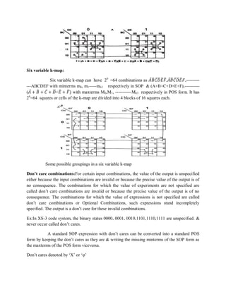
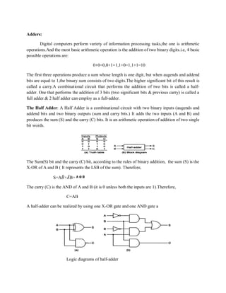
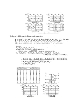
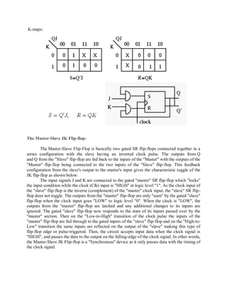
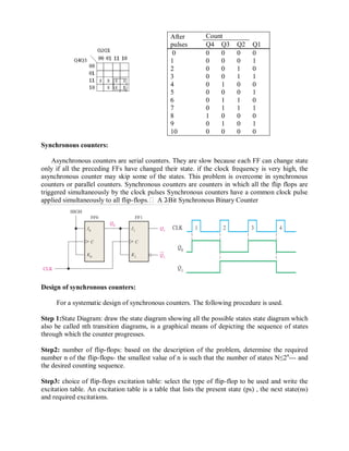
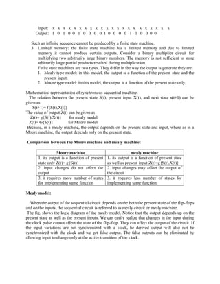
A B (AB)‘
0 0 1
0 1 1
1 0 1
1 1 0
A B A‘ B‘ A‘+B‘
0 0 1 1 1
0 1 1 0 1
1 0 0 1 1
1 1 0 0 0](https://image.slidesharecdn.com/scldnotes-160713173729/85/Switching-circuits-and-logic-design-39-320.jpg)
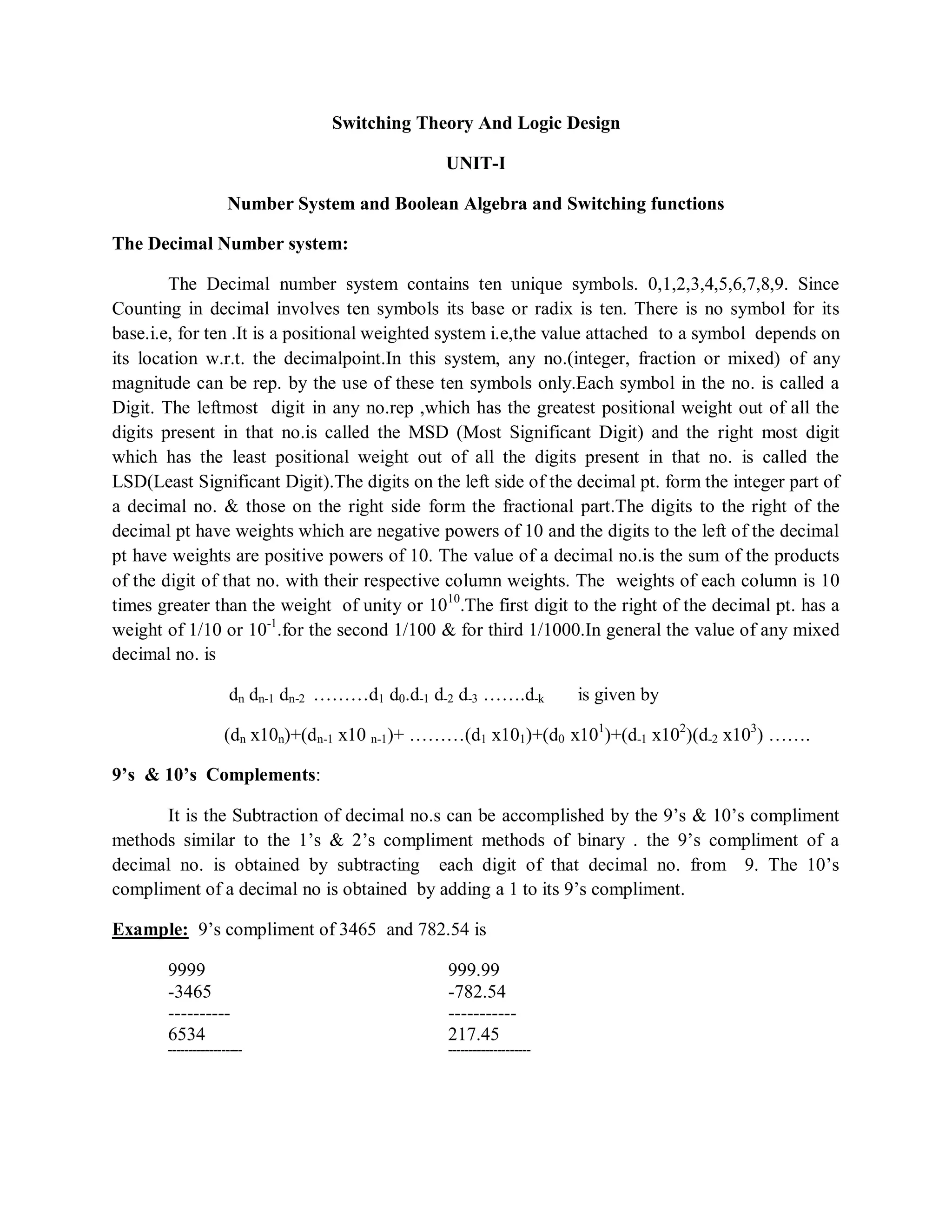
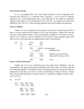
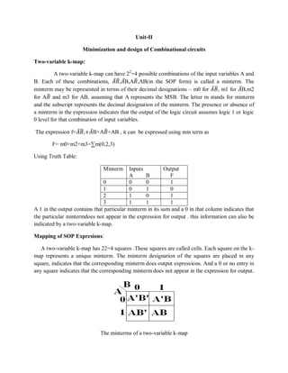
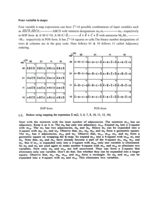
![Duality:
In a positive Logic system the more positive of the two voltage levels is represented by a
1 & the more negative by a 0. In a negative logic system the more positive of the two voltage
levels is represented by a 0 & more negative by a 1. This distinction between positive &negative
logic systems is important because an OR gate in the positive logic system becomes an AND
gate in the negative logic system &vice versa. Positive & Negative logics give a basic duality in
Boolean identities. Procedure dual identity by changing all ‗+‘ (OR) to ―.‘(AND) &
complementing all 0‘s &1‘s. Once a theorem or statement is proved, the dual also thus stands
proved called Principle of duality.
[f(A,B,C,-------0,1,+,.)]d =f(A,B,C,----1,0,.,+)
Relations between complement
(fc(A,B,C----)= (𝑓𝑐(𝐴. 𝐵, 𝐶 − −−)= (fd(𝐴, 𝐵, 𝐶,--)
(fd(A,B,C----)= (𝑓𝑐(𝐴. 𝐵, 𝐶 − −−)= (fc(𝐴, 𝐵, 𝐶,--)
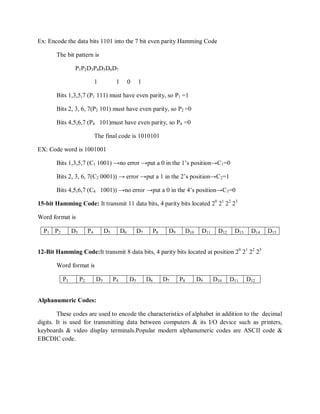
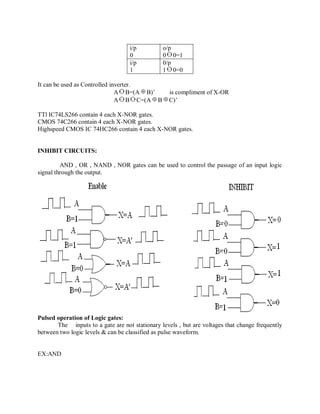
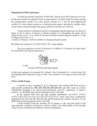
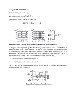
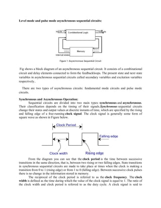
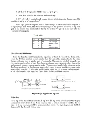
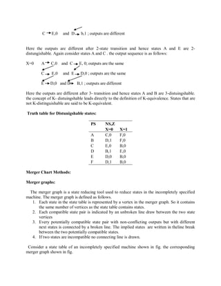
Duals:
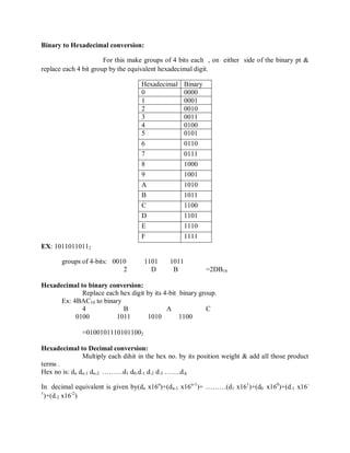
Expression Dual
0=1 1=0
0.1=0 1+0=1
0.0=0 1+1=1
1.1=1 0+0=0
A.0=0 A+1=1
A.1=A A+0=A
A.A=A A+A=A
A.𝐴=0 A+𝐴=1
A.B=B.A A+B=B+A
A.(B.C)=(A.B).C A+(B+C)=(A+B)+C
A.(B+C)=(AB+AC) A+BC=(A+B)(A+C)
A(A+B)=A A+AB=A
A.(A.B)=A.B A+A+B=A+B
𝐴𝐵=𝐴+𝐵 𝐴 + 𝐵=𝐴+𝐵
(A+B)(𝐴+C)(B+C)=(A+B)(𝐴+C) AB+𝐴C+BC=AB+𝐴C
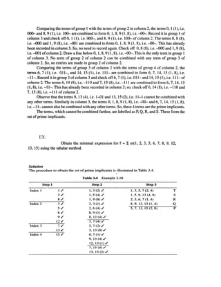
Reducing Boolean Expressions:
Procedure:
1. Multiply all variables necessary to remove parenthesis](https://image.slidesharecdn.com/scldnotes-160713173729/85/Switching-circuits-and-logic-design-40-320.jpg)

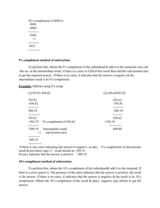
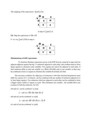
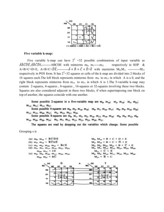
![Similarly NOR outputs of ECL gates can be tied together to form Wired NOR function.
The logic function implemented by this circuit is
Is called OR-AND INVERT Function.
EX: Open Collector TTL NAND gates, when tied together perform the wired AND logic is
called AOI
=(𝐴𝐵) .(𝐶𝐷)
=𝐴𝐵 + 𝐶𝐷
Similarly NOR outputs of ECL can tied together to perform a wired NOR function.
F=(𝐴 + 𝐵)+(𝐶 + 𝐷)
=[(𝐴 + 𝐵)(𝐶 + 𝐷)]
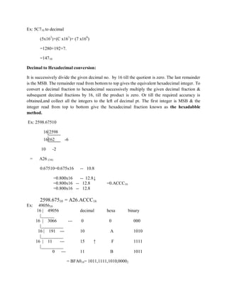
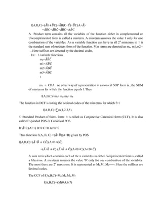
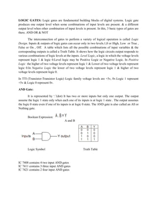
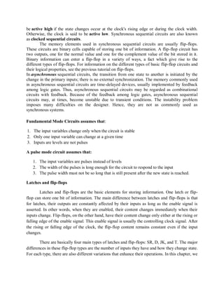
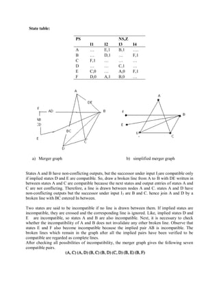
Non Degenerate forms:
Considering 4 types of gates AND, OR, NAND , NOR & assign one type of gate for
the first level & one type of gate for the second level. Find 16 possible combinations of two level
form. Eight of these are degenerate forms. Because they generate to a single operation. i.e, AND
gate in first level & AND gate in second The output is nearly the AND function of all input
variables.
The other non degenerate forms produce an implementation in SOP or POS are
AND-OR OR-AND
NAND-NAND NOR-NOR
NOR-OR NAND-NAND
OR-NAND AND-NOR](https://image.slidesharecdn.com/scldnotes-160713173729/85/Switching-circuits-and-logic-design-58-320.jpg)
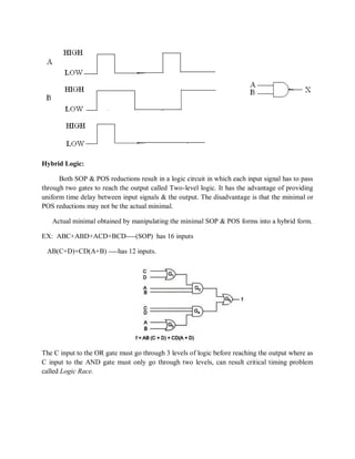
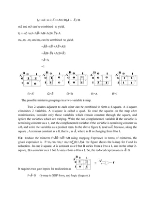
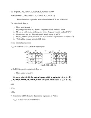
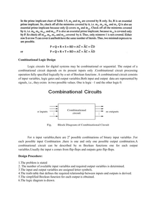
![The two forms are dual of each other.
AND-OR & OR-AND forms are the basic two-level forms.
NAND-NAND, NOR_NOR
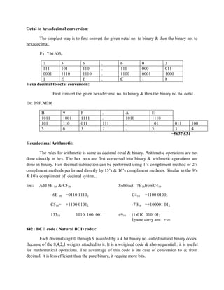
AOI Implementation:
The two forms Nandi-And and And-Nor perform AOI function.
Inversion isand-Nor form resembles the and-Or form done by the bubble in the output of the
NOR gate.
Its function is F= 𝐴𝐵 + 𝐶𝐷 + 𝐸
Two-level implementation in AND-NOR and NAND-AND form
OAI Implementation:
The twoforms OR-NAND and NOR-NOR perform OAI function.
OR-NAND form OR-AND form except inversion done by bubble in NAND gate.
Function F=[(𝐴 + 𝐵)(𝐶 + 𝐷)𝐸]](https://image.slidesharecdn.com/scldnotes-160713173729/85/Switching-circuits-and-logic-design-59-320.jpg)


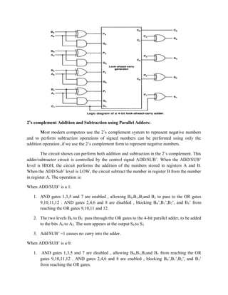
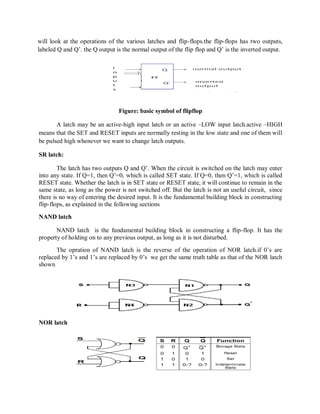
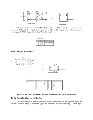
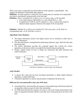
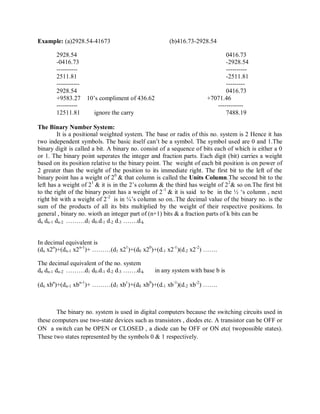
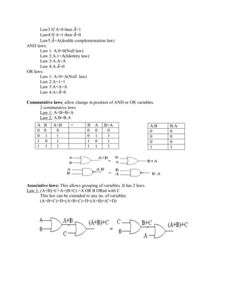
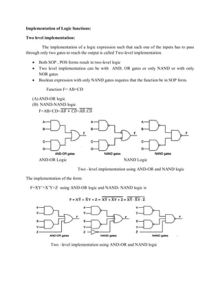
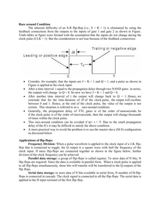
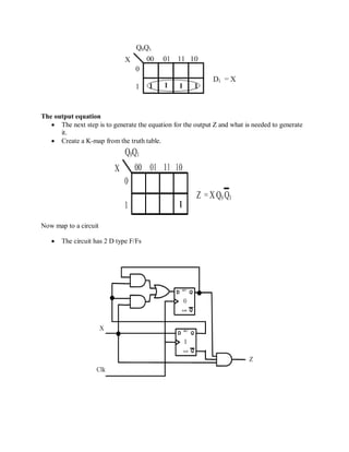
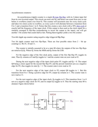
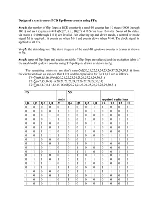
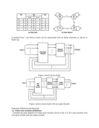
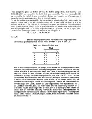
![JK flip-flop operation[28]
Characteristic table Excitation table
J K Qnext Comment Q Qnext J K Comment
0 0 Q hold state 0 0 0 X No change
0 1 0 reset 0 1 1 X Set
1 0 1 set 1 0 X 1 Reset
1 1 Q toggle 1 1 X 0 No change
T flip-flop:
If the T input is high, the T flip-flop changes state ("toggles") whenever the clock input is
strobed. If the T input is low, the flip-flop holds the previous value. This behavior is described by
the characteristic equation
Figure : symbol for T flip flop
(expanding the XOR operator
When T is held high, the toggle flip-flop divides the clock frequency by two; that is, if
clock frequency is 4 MHz, the output frequency obtained from the flip-flop will be 2 MHz This
"divide by" feature has application in various types of digital counters. A T flip-flop can also be
built using a JK flip-flop (J & K pins are connected together and act as T) or D flip-flop (T input
and Previous is connected to the D input through an XOR gate).](https://image.slidesharecdn.com/scldnotes-160713173729/85/Switching-circuits-and-logic-design-118-320.jpg)
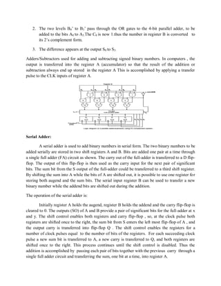
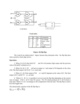
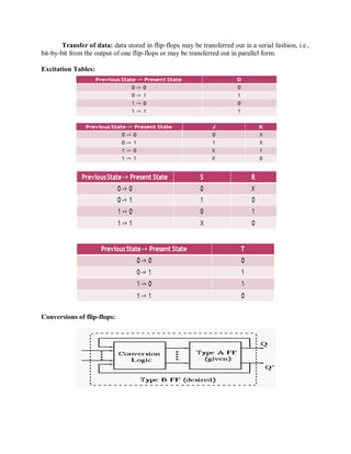
![T flip-flop operation[28]
Characteristic table Excitation table
Comment Comment
0 0 0 hold state (no clk) 0 0 0 No change
0 1 1 hold state (no clk) 1 1 0 No change
1 0 1 toggle 0 1 1 Complement
1 1 0 toggle 1 0 1 Complement
Flip flop operating characteristics:
The operation characteristics specify the performance, operating requirements, and
operating limitations of the circuits. The operation characteristics mentions here apply to all flip-
flops regardless of the particular form of the circuit.
Propagation Delay Time: is the interval of time required after an input signal has been applied
for the resulting output change to occur.
Set-up Time: is the minimum interval required for the logic levels to be maintained constantly
on the inputs (J and K, or S and R, or D) prior to the triggering edge of the clock pulse in order
for the levels to be reliably clocked into the flip-flop.
Hold Time: is the minimum interval required for the logic levels to remain on the inputs after
the triggering edge of the clock pulse in order for the levels to be reliably clocked into the flip-
flop.
Maximum Clock Frequency: is the highest rate that a flip-flop can be reliably triggered.
Power Dissipation: is the total power consumption of the device. It is equal to product of supply
voltage (Vcc) and the current (Icc).
P=Vcc.Icc
The power dissipation of a flip flop is usually in mW.
Pulse Widths: are the minimum pulse widths specified by the manufacturer for the Clock, SET
and CLEAR inputs.
Clock transition times: for reliable triggering, the clock waveform transition times should be
kept very short. If the clock signal takes too long to make the transitions from one level to other,
the flip flop may either triggering erratically or not trigger at all.](https://image.slidesharecdn.com/scldnotes-160713173729/85/Switching-circuits-and-logic-design-119-320.jpg)

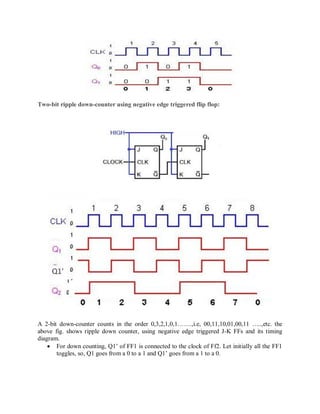
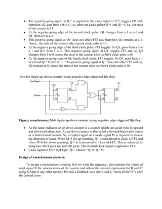
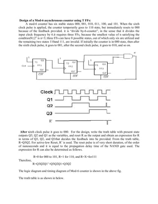
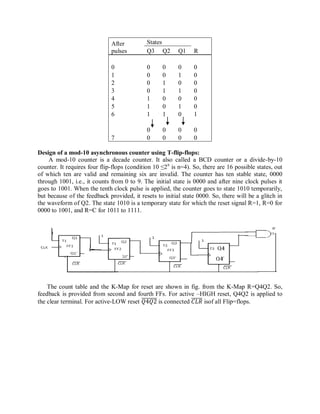

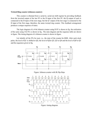

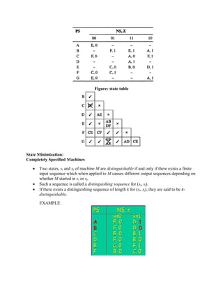
![Theorem. For every machine M there is a minimum machine Mred ~ M. Mred is unique up to
isomorphism.
State Minimization of CSMs: Complexity
Algorithm DFA ~ DFAmin
Input: A finite automaton M = (Q, , , q 0, F ) with no unreachable states.
Output: A minimum finite automaton M‘ = (Q’, , ‘, q ‘0, F’ ).
Method:
1. t :=2; Q0:= { undefined }; Q1:=F; Q2:= QF.
2. while there is 0 < i t, a with (Qi,a) Qj, for all j t
do (a) Choose such an i, a , and j t with (Qi,a) Qj .
(b) Qt +1 := {q Qi | (q,a) Qj };
Qi := Qi Qt +1;
t := t +1.
end.
3. (* Denote [q ] the equivalence class of state q , and {Qi } the set of all equivalence
classes. *)
Q’ := {Q1, Q2, ..., Qt }.
q ‘0 := [q0].
F’ := { [q] Q’ | q F }.
’ ( [q], a) := [(q,a)] for all q Q, a .
Standard implementation: O (kn 2
), where n =|Q| and k = ||
Modification of the body of the while loop:
1. Choose such an i, a , and choose j1,j2 t with j1 j2, (Qi,a) Qj1 , and
(Qi,a) Qj2 .
2. If |{q Qi | (q,a) Qj1}| |{q Qi | (q,a) Qj2}|](https://image.slidesharecdn.com/scldnotes-160713173729/85/Switching-circuits-and-logic-design-165-320.jpg)