- Inorganic solid state chemistry deals with defects in solids like point defects and non-stoichiometry. There are two main types of point defects - Schottky defects and Frenkel defects.
- Schottky defects involve a pair of cation and anion vacancies while Frenkel defects occur when an ion moves into an interstitial site, leaving a vacancy.
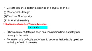
- Defects influence properties like mechanical strength, electrical conductivity and chemical reactivity. The number of defects increases with temperature according to an equation involving defect formation energy.
- Non-stoichiometric compounds have a varying ratio of cations to anions and can involve metal excess or deficiency defects involving interstitial