The document describes several digital and analog layout projects completed using Cadence tools including Virtuoso Layout Editor and Assura Verification. For digital projects, standard cells like inverters and logic gates were designed using a 130nm TSMC process. Analog projects included a level shifter, operational amplifier, band gap reference, DAC, and PLL. Challenges involved routing with tight metal pitches, transistor matching, reducing parasitics, and separating analog and digital blocks to prevent noise transfer.
Note : To get more understanding Recommending to see first section - Low power in vlsi with upf basics part 1
With Increase in Portable devices, VLSI chips has to consider about Power usages in VLSI silicon chips. So Power Aware design and verification is so important in Industry. To get basic knowledge on Low Power Design and Verification with UPF basics Go through this Slides.
This paper proposes fault location model for underground power cable using microcontroller. The aim of this project is to determine the di stance of underground cable fault from base station in kilometers. This project uses the simple c oncept of ohm�s law.When any fault like short circuit occurs,voltage drop will vary depending on the length of fault in cable,since the current varies. A set of resistors are ther efore used to represen t the cable and a dc vol tage is fed at one end and the fault is detected by detecting the change in voltage using a analog to voltage converter and a microcontroller is used to make the necessary calculations so that the fault distance is displayed on the LCD display.
With Increase in Portable devices, VLSI chips has to consider about Power usages in VLSI silicon chips. So Power Aware design and verification is so important in Industry. To get basic knowledge on Low Power Design and Verification with UPF basics Go through this Slides.
Design and Implementation of Refresh and Timing Controller Unit for LPDDR2 Me...Editor IJCATR
this paper presents a “Implementation of “Refresh And Timing Controller” unit for low power double data rate 2 memory
controller (LPDDR2 MEMORY CONTROLLER). “Refresh and Timing Controller” unit plays a vital role for LPDDR2 memory
controller .It maintains different timing parameters to handle various commands for memory like refresh, read and write operations and
also performs Memory Initialization. Since it is low power DDR2 the maximum duration in power-down mode and deep power down
mode is maintained by “Refresh and Timing Controller” unit. The refresh rate period is programmable using the Refresh Period
Register. It supports “All Bank Refresh”. The unit has timers to accommodate Refresh, Read/Write, and Power down modes. The RTL
is done using the System Verilog. The design is simulated
IJRET : International Journal of Research in Engineering and Technology is an international peer reviewed, online journal published by eSAT Publishing House for the enhancement of research in various disciplines of Engineering and Technology. The aim and scope of the journal is to provide an academic medium and an important reference for the advancement and dissemination of research results that support high-level learning, teaching and research in the fields of Engineering and Technology. We bring together Scientists, Academician, Field Engineers, Scholars and Students of related fields of Engineering and Technology
Vlsi design process for low power design methodology using reconfigurable fpgaeSAT Publishing House
IJRET : International Journal of Research in Engineering and Technology is an international peer reviewed, online journal published by eSAT Publishing House for the enhancement of research in various disciplines of Engineering and Technology. The aim and scope of the journal is to provide an academic medium and an important reference for the advancement and dissemination of research results that support high-level learning, teaching and research in the fields of Engineering and Technology. We bring together Scientists, Academician, Field Engineers, Scholars and Students of related fields of Engineering and Technology.
three phase fault analysis with auto reset for temporary fault and trip for p...Vikram Rawani
The project was aimed to prevent failures due to some faults which can be temporary or permanent in 3-phase power supply .
The purpose of our project was to develop an automatic tripping mechanism for the three phase supply system. The project output resets automatically after a brief interruption in the event temporary fault while it remains in tripped condition in case of permanent fault.
This project was done under Dr Jason Hogan in Professor Mark Kasevich's lab at Stanford in Summer 2014. Using KICAD, I developed and designed an intelligent customizable PCB in order to shield the lab's devices and equipment from anomalies, disruptions and surges in the power supply.
Improved Grid Synchronization Algorithm for DG System using DSRF PLL under Gr...IJERA Editor
Distributed Generation (DG) System is a small scale electric power generation at or near the user’s facility as
opposed to the normal mode of centralized power generation. In order to ensure safe and reliable operation of
power system based on DS, grid synchronization algorithm plays a very important role. This paper presents a
Double Synchronous Reference Frame (DSRF) phase locked loop (PLL) based on synthesis circuit for grid
synchronization of distributed generation (DG) system under grid disturbances aimed to provide an estimation
of the angular frequency and both the positive and negative sequences of the fundamental component of an
unbalanced three-phase signal. The design of this PLL is based on a complete description of the source voltage
involving both positive and negative sequences in stationary coordinates and considering the angular frequency
as an uncertain parameter.
International Journal of Engineering Research and DevelopmentIJERD Editor
Electrical, Electronics and Computer Engineering,
Information Engineering and Technology,
Mechanical, Industrial and Manufacturing Engineering,
Automation and Mechatronics Engineering,
Material and Chemical Engineering,
Civil and Architecture Engineering,
Biotechnology and Bio Engineering,
Environmental Engineering,
Petroleum and Mining Engineering,
Marine and Agriculture engineering,
Aerospace Engineering.
final Year Projects, Final Year Projects in Chennai, Software Projects, Embedded Projects, Microcontrollers Projects, DSP Projects, VLSI Projects, Matlab Projects, Java Projects, .NET Projects, IEEE Projects, IEEE 2009 Projects, IEEE 2009 Projects, Software, IEEE 2009 Projects, Embedded, Software IEEE 2009 Projects, Embedded IEEE 2009 Projects, Final Year Project Titles, Final Year Project Reports, Final Year Project Review, Robotics Projects, Mechanical Projects, Electrical Projects, Power Electronics Projects, Power System Projects, Model Projects, Java Projects, J2EE Projects, Engineering Projects, Student Projects, Engineering College Projects, MCA Projects, BE Projects, BTech Projects, ME Projects, MTech Projects, Wireless Networks Projects, Network Security Projects, Networking Projects, final year projects, ieee projects, student projects, college projects, ieee projects in chennai, java projects, software ieee projects, embedded ieee projects, "ieee2009projects", "final year projects", "ieee projects", "Engineering Projects", "Final Year Projects in Chennai", "Final year Projects at Chennai", Java Projects, ASP.NET Projects, VB.NET Projects, C# Projects, Visual C++ Projects, Matlab Projects, NS2 Projects, C Projects, Microcontroller Projects, ATMEL Projects, PIC Projects, ARM Projects, DSP Projects, VLSI Projects, FPGA Projects, CPLD Projects, Power Electronics Projects, Electrical Projects, Robotics Projects, Solor Projects, MEMS Projects, J2EE Projects, J2ME Projects, AJAX Projects, Structs Projects, EJB Projects, Real Time Projects, Live Projects, Student Projects, Engineering Projects, MCA Projects, MBA Projects, College Projects, BE Projects, BTech Projects, ME Projects, MTech Projects, M.Sc Projects, Final Year Java Projects, Final Year ASP.NET Projects, Final Year VB.NET Projects, Final Year C# Projects, Final Year Visual C++ Projects, Final Year Matlab Projects, Final Year NS2 Projects, Final Year C Projects, Final Year Microcontroller Projects, Final Year ATMEL Projects, Final Year PIC Projects, Final Year ARM Projects, Final Year DSP Projects, Final Year VLSI Projects, Final Year FPGA Projects, Final Year CPLD Projects, Final Year Power Electronics Projects, Final Year Electrical Projects, Final Year Robotics Projects, Final Year Solor Projects, Final Year MEMS Projects, Final Year J2EE Projects, Final Year J2ME Projects, Final Year AJAX Projects, Final Year Structs Projects, Final Year EJB Projects, Final Year Real Time Projects, Final Year Live Projects, Final Year Student Projects, Final Year Engineering Projects, Final Year MCA Projects, Final Year MBA Projects, Final Year College Projects, Final Year BE Projects, Final Year BTech Projects, Final Year ME Projects, Final Year MTech Projects, Final Year M.Sc Projects, IEEE Java Projects, ASP.NET Projects, VB.NET Projects, C# Projects, Visual C++ Projects, Matlab Projects, NS2 Projects, C Projects, Microcontroller Projects, ATMEL Projects, PIC Projects, ARM Projects, DSP Projects, VLSI Projects, FPGA Projects, CPLD Projects, Power Electronics Projects, Electrical Projects, Robotics Projects, Solor Projects, MEMS Projects, J2EE Projects, J2ME Projects, AJAX Projects, Structs Projects, EJB Projects, Real Time Projects, Live Projects, Student Projects, Engineering Projects, MCA Projects, MBA Projects, College Projects, BE Projects, BTech Projects, ME Projects, MTech Projects, M.Sc Projects, IEEE 2009 Java Projects, IEEE 2009 ASP.NET Projects, IEEE 2009 VB.NET Projects, IEEE 2009 C# Projects, IEEE 2009 Visual C++ Projects, IEEE 2009 Matlab Projects, IEEE 2009 NS2 Projects, IEEE 2009 C Projects, IEEE 2009 Microcontroller Projects, IEEE 2009 ATMEL Projects, IEEE 2009 PIC Projects, IEEE 2009 ARM Projects, IEEE 2009 DSP Projects, IEEE 2009 VLSI Projects, IEEE 2009 FPGA Projects, IEEE 2009 CPLD Projects, IEEE 2009 Power Electronics Projects, IEEE 2009 Electrical Projects, IEEE 2009 Robotics Projects, IEEE 2009 Solor Projects, IEEE 2009 MEMS Projects, IEEE 2009 J2EE P
International Journal of Engineering Research and Applications (IJERA) is an open access online peer reviewed international journal that publishes research and review articles in the fields of Computer Science, Neural Networks, Electrical Engineering, Software Engineering, Information Technology, Mechanical Engineering, Chemical Engineering, Plastic Engineering, Food Technology, Textile Engineering, Nano Technology & science, Power Electronics, Electronics & Communication Engineering, Computational mathematics, Image processing, Civil Engineering, Structural Engineering, Environmental Engineering, VLSI Testing & Low Power VLSI Design etc.
We are occupied in providing Reyrolle 7SR11 The offered product is extremely admired by our patrons for its top performance and longer working life.;
Features:
High performance
Long functional life
Easy to use
Longer life service
Compact structure
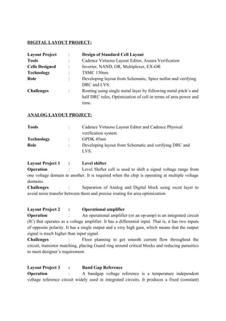
1. DIGITAL LAYOUT PROJECT:
Layout Project : Design of Standard Cell Layout
Tools : Cadence Virtuoso Layout Editor, Assura Verification
Cells Designed : Inverter, NAND, OR, Multiplexer, EX-OR
Technology : TSMC 130nm
Role : Developing layout from Schematic, Spice netlist and verifying
DRC and LVS.
Challenges : Routing using single metal layer by following metal pitch’s and
half DRC rules, Optimization of cell in terms of area power and
time.
ANALOG LAYOUT PROJECT:
Tools : Cadence Virtuoso Layout Editor and Cadence Physical
verification system
Technology : GPDK 45nm
Role : Developing layout from Schematic and verifying DRC and
LVS.
Layout Project 1 : Level shifter
Operation : Level Shifter cell is used to shift a signal voltage range from
one voltage domain to another. It is required when the chip is operating at multiple voltage
domains.
Challenges : Separation of Analog and Digital block using sxcut layer to
avoid noise transfer between them and precise routing for area optimization.
Layout Project 2 : Operational amplifier
Operation : An operational amplifier (or an op-amp) is an integrated circuit
(IC) that operates as a voltage amplifier. It has a differential input. That is, it has two inputs
of opposite polarity. It has a single output and a very high gain, which means that the output
signal is much higher than input signal.
Challenges : Floor planning to get smooth current flow throughout the
circuit, transistor matching, placing Guard ring around critical blocks and reducing parasitics
to meet designer’s requirement.
Layout Project 3 : Band Gap Reference
Operation : A bandgap voltage reference is a temperature independent
voltage reference circuit widely used in integrated circuits. It produces a fixed (constant)
2. voltage regardless of power supply variations, temperature changes and circuit loading from a
device.
Challenges : Floor planning, Resistor matching, BJT matching, adding
dummies properly to avoid STI effect and maintaining EM rules
Layout Project 4 : DAC (Digital to Analog Converter)
Operation : DAC is a device used to convert digital signal into analog
signal based on R-2R ladder network and the switches.
Challenges : R-2R ladder network matching, following EM rules for given
current ratings throughout the circuit, Hierarchical Design and maintaining equal and shortest
routing between each switch and R-2R ladder for reliable output.
Layout Project 5 : PLL (Phase Locked Loop)
Operation : A phase-locked loop (PLL) is an electronic circuit with a voltage or
voltage-driven oscillator that constantly adjusts to match the frequency of an input signal. PLLs are
used to generate, stabilize, modulate, demodulate, filter or recover a signal from a "noisy"
communications channel where data has been interrupted
Challenges : Floor planning according to the size of inductor such that
smooth current flows with optimized area, VCO matching, shielding critical nets,
Maintaining less parasitic and reducing STI and EMI effects