Semiconductors
•
7 likes•798 views

Semiconductors & Rectifiers by Prof. K. Adisesha Notes

More Related Content
What's hot
What's hot (20)
Similar to Semiconductors
Similar to Semiconductors (20)
More from Prof. Dr. K. Adisesha
More from Prof. Dr. K. Adisesha (20)
Recently uploaded
Recently uploaded (20)
Semiconductors
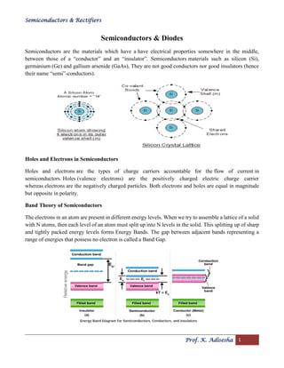
- 1. Semiconductors & Rectifiers Prof. K. Adisesha 1 Semiconductors & Diodes Semiconductors are the materials which have a have electrical properties somewhere in the middle, between those of a “conductor” and an “insulator”. Semiconductors materials such as silicon (Si), germanium (Ge) and gallium arsenide (GaAs), They are not good conductors nor good insulators (hence their name “semi”-conductors). Holes and Electrons in Semiconductors Holes and electrons are the types of charge carriers accountable for the flow of current in semiconductors. Holes (valence electrons) are the positively charged electric charge carrier whereas electrons are the negatively charged particles. Both electrons and holes are equal in magnitude but opposite in polarity. Band Theory of Semiconductors The electrons in an atom are present in different energy levels. When we try to assemble a lattice of a solid with N atoms, then each level of an atom must split up into N levels in the solid. This splitting up of sharp and tightly packed energy levels forms Energy Bands. The gap between adjacent bands representing a range of energies that possess no electron is called a Band Gap.
- 2. Semiconductors & Rectifiers Prof. K. Adisesha 2 Conduction Band and Valence Band in Semiconductors Valence Band: The energy band involving the energy levels of valence electrons is known as the valence band. It is the highest occupied energy band. When compared with insulators, the bandgap in semiconductors is smaller. It allows the electrons in the valence band to jump into the conduction band on receiving any external energy. Conduction Band: It is the lowest unoccupied band that includes the energy levels of positive (holes) or negative (free electrons) charge carriers. It has conducting electrons resulting in the flow of current. The conduction band possess high energy level and are generally empty. The conduction band in semiconductors accepts the electrons from the valence band. Properties of Semiconductors are: ➢ Semiconductor acts like an insulator at Zero Kelvin. On increasing the temperature, it works as a conductor. ➢ Due to their exceptional electrical properties, semiconductors can be modified by doping to make semiconductor devices suitable for energy conversion, switches, and amplifiers. ➢ Lesser power losses. ➢ Semiconductors are smaller in size and possess less weight. ➢ Their resistivity is higher than conductors but lesser than insulators. ➢ The resistance of semiconductor materials decreases with the increase in temperature and vice- versa. Types of Semiconductors Semiconductors can be classified as: ➢ Intrinsic Semiconductor ➢ Extrinsic Semiconductor
- 3. Semiconductors & Rectifiers Prof. K. Adisesha 3 Intrinsic Semiconductor An intrinsic type of semiconductor material is made to be very pure chemically. It is made up of only a single type of element. Germanium (Ge) and Silicon (Si) are the most common type of intrinsic semiconductor elements. They have four valence electrons (tetravalent). They are bound to the atom by covalent bond at absolute zero temperature. When the temperature rises, due to collisions, few electrons are unbounded and become free to move through the lattice, thus creating an absence in its original position (hole). These free electrons and holes contribute to the conduction of electricity in the semiconductor. The negative and positive charge carriers are equal in number. Energy Band Diagram of Intrinsic Semiconductor The energy band diagram of an intrinsic semiconductor is shown below: In intrinsic semiconductors, current flows due to the motion of free electrons as well as holes. The total current is the sum of the electron current Ie due to thermally generated electrons and the hole current Ih
- 4. Semiconductors & Rectifiers Prof. K. Adisesha 4 Total Current (I) = Ie + Ih For an intrinsic semiconductor, at finite temperature, the probability of electrons to exist in conduction band decreases exponentially with increasing bandgap (Eg) n = n0e-Eg/2.Kb.T Where, Eg = Energy bandgap Kb = Boltzmann’s constants Extrinsic Semiconductor The conductivity of semiconductors can be greatly improved by introducing a small number of suitable replacement atoms called IMPURITIES. The process of adding impurity atoms to the pure semiconductor is called DOPING. Usually, only 1 atom in 107 is replaced by a dopant atom in the doped semiconductor. An extrinsic semiconductor can be further classified into: ➢ N-type Semiconductor ➢ P-type Semiconductor Classification of Extrinsic Semiconductor N-Type Semiconductor When a pure semiconductor (Silicon or Germanium) is doped by pentavalent impurity Antimony (symbol Sb) as well as Phosphorus (symbol P) then, four electrons out of five valence electrons bonds with the four electrons of Ge or Si. The fifth electron of the dopant is set free. Thus, the impurity atom donates a free electron for conduction in the lattice and is called “Donar“.
- 5. Semiconductors & Rectifiers Prof. K. Adisesha 5 Since the number of free electron increases by the addition of an impurity, the negative charge carriers increase. Hence, it is called n-type semiconductor. Crystal as a whole is neutral, but the donor atom becomes an immobile positive ion. As conduction is due to a large number of free electrons, the electrons in the n-type semiconductor are the MAJORITY CARRIERS and holes are the MINORITY CARRIERS. P-Type Semiconductor When a pure semiconductor is doped with a trivalent impurity (B, Al, In, Ga ) then, the three valence electrons of the impurity bonds with three of the four valence electrons of the semiconductor. This leaves an absence of electron (hole) in the impurity. These impurity atoms which are ready to accept bonded electrons are called “Acceptors“. With the increase in the number of impurities, holes (the positive charge carriers) are increased. Hence, it is called p-type semiconductor. Crystal as a whole is neutral, but the acceptors become an immobile negative ion. As conduction is due to a large number of holes, the holes in the p-type semiconductor are MAJORITY CARRIERS and electrons are MINORITY CARRIERS. Difference Between Intrinsic and Extrinsic Semiconductors Intrinsic Semiconductor Extrinsic Semiconductor Pure semiconductor Impure semiconductor Density of electrons is equal to the density of holes Density of electrons is not equal to the density of holes Electrical conductivity is low Electrical conductivity is high Dependence on temperature only Dependence on temperature as well as on the amount of impurity No impurities Trivalent impurity, pentavalent impurity Applications of Semiconductors Let us now understand the uses of semiconductors in daily life. Semiconductors are used in almost all electronic devices. Without them, our life would be much different. Their reliability, compactness, low cost and controlled conduction of electricity make them ideal to be used for various purposes in a wide range of components and devices. Transistors, diodes, photosensors, microcontrollers, integrated chips and much more are made up of semiconductors.
- 6. Semiconductors & Rectifiers Prof. K. Adisesha 6 PN Junction Diode A PN-junction diode is formed when a p-type semiconductor is fused to an n-type semiconductor creating a potential barrier voltage across the diode junction When the N-type semiconductor and P-type semiconductor materials are first joined together, resulting that some of the free electrons from the donor impurity atoms begin to migrate across this newly formed junction. This charge transfer of electrons and holes across the PN junction is known as diffusion. This area around the PN Junction is now called the Depletion Layer. Biasing: If an external potential is applied to the terminals of PN junction, it will alter the potential between the P and N-regions. This potential difference can alter the flow of majority carriers, so that the PN junction can be used as an opportunity for the diffusion of electrons and holes. Biasing conditions for the Junction Diode are: ➢ Forward Bias: External voltage decreases the built-in potential barrier. ➢ Reverse Bias: External voltage increases the built-in potential barrier. ➢ Zero Bias: No external voltage is applied. V-I Characteristics of PN Junction Diode VI characteristics of PN junction diode is a curve between the voltage and current through the circuit. Voltage is taken along the x-axis while the current is taken along the y-axis. The graph is the VI
- 7. Semiconductors & Rectifiers Prof. K. Adisesha 7 characteristics curve of the PN junction diode. With the help of the curve we can understand that there are three regions in which the diode works, and they are: ➢ Zero bias ➢ Forward bias ➢ Reverse bias Junction Diode Summary The PN junction region of a Junction Diode has the following important characteristics: ➢ Semiconductors contain two types of mobile charge carriers, “Holes” and “Electrons”. ➢ The holes are positively charged while the electrons negatively charged. ➢ A semiconductor may be doped with donor impurities such as Antimony (N-type doping), so that it contains mobile charges which are primarily electrons. ➢ A semiconductor may be doped with acceptor impurities such as Boron (P-type doping), so that it contains mobile charges which are mainly holes. ➢ The junction region itself has no charge carriers and is known as the depletion region. ➢ The junction (depletion) region has a physical thickness that varies with the applied voltage. ➢ When a diode is Zero Biased no external energy source is applied and a natural Potential Barrier is developed across a depletion layer which is approximately 0.5 to 0.7v for silicon diodes and approximately 0.3 of a volt for germanium diodes. ➢ When a junction diode is Forward Biased the thickness of the depletion region reduces and the diode acts like a short circuit allowing full circuit current to flow. ➢ When a junction diode is Reverse Biased the thickness of the depletion region increases and the diode acts like an open circuit blocking any current flow, (only a very small leakage current will flow).
- 8. Semiconductors & Rectifiers Prof. K. Adisesha 8 Rectifiers A rectifier is an electrical component that converts alternating current (AC) to direct current (DC). A rectifier is analogous to a one-way valve that allows an electrical current to flow in only one direction. The process of converting AC current to DC current is known as rectification. A rectifier can take several physical forms such as solid-state diodes, vacuum tube diodes, mercury-arc valves, silicon-controlled rectifiers, and various other silicon-based semiconductor switches. Defining Half Wave Rectifier Half-wave rectifiers transform AC voltage to DC voltage. A halfwave rectifier circuit uses only one diode for the transformation. A halfwave rectifier is defined as a type of rectifier that allows only one-half cycle of an AC voltage waveform to pass while blocking the other half cycle. Half Wave Rectifier Circuit A half-wave rectifier is the simplest form of the rectifier and requires only one diode for the construction of a half wave rectifier circuit. A half wave rectifier circuit consists of three main components as follows: ➢ A diode ➢ A transformer ➢ A resistive load Given below is the half-wave rectifier diagram: Working of Half Wave Rectifier In this section, let us understand how a half-wave rectifier transforms AC into DC. 1. A high AC voltage is applied to the primary side of the step-down transformer. The obtained secondary low voltage is applied to the diode. 2. The diode is forward biased during the positive half cycle of the AC voltage and reversed biased during the negative half cycle. 3. The final output voltage waveform is as shown in the figure below:
- 9. Semiconductors & Rectifiers Prof. K. Adisesha 9 Half Wave Rectifier Formula Ripple Factor of Half Wave Rectifier Ripple factor determines how well a halfwave rectifier can convert AC voltage to DC voltage. Ripple factor can be quantified using the following formula: The ripple factor of a half wave rectifier is 1.21. Efficiency of Halfwave rectifier The efficiency of a half wave rectifier is the ratio of output DC power to the input AC power. The efficiency formula for half wave rectifier is given as follows; RMS value of Half Wave Rectifier The RMS value of the load current for a half-wave rectifier is given by the formula: Form factor of a Halfwave Rectifier The form factor is the ratio between RMS value and average value and is given by the formula:
- 10. Semiconductors & Rectifiers Prof. K. Adisesha 10 Applications of Half Wave Rectifier Here are a few common applications of half wave rectifiers: • They used for signal demodulation purpose • They are used for rectification applications • They are used for signal peak applications Disadvantages of Half Wave Rectifier • Power loss • Low output voltage • The output contains a lot of ripples Full Wave Rectifiers A full wave rectifier is defined as a rectifier that converts the complete cycle of alternating current into pulsating DC. Unlike half wave rectifiers that utilize only the half wave of the input AC cycle, full wave rectifiers utilize the full cycle. The lower efficiency of the half wave rectifier can be overcome by the full wave rectifier. The full wave rectifier circuit can be constructed in two ways: ➢ Centre tapped full wave rectifier. ➢ Bridge rectifier. Working of Centre tapped full wave rectifier The input AC supplied to the full wave rectifier is very high. The step-down transformer in the rectifier circuit converts the high voltage AC into low voltage AC. The anode of the centre tapped diodes is connected to the secondary winding of the transformer and also connected to the load resistor. During the positive half cycle of the alternating current, the top half of the secondary winding becomes positive while the second half of the secondary winding becomes negative. During the positive half cycle, diode D1 is forward biased as it is connected to the top of the secondary winding while diode D2 is reverse biased as it is connected to the bottom of the secondary winding. Due to this, diode D1 will conduct acting as a short circuit and D2 will not conduct acting as an open circuit
- 11. Semiconductors & Rectifiers Prof. K. Adisesha 11 During the negative half cycle, the diode D1 is reverse biased and the diode D2 is forward biased because the top half of the secondary circuit becomes negative and the bottom half of the circuit becomes positive. Thus in a full wave rectifiers, DC voltage is obtained for both positive and negative half cycle. Bridge rectifier circuit bridge rectifiers as a type of full-wave rectifier that uses four or more diodes in a bridge circuit configuration to efficiently convert alternating (AC) current to a direct (DC) current. Working When an AC signal is applied across the bridge rectifier, during the positive half cycle, terminal A becomes positive while terminal B becomes negative. This results in diodes D1 and D3 to become forward biased while D2 and D4 become reverse biased. During the negative half-cycle, terminal B becomes positive while the terminal A becomes negative. This causes diodes D2 and D4 to become forward biased and diode D1 and D3 to be reverse biased. Full Wave Rectifier Formula Peak Inverse Voltage Peak inverse voltage is the maximum voltage a diode can withstand in the reverse-biased direction before breakdown. The peak inverse voltage of the full-wave rectifier is double that of a half-wave rectifier. The PIV across D1 and D2 is 2Vmax. DC Output Voltage The average value of the DC output voltage is given by the formula: RMS Value of Current The RMS value of the current can be calculated using the following formula:
- 12. Semiconductors & Rectifiers Prof. K. Adisesha 12 Form Factor The form factor of the full wave rectifier is calculated using the formula: Peak Factor The peak factor of the full wave rectifier is given by the formula: Rectification Efficiency The rectification efficiency of the full-wave rectifier can be obtained using the following formula: The efficiency of the full wave rectifiers is 81.2%. Advantages of Full Wave Rectifier ➢ The rectification efficiency of full wave rectifiers is doubles that of half wave rectifiers. The efficiency of half wave rectifiers is 40.6% while the rectification efficiency of full wave rectifiers is 81.2%. ➢ The ripple factors in full wave rectifiers are low hence a simple filter is required. The value of ripple factor in full wave rectifier is 0.482 while in half wave rectifier it is about 1.21. ➢ The output voltage and the output power obtained in full wave rectifiers are higher than that obtained using half wave rectifiers. The only disadvantage of full wave rectifier is that they need more circuit elements than the half wave rectifier which makes it costlier. Advantages of bridge rectifier. ➢ The rectification efficiency of the bridge rectifier is double that of the half-wave rectifier. ➢ A simple filtering circuit is used in the case of a bridge rectifier as the ripple voltage is low. ➢ The TUF (Transformer Utilization Factor) is high.