Downloaded 17 times
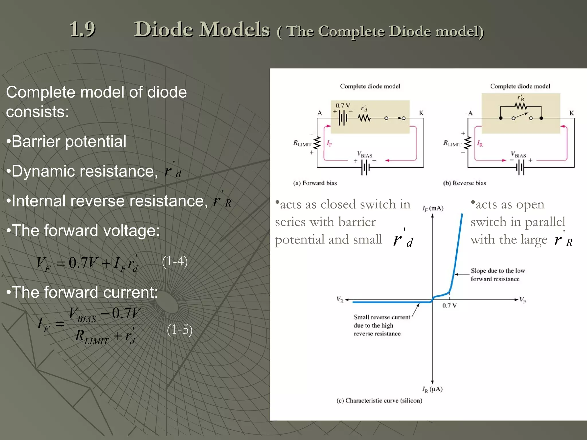
![•Adds the barrier potential to
the ideal switch model
• ‘ is neglected
•From figure (c):
The forward current [by
applying Kirchhoff’s voltage
low to figure (a)]
Ohm’s Law
dr'
•Equivalent to close
switch in series with a
small equivalent voltage
source equal to the barrier
potential 0.7V
•Represent by
produced across the pn
junction
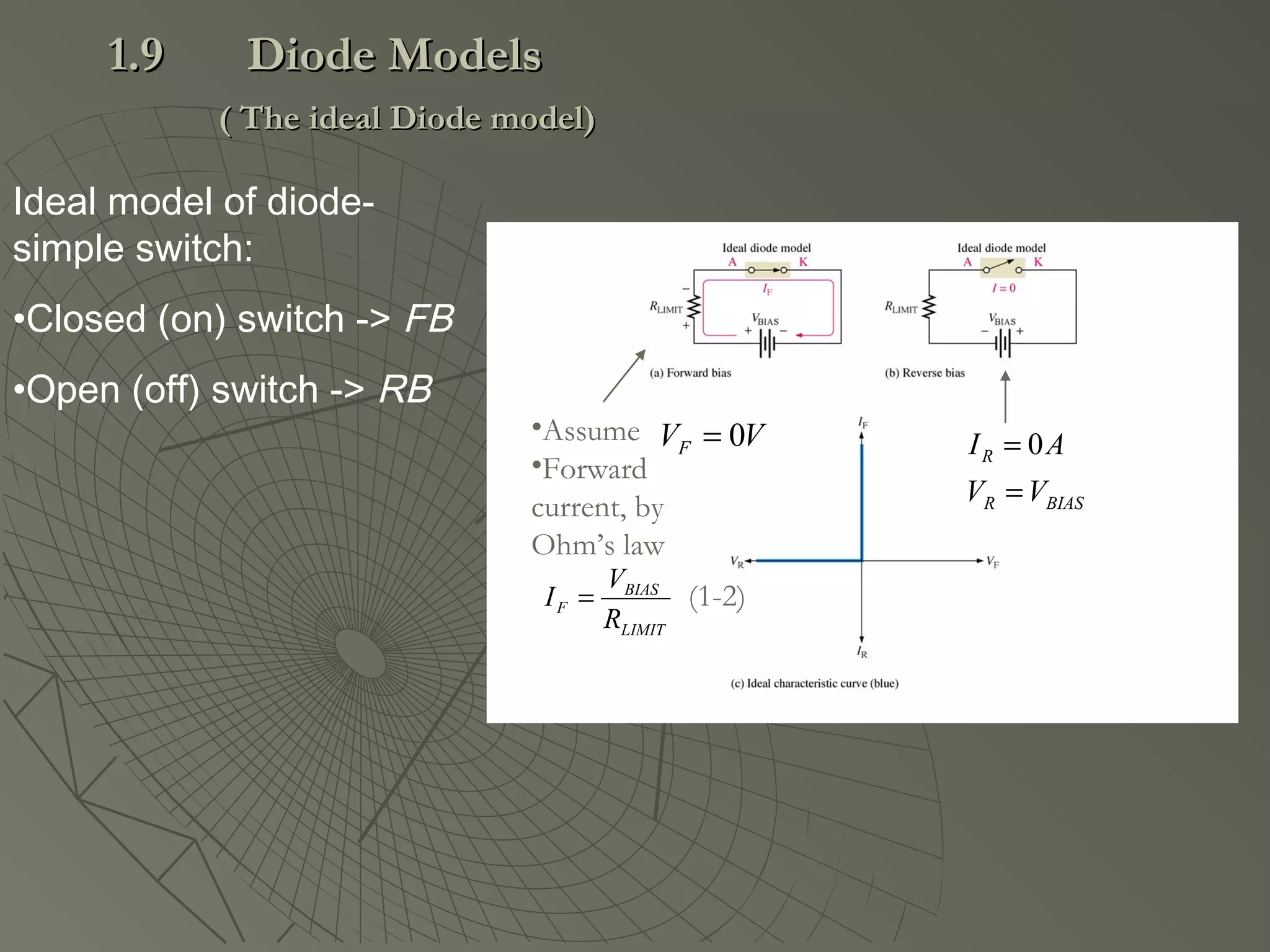
FV
•Same as ideal diode
model
)(3.0
)(7.0
GeVV
SiVV
F
F
=
=
0=−− LIMITRFBIAS VVV
LIMITFR RIV LIMIT
=
LIMIT
FBIAS
F
R
VV
I
−
=
BIASR
R
VV
AI
=
= 0
(1-3)
1.91.9 Diode ModelsDiode Models ( The Practical Diode model)( The Practical Diode model)](https://image.slidesharecdn.com/semiconductorbasics-170507125345/75/Semiconductor-basics-12-2048.jpg)
![10V10V
1.0kΩ1.0kΩ
5V5V
1.0kΩ1.0kΩ
(1) Determine the forward voltage and forward current
[forward bias] for each of the diode model also find the
voltage across the limiting resistor in each cases.
Assumed rd’ = 10Ω at the determined value of forward
current.
1.91.9 Diode ModelsDiode Models ( Example)( Example)](https://image.slidesharecdn.com/semiconductorbasics-170507125345/75/Semiconductor-basics-14-2048.jpg)
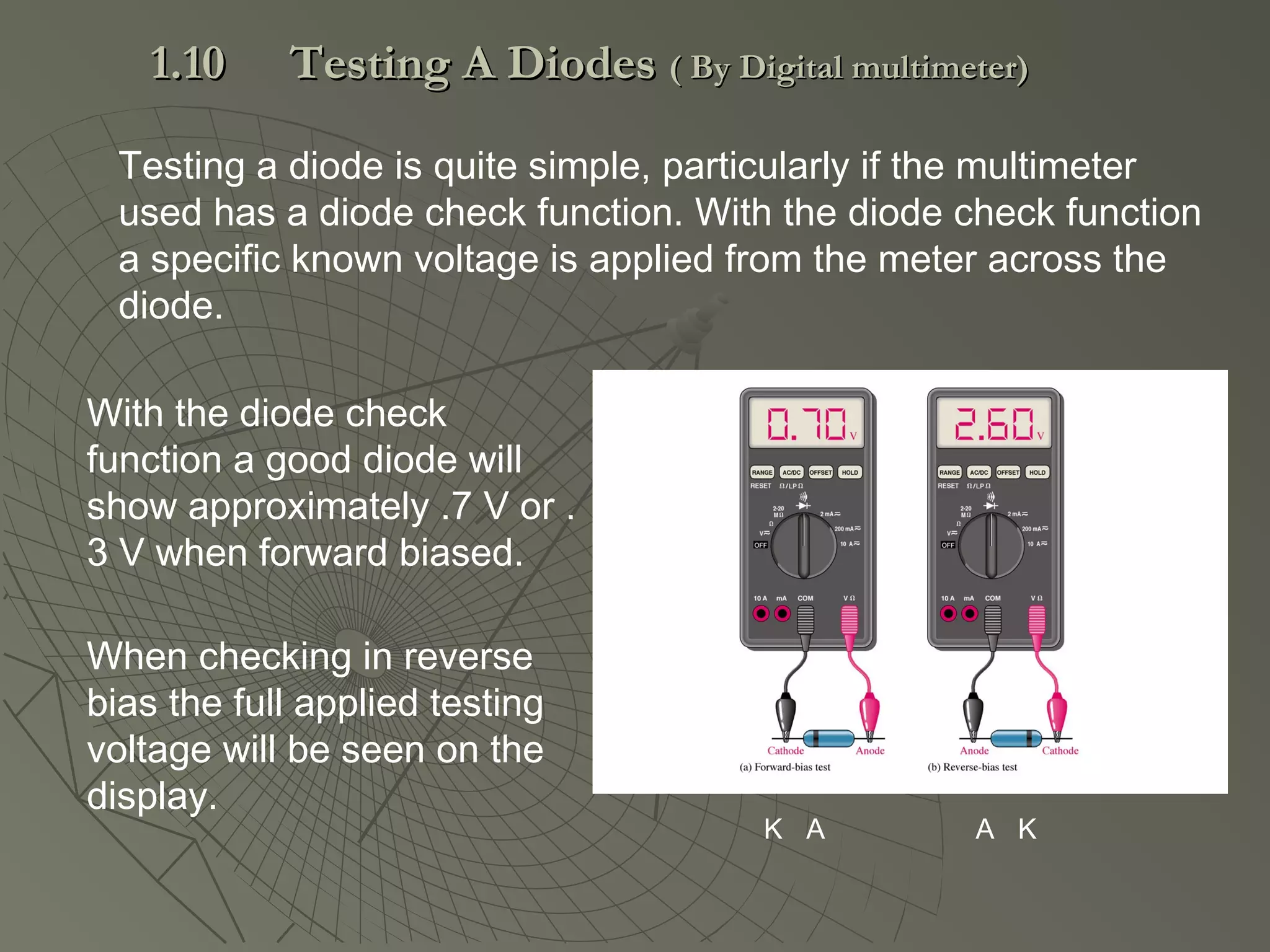
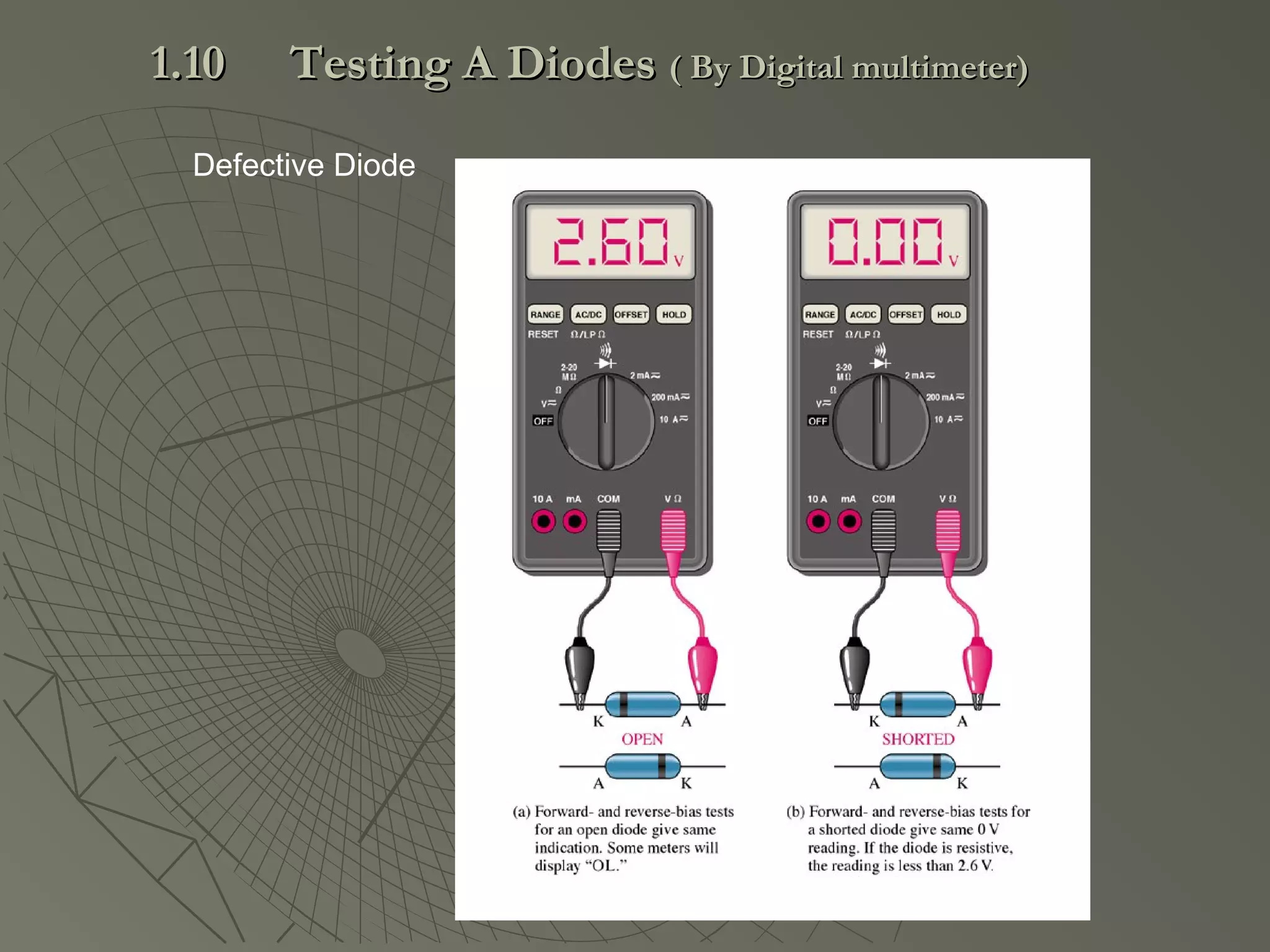

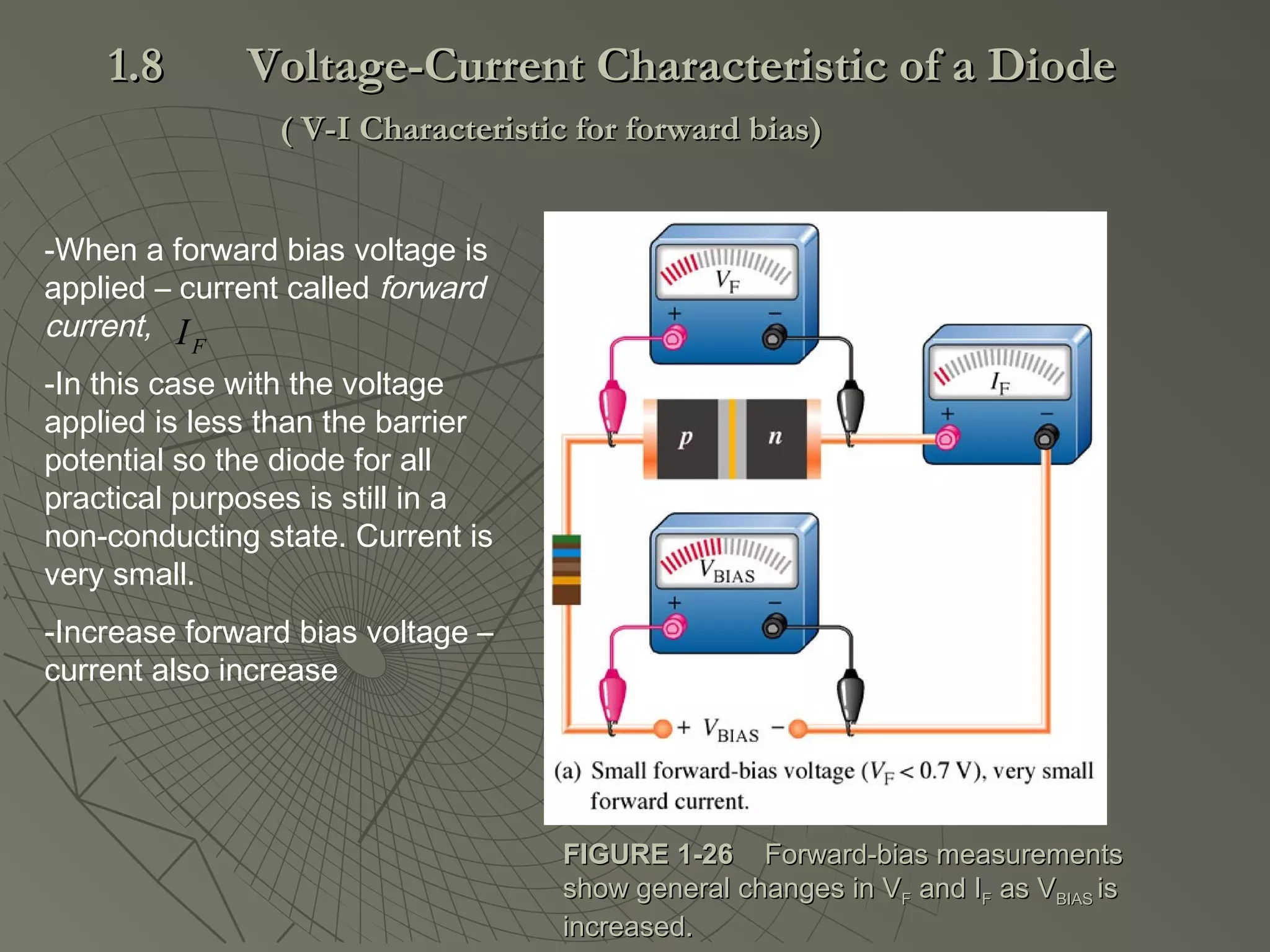
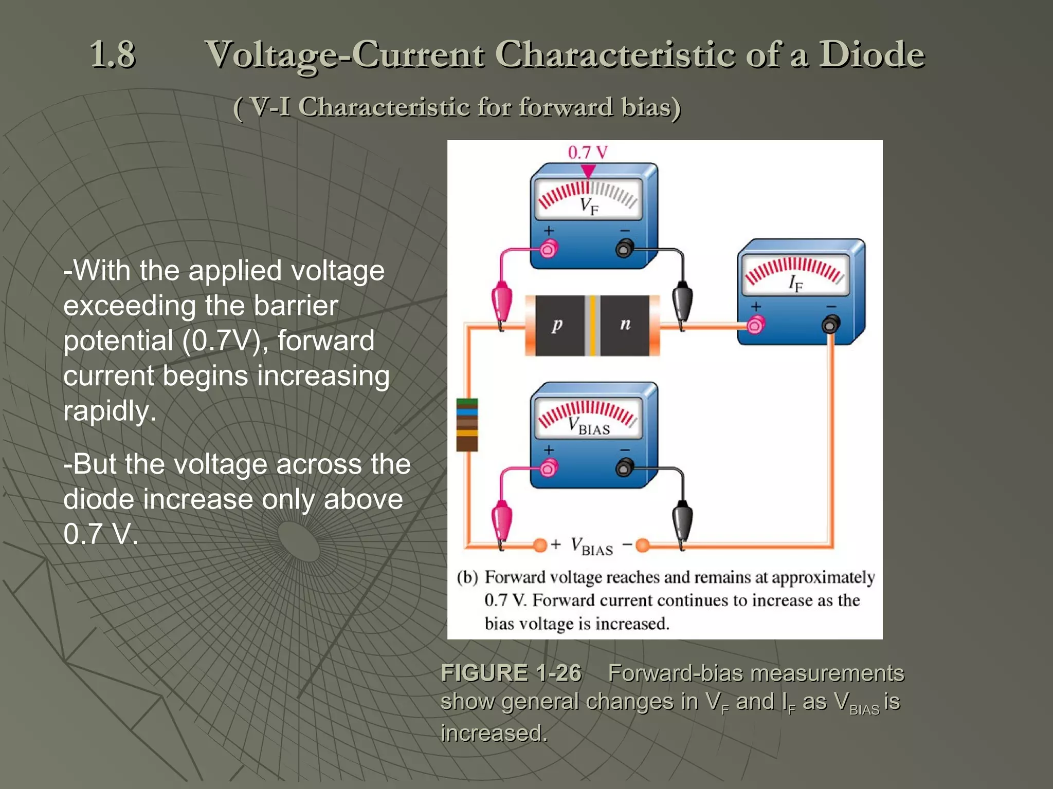
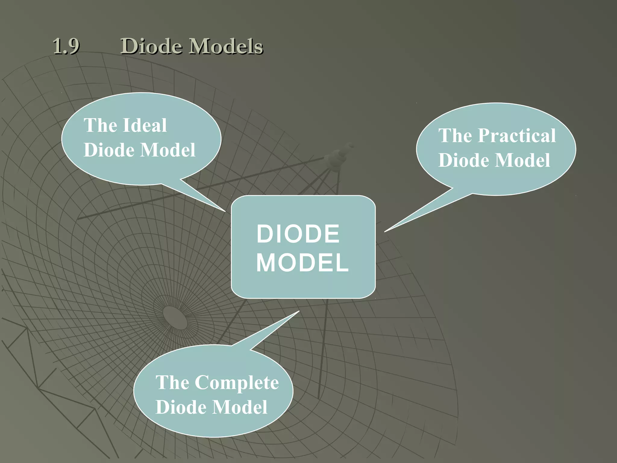
- A diode allows current to flow in only one direction, exhibiting different characteristics and behaviors under forward and reverse bias. When forward biased, current flows easily but requires a minimum voltage of around 0.7V. When reverse biased, very little current flows. - There are three models used to analyze a diode: the ideal model, which assumes it acts as a closed switch under forward bias; the practical model, which adds a barrier potential and small resistance; and the complete model, which also includes a dynamic resistance. - Diodes can be tested using a multimeter to check the forward and reverse bias voltages are around 0.7V and close to the supply voltage respectively. This confirms the diode's functionality and polarity.


