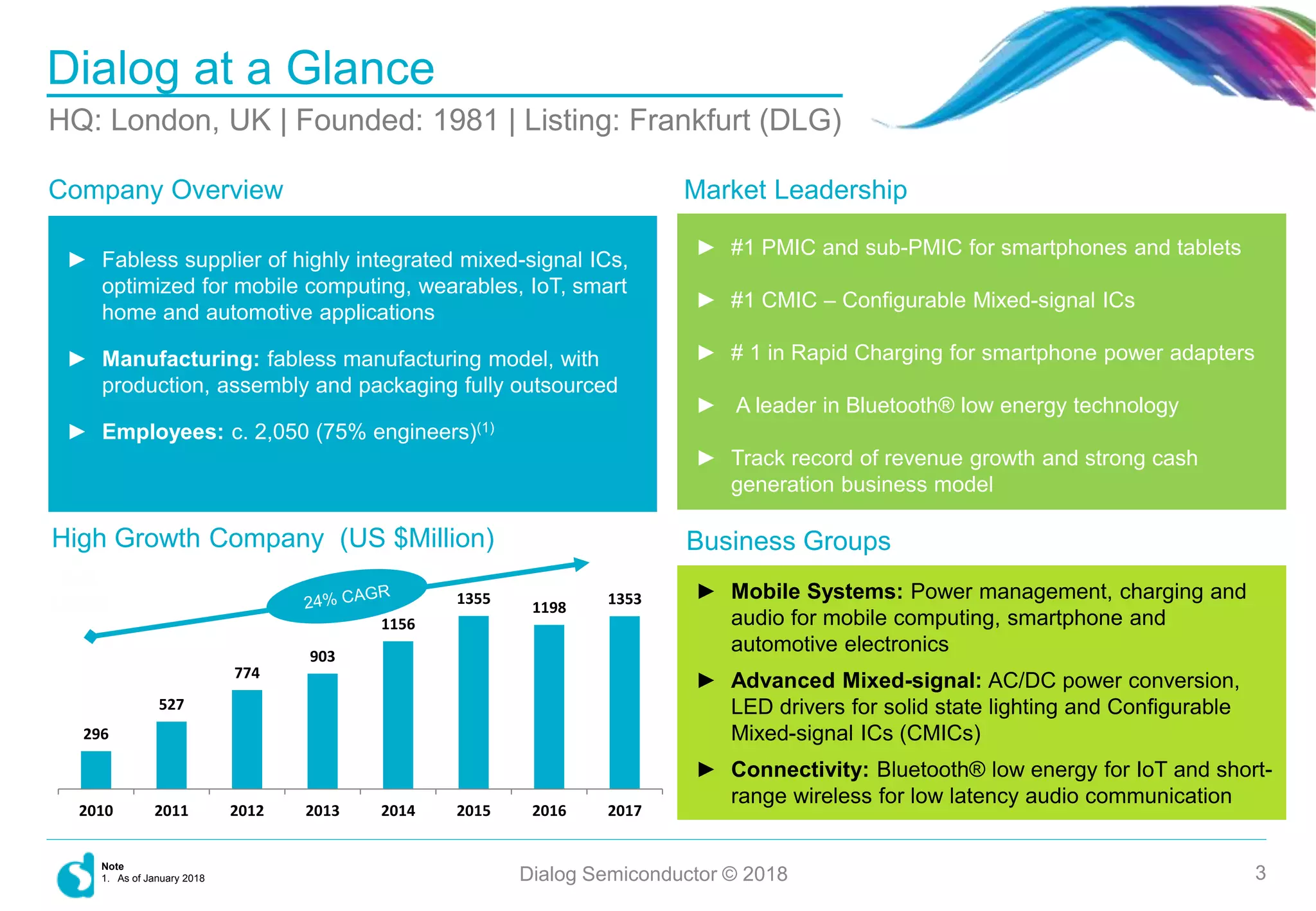
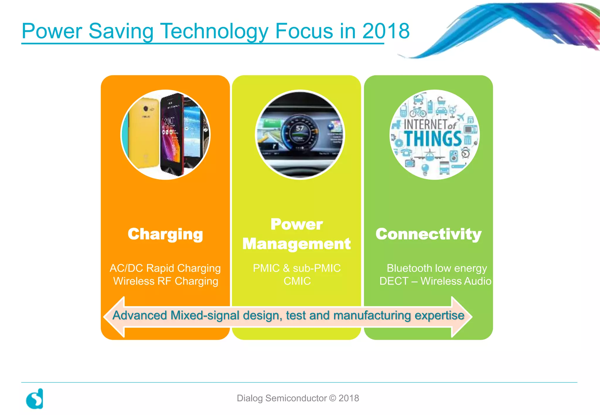
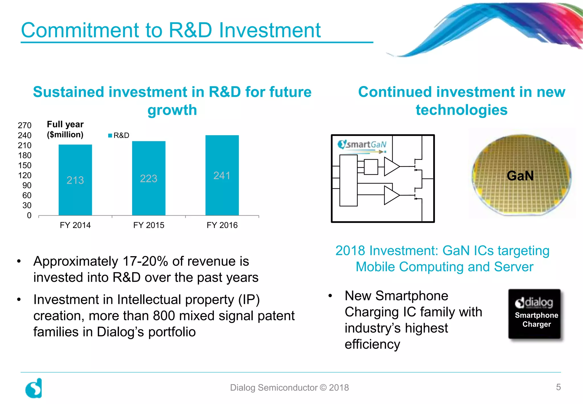
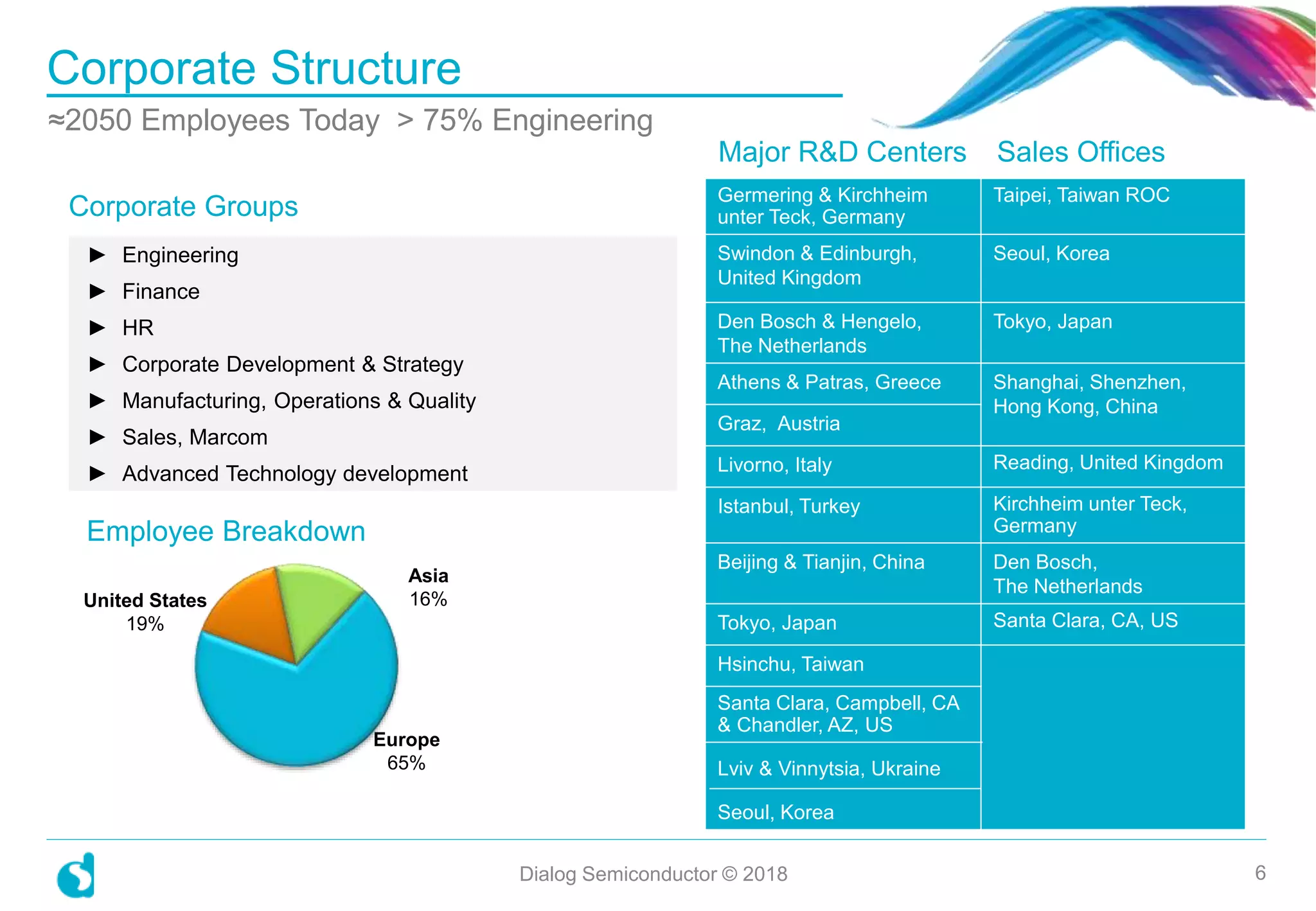
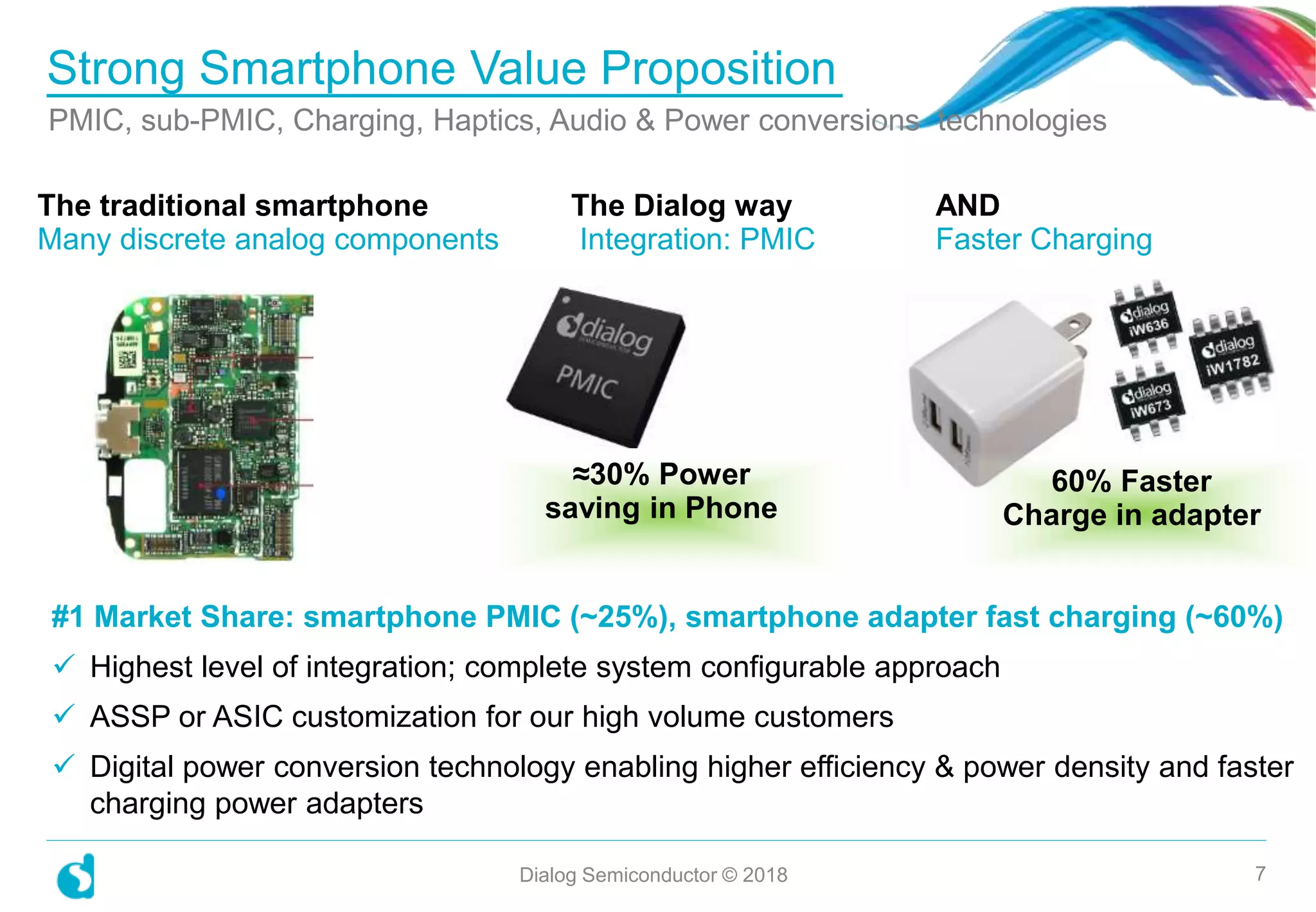
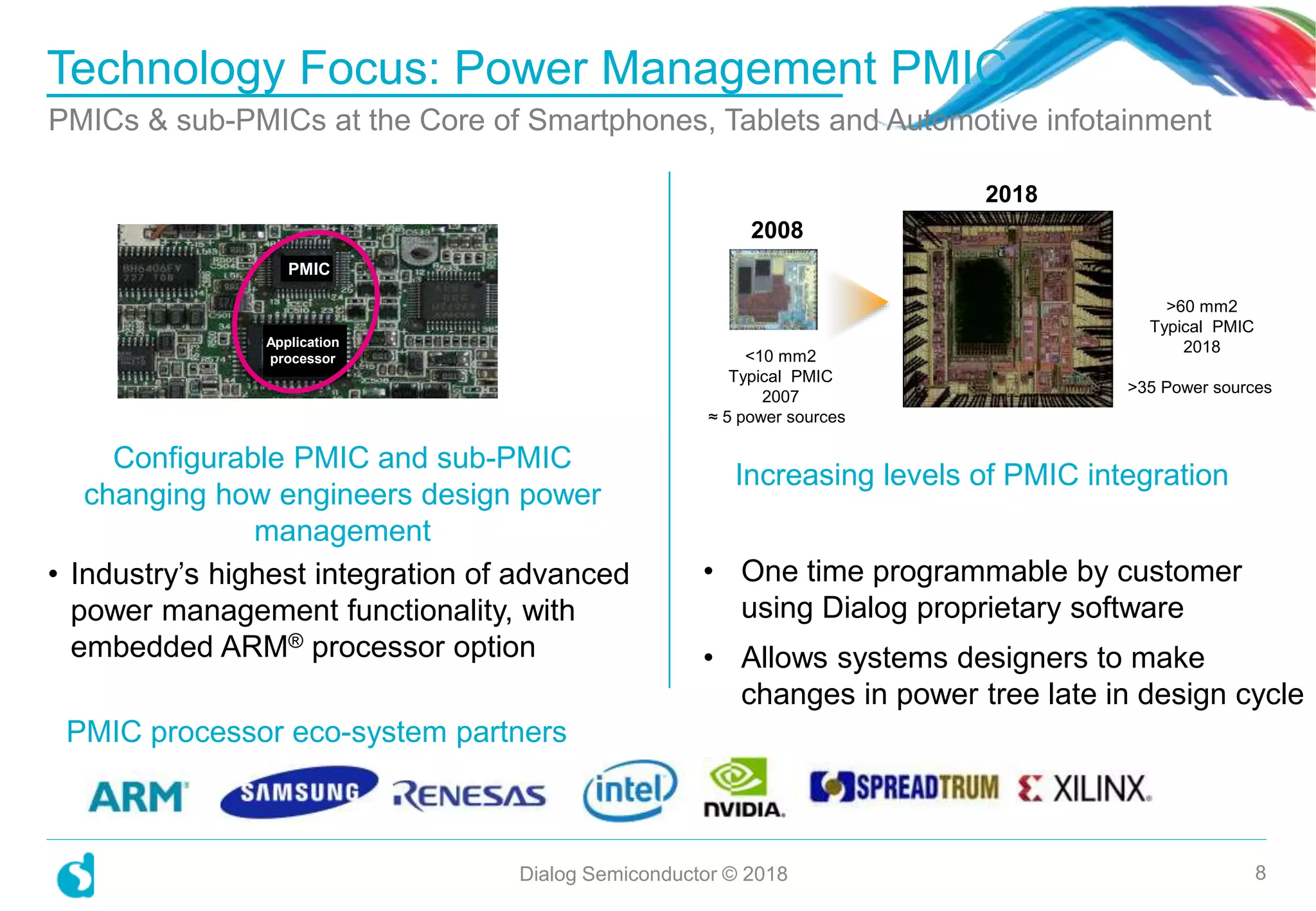
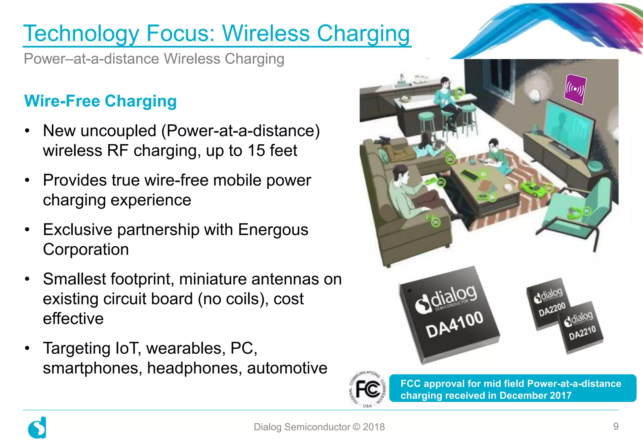
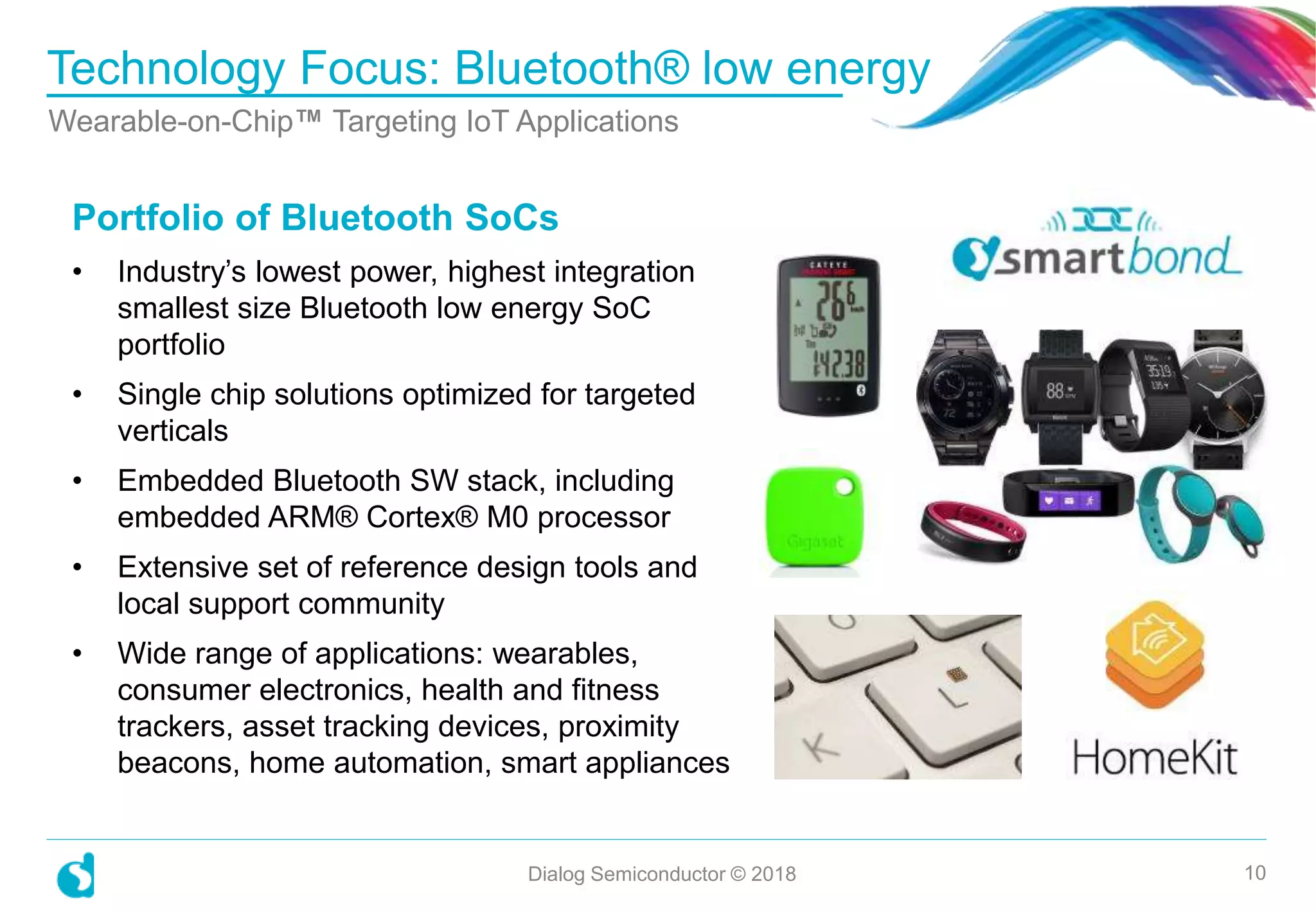
…personal
…portable
…connected
Analog Test Engineering
Politecnico di Torino
Dr Peter Sarson
7th December 2018
Dialog Semiconductor © 2018
Introduction to Dialog Semiconductor
Fundamentals
Test Instrumentation
Accuracy and Resolution
Deep Dive
New Standards
Dialog Semiconductor © 2018 2
Agenda
296
527
774
903
1156
1355
1198
1353
2010 2011 2012 2013 2014 2015 2016 2017
Dialog at a Glance
HQ: London, UK | Founded: 1981 | Listing: Frankfurt (DLG)
Dialog Semiconductor © 2018 3
► Fabless supplier of highly integrated mixed-signal ICs,
optimized for mobile computing, wearables, IoT, smart
home and automotive applications
► Manufacturing: fabless manufacturing model, with
production, assembly and packaging fully outsourced
► Employees: c. 2,050 (75% engineers)(1)
Business Groups
► Mobile Systems: Power management, charging and
audio for mobile computing, smartphone and
automotive electronics
► Advanced Mixed-signal: AC/DC power conversion,
LED drivers for solid state lighting and Configurable
Mixed-signal ICs (CMICs)
► Connectivity: Bluetooth® low energy for IoT and short-
range wireless for low latency audio communication
Company Overview
► #1 PMIC and sub-PMIC for smartphones and tablets
► #1 CMIC – Configurable Mixed-signal ICs
► # 1 in Rapid Charging for smartphone power adapters
► A leader in Bluetooth® low energy technology
► Track record of revenue growth and strong cash
generation business model
High Growth Company (US $Million)
Note
1. As of January 2018
Market Leadership
Power Saving Technology Focus in 2018
Dialog Semiconductor © 2018
4
Charging
Power
Management
Connectivity
Advanced Mixed-signal design, test and manufacturing expertise
PMIC & sub-PMIC
CMIC
Bluetooth low energy
DECT – Wireless Audio
AC/DC Rapid Charging
Wireless RF Charging
Sustained investment in R&D for future
growth
• Approximately 17-20% of revenue is
invested into R&D over the past years
• Investment in Intellectual property (IP)
creation, more than 800 mixed signal patent
families in Dialog’s portfolio
Commitment to R&D Investment
Dialog Semiconductor © 2018 5
• New Smartphone
Charging IC family with
industry’s highest
efficiency
213 223 241
0
30
60
90
120
150
180
210
240
270
FY 2014 FY 2015 FY 2016
R&D
Full year
($million)
Continued investment in new
technologies
GaN
2018 Investment: GaN ICs targeting
Mobile Computing and Server
Smartphone
Charger
Corporate Structure
Dialog Semiconductor © 2018 6
≈2050 Employees Today > 75% Engineering
Employee Breakdown
United States
19%
Asia
16%
Europe
65%
Germering & Kirchheim
unter Teck, Germany
Taipei, Taiwan ROC
Swindon & Edinburgh,
United Kingdom
Seoul, Korea
Den Bosch & Hengelo,
The Netherlands
Tokyo, Japan
Athens & Patras, Greece Shanghai, Shenzhen,
Hong Kong, China
Graz, Austria
Livorno, Italy Reading, United Kingdom
Istanbul, Turkey Kirchheim unter Teck,
Germany
Beijing & Tianjin, China Den Bosch,
The Netherlands
Tokyo, Japan Santa Clara, CA, US
Hsinchu, Taiwan
Santa Clara, Campbell, CA
& Chandler, AZ, US
Lviv & Vinnytsia, Ukraine
Seoul, Korea
► Engineering
► Finance
► HR
► Corporate Development & Strategy
► Manufacturing, Operations & Quality
► Sales, Marcom
► Advanced Technology development
Corporate Groups
Major R&D Centers Sales Offices
#1 Market Share: smartphone PMIC (~25%), smartphone adapter fast charging (~60%)
 Highest level of integration; complete system configurable approach
 ASSP or ASIC customization for our high volume customers
 Digital power conversion technology enabling higher efficiency & power density and faster
charging power adapters
Strong Smartphone Value Proposition
Dialog Semiconductor © 2018 7
The Dialog way AND
Integration: PMIC Faster Charging
The traditional smartphone
Many discrete analog components
≈30% Power
saving in Phone
60% Faster
Charge in adapter
PMIC, sub-PMIC, Charging, Haptics, Audio & Power conversions technologies
• Industry’s highest integration of advanced
power management functionality, with
embedded ARM® processor option
Technology Focus: Power Management PMIC
PMICs & sub-PMICs at the Core of Smartphones, Tablets and Automotive infotainment
Dialog Semiconductor © 2018 8
• One time programmable by customer
using Dialog proprietary software
• Allows systems designers to make
changes in power tree late in design cycle
Configurable PMIC and sub-PMIC
changing how engineers design power
management
Increasing levels of PMIC integration
<10 mm2
Typical PMIC
2007
≈ 5 power sources
>60 mm2
Typical PMIC
2018
>35 Power sources
2008
2018
Application
processor
PMIC
PMIC processor eco-system partners
Technology Focus: Wireless Charging
Power–at-a-distance Wireless Charging
Dialog Semiconductor © 2018 9
Wire-Free Charging
• New uncoupled (Power-at-a-distance)
wireless RF charging, up to 15 feet
• Provides true wire-free mobile power
charging experience
• Exclusive partnership with Energous
Corporation
• Smallest footprint, miniature antennas on
existing circuit board (no coils), cost
effective
• Targeting IoT, wearables, PC,
smartphones, headphones, automotive
FCC approval for mid field Power-at-a-distance
charging received in December 2017
Portfolio of Bluetooth SoCs
• Industry’s lowest power, highest integration
smallest size Bluetooth low energy SoC
portfolio
• Single chip solutions optimized for targeted
verticals
• Embedded Bluetooth SW stack, including
embedded ARM® Cortex® M0 processor
• Extensive set of reference design tools and
local support community
• Wide range of applications: wearables,
consumer electronics, health and fitness
trackers, asset tracking devices, proximity
beacons, home automation, smart appliances
Technology Focus: Bluetooth® low energy
Dialog Semiconductor © 2018 10
Wearable-on-Chip™ Targeting IoT Applications
Introduction to Dialog Semiconductor
Fundamentals
Test Instrumentation
Accuracy and Resolution
Deep Dive
New Standards
Dialog Semiconductor © 2018 11
Agenda
Introduction to Dialog Semiconductor
Ohms Law
Test Instrumentation
Accuracy and Resolution
Deep Dive
New Standards
Dialog Semiconductor © 2018 12
Agenda
Ohms Law
Dialog Semiconductor © 2018 13
Thevenin - Norton equivalent circuits
Dialog Semiconductor © 2018 14
Introduction to Dialog Semiconductor
Discrete Signals
Test Instrumentation
Accuracy and Resolution
Deep Dive
New Standards
Dialog Semiconductor © 2018 15
Agenda
AC Signals
Dialog Semiconductor © 2018 16
Sinewave – Continuous
𝑓 𝑡 = 𝐴 sin 2𝜋𝑓𝑡
-1
-0.8
-0.6
-0.4
-0.2
0
0.2
0.4
0.6
0.8
1
0.1 0.3 0.5 0.7 0.9 1.1 1.3 1.5 1.7 1.9 2.1 2.3 2.5 2.7 2.9 3.1 3.3 3.5 3.7 3.9 4.1 4.3 4.5 4.7 4.9 5.1 5.3 5.5 5.7 5.9 6.1
Series1
𝑓𝑠
𝑓𝑡
=
𝑁
𝑀
Fs = Sampling Frequency
Ft = Tone Frequency we want to
generate
N = Number of points the waveform
will have
M = Number of cycles or Bin Number
Sampling Theorem
Dialog Semiconductor © 2018 17
-1
-0.5
0
0.5
1
0 2 4 6
Series1
𝑑 𝑛𝑇𝑠 = 𝐴 sin 2𝜋𝑓𝑛𝑇𝑠
𝑓𝑠
𝑓𝑡
=
𝑁
𝑀
Fs = Sampling Frequency
Ft = Tone Frequency we want to
generate
N = Number of points the waveform
will have
M = Number of cycles or Bin Number
Sampling Theorem
Dialog Semiconductor © 2018 18
-1
-0.5
0
0.5
1
0 2 4 6
Series1
M = 1, 1 cycle
N = 62
𝑓𝑠
𝑓𝑡
=
𝑁
𝑀
Fs = Sampling Frequency
Ft = Tone Frequency we want to
generate
N = Number of points the waveform
will have
M = Number of cycles or Bin Number
Sampling Theorem
Dialog Semiconductor © 2018 19
-1
-0.5
0
0.5
1
0 2 4 6
Series1
If we want a tone frequency of 1 kHz
Then Fs = 62 kHz
Introduction to Dialog Semiconductor
Digitization
Test Instrumentation
Accuracy and Resolution
Deep Dive
New Standards
Dialog Semiconductor © 2018 20
Agenda
Digitization
Dialog Semiconductor © 2018 21
Nyquist - sampling
𝑓𝑠 = 2𝑓𝑡 - Nyquist Theorem (doesn’t work)
𝑓𝑠 = 4𝑓𝑡 - Quadrature sampling, cos(), sin()
-1
-0.5
0
0.5
1
0.1
0.3
0.5
0.7
0.9
1.1
1.3
1.5
1.7
1.9
2.1
2.3
2.5
2.7
2.9
3.1
3.3
3.5
3.7
3.9
4.1
4.3
4.5
4.7
4.9
5.1
5.3
5.5
5.7
5.9
6.1
Series1
𝑓𝑠
𝑓𝑡
=
𝑁
𝑀
Sampling Theorem
remains unchanged
and must be fulfilled
Why
Dialog Semiconductor © 2018 22
Fs = 2Ft
Best Solution
Dialog Semiconductor © 2018 23
Fs = 4Ft
• By doing quadrature
sampling
• The sampled
components are
either cos() or sin()
as each point is
sampled every 90
degrees.
• This allows very
quick computation
Digitization
Dialog Semiconductor © 2018 24
Nyquist - sampling
Using 𝑓𝑠 = 4𝑓𝑡, we want to measure a 1.22 kHz
𝑓𝑠 = 4.88 𝑘𝐻𝑧 , N = 1220, M = 305
-1
-0.5
0
0.5
1
0.1
0.3
0.5
0.7
0.9
1.1
1.3
1.5
1.7
1.9
2.1
2.3
2.5
2.7
2.9
3.1
3.3
3.5
3.7
3.9
4.1
4.3
4.5
4.7
4.9
5.1
5.3
5.5
5.7
5.9
6.1
Series1
𝑓𝑠
𝑓𝑡
=
𝑁
𝑀
Sampling Theorem
remains unchanged
and must be fulfilled
rms
Peak
Peak
to
Peak
Ff = Fs/N - Fourier Frequency (Frequency Resolution)
Ff = Ft/M - Fourier Frequency (Frequency Resolution)
UTP = 1 / Ff - Unit Test Period – Time to complete the
playout of the waveform
r = 2/N - Phase resolution
Other Stuff
Dialog Semiconductor © 2018 25
The larger the number of points, the higher the resolution
Introduction to Dialog Semiconductor
Fourier Analysis
Test Instrumentation
Accuracy and Resolution
Deep Dive
New Standards
Dialog Semiconductor © 2018 26
Agenda
Fourier Analysis
Dialog Semiconductor © 2018 27
• Spectral Analysis of a signal
• Different types of Analysis
• Magnitude FFT (MagFFT) – Returns the magnitude of each frequency
• Power FFT (PwrFFT) – Returns the magnitude^2 of each frequency
• FFT (FFT) - Returns the cos(), sin() components
• Fourier Volt Meter (FVM) - Returns just the magnitude of one bin
• Description
• MagFFT – Returns an array that’s N/2 in size – slow to execute because of √
• PwrFFT – Returns an array that’s N/2 in size – faster to execute because of no √
• FFT - Returns an N size array containing cos(), sin() components
• FVM - Returns the value of one bin that is supplied by the user. Very fast.
Magnitude FFT Example
Dialog Semiconductor © 2018 28
Introduction to Dialog Semiconductor
Fundamentals
Test Instrumentation
Accuracy and Resolution
Deep Dive
New Standards
Dialog Semiconductor © 2018 29
Agenda
Test Setup
Dialog Semiconductor © 2018 30
• In test we are interested in precision
and accuracy
• Any voltage drop due to cable or trace
resistances needs to be addressed
• On a bench setup, the voltage would
be adjusted until the correct voltage
was observed on the terminals
• For an ATE nothing manual is
possible as we are testing things in
milliseconds.
• Calibration and compensation circuits
are critical to accurate, precise and
repeatable testing
Introduction to Dialog Semiconductor
Fundamentals
What is a tester
Accuracy and Resolution
Deep Dive
New Standards
Dialog Semiconductor © 2018 31
Agenda
YTEC
S50/V50
Pincount 256 I/O
Xcerra
Fusion MX/EX
Teradyne
ETS-88
Tester Platforms Examples
32
Advantest Pinscale/Portscale
High-end PM & Audio IC & RF
High pincount > 1000 I/O
Mixed signal / VI capability
PinCount
Teradyne Ultra Flex
High-end PM & Audio IC
High pincount > 1000 I/O
Teradyne Catalyst
Automotive SoC
Conectivity RF & BB SoC
Pincount < 400 I/O
Teradyne Flex
High-end PM & Audio IC
Pincount < 400 I/O
Teradyne J750/J750EX
Connectivity RF & BB SoC
Pincount > 500 I/O
1000200500
ASL-1000
AC/DC & SSL Product
Pincount < 50 I/O
Credence Quartett/Duo
PM, Audio & Industrial IC
Pincount < 200 I/O
Dialog Semiconductor © 2018
Overview of a Test System
Dialog Semiconductor © 2018 33
Test system components (Integra Flex)
Instrument Architecture
Dialog Semiconductor © 2018 34
Integra Flex
Test Head
Dialog Semiconductor © 2018 35
Loadboard/Probecard
Dialog Semiconductor © 2018 36
Probeheads/Sockets
37Dialog Semiconductor © 2018
Semiconductor Manufacturing Process
How the tester is used
38
Wafer
Loaded into
prober
Wafer
Tested
with
ATE
Good
Test
Program
Tester and wafer prober for WLCSP
Dialog Semiconductor © 2018 39
Tester
Product
Entry
Testhead with
Instruments
Waferprober
Burn-In is the application of thermal and
electrical stress for the purposes of
inducing the failure of "marginal
(microelectronic) devices, those with
inherent defects or defects resulting from
manufacturing aberrations which cause
time and stress dependent failures.
Using a burn in stage can remove these
latent defects
• However, this is very expensive as an
extra test stage is needed
HTOL testing is done at the beginning of a
project to qualify a process and package
Burn In
Dialog Semiconductor © 2018 40
Semiconductor Device Process Flow
Dialog Semiconductor © 2018 41
Automotive and Consumer Flows
Design Fab Assembly
Final
Test
Wafer
Sort
Shipment
Burn
In
Re
Test
Automotive
Flow
Consumer Flow
Introduction to Dialog Semiconductor
Fundamentals
Test Hardware Development
Accuracy and Resolution
Deep Dive
New Standards
Dialog Semiconductor © 2018 42
Agenda
Hardware Development Flow
Introduction to Dialog Semiconductor
Fundamentals
Typical Hardware Issues
Accuracy and Resolution
Deep Dive
New Standards
Dialog Semiconductor © 2018 44
Agenda
Typical Issues
Dialog Semiconductor © 2018 45
 Ground Trace Lengths
 Ground lengths to long, to narrow etc
 Causes larger inductance and
impedance
 Can result in device oscillation
 Solution is only a good check of the
layout
Contact Resistance
Dialog Semiconductor © 2018 46
Introduction to Dialog Semiconductor
Fundamentals
Instrumentation
Accuracy and Resolution
Deep Dive
New Standards
Dialog Semiconductor © 2018 47
Agenda
Introduction to Dialog Semiconductor
Fundamentals
VI
Accuracy and Resolution
Deep Dive
New Standards
Dialog Semiconductor © 2018 48
Agenda
Tester Instruments
Dialog Semiconductor © 2018 49
VI
• Standard Measurement setup capability
• Force Voltage, Measure Current
• Force Current, Measure Voltage
• Accurate Voltage Source with Kelvin Connection
• Force and Sense
• Device protection
• Programmable Voltage and Current clamps
• Four Quadrant operation
• Source and Sink Current
• Force positive and negative voltages
• Possible to stack channels to increase current capability
(Merge Mode)
• Waveform Capture (Digitization) possibilities per pin
• All current measurements are done
using a resistor.
• This measurement is calibrated to a
standard by measuring the voltage
with a set current. Then adjusting
the measured value to the standard
• This offset is then applied to all
measurement using this range.
• Higher currents need lower
resistance to keep the produced
voltage in the same range for
conversion to digital
• Typically a 12-16 bit ADC would be
used for a VI.
Tester Instruments
Dialog Semiconductor © 2018 50
VI
Tester Instruments
Dialog Semiconductor © 2018 51
UVI80 DC-DiffMeter
• High Speed 16 bit or High Precision 24bit
Measurement
• Up To 8MSPS or 100ksps respectively
• Hardware Averaging possible
• UVI80 -Voltage range - ±1,4V, ±3.5V,
±7V
Introduction to Dialog Semiconductor
Fundamentals
Digital
Accuracy and Resolution
Deep Dive
New Standards
Dialog Semiconductor © 2018 52
Agenda
Send or Capture a Digital Response
Dialog Semiconductor © 2018 53
Input signal
Output signal
Vih
Vil
Vol
Voh
Test Period
Strobe Points
Interaction ATE HW - Test Program
Dialog Semiconductor © 2018 54
Comparator
levels – vol,
voh
Interaction ATE HW - Test Program
Dialog Semiconductor © 2018 55
Pattern
comparison
loaded into
memory
Interaction ATE HW - Test Program
Dialog Semiconductor © 2018 56
Compared
on the pin
defined
Interaction ATE HW - Test Program
Dialog Semiconductor © 2018 57
Timing
definition for
each pin
$tset,SCLK,SDATA,ADDR2,RESET_L,
ADDR0,ADDR1,GPIO1,GPIO2,GPIO3,
GPIO4,GPIO5)
> t0_spmi 1 0 0 0 0 0 X X X X X;
> t0_spmi 0 0 0 0 0 0 X X X X X;
> t0_spmi 0 1 0 0 0 0 X X X X X;
> t0_spmi 0 0 0 0 0 0 X X X X X;
> t0_spmi 1 1 0 0 0 0 H H H L L;
> t0_spmi 1 1 0 0 0 0 L L L H L;
> t0_spmi 1 1 0 0 0 0 H L H L H;
> t0_spmi 1 1 0 0 0 0 L H L L H;
> t0_spmi 1 0 0 0 0 0 L L L L L;
Pattern
Dialog Semiconductor © 2018 58
Interpreting a Digital Response
Dialog Semiconductor © 2018 59
Depends
Interpreting a Digital Response
Dialog Semiconductor © 2018 60
Or
Interpreting a Digital Response
Dialog Semiconductor © 2018 61
DSSC
Interpreting a Digital Response
Dialog Semiconductor © 2018 62
DSSC
1
Introduction to Dialog Semiconductor
Fundamentals
Arbitrary Waveform Generator
Accuracy and Resolution
Deep Dive
New Standards
Dialog Semiconductor © 2018 63
Agenda
AWG – Signal Source
Dialog Semiconductor © 2018 64
DAC – Digital to Analog Converter
Where the
digital
waveform is
loaded.
Digital to
Analog
conversion
Output
Analog
Waveform
Several Types exist within ATE
High Resolution – Low Speed (24bits, 100 kHz) – Used for high precision DC signals,
usually has a kelvin connection like on a VI
High Speed - Lower Resolution (16 bits, 250 MHz) – Can be used for modulation signal of
RF devices, (OFDM, QPSK, Chirp, Multitones etc), Baseband signals.
AWG
Dialog Semiconductor © 2018 65
Introduction to Dialog Semiconductor
Fundamentals
Digitizer
Accuracy and Resolution
Deep Dive
New Standards
Dialog Semiconductor © 2018 66
Agenda
Digitizer – Signal Capture
Dialog Semiconductor © 2018 67
ADC –Analog to Digital Converter
Usually a few selectable
LPF to condition the
signal before
conversion
Analog to
Digital
Conversion
Conversion loaded
into DSP so that it
can be readback
and manipulated by
the test engineer
Introduction to Dialog Semiconductor
Fundamentals
Test Setup Examples
Accuracy and Resolution
Deep Dive
New Standards
Dialog Semiconductor © 2018 68
Agenda
Consider the following device pinout
1 VDD
1 GND
3 IO
1 BandGap
1 Voltage Reference
Equates to
3 UVI80
3 HSD1600
Test Efficiency - Example
Dialog Semiconductor © 2018 69
Use the full tester capability at once
With a tester configuration as follows
640 UVI80
512 HSD1600
Therefore we could possibly have a
512/3 = 170 sites
Which would probably be
20*8 = 160 sites
Test Efficiency - Example
Dialog Semiconductor © 2018 70
Use the full tester capability at once
Consider the following device pinout
10 VDD
1 GND
32 IO
22 Voltage Reference
Equates to
32 UVI80
32 HSD1600
Test Efficiency - Example
Dialog Semiconductor © 2018 71
Use the full tester capability at once
With a tester configuration as follows
640 UVI80
512 HSD1600
Therefore we could possibly have a
512/32 = 16 sites
Test Efficiency - Example
Dialog Semiconductor © 2018 72
Use the full tester capability at once
Introduction to Dialog Semiconductor
Fundamentals
Accuracy and Resolution
Deep Dive
New Standards
Dialog Semiconductor © 2018 73
Agenda
Test Instrumentation
Instrument Accuracy and Precision
Dialog Semiconductor © 2018 74
Accuracy
• Accuracy of the instrument is the difference (error)
between the real value and the attained value, either
measured or sourced.
• This is usually quoted as a percentage error of the
range of the instrument used to make the
measurement.
• Teradyne UVI80 ±20uA accuracy is 0.1% + 25 nA
• Teradyne DC30 ±200uA accuracy is 0.1% + 200 nA
• Therefore, if we measure a value of 1uA on the
20uA range, the best measurement than can be
quoted is
• 1uA + 0.01*20uA + 25nA = 1.225uA
• If the 200uA range is used we see
• 1uA + 0.01*200uA + 200nA = 3.20uA
Measured the Noise of
the Instrument
Instrument Accuracy and Precision
Dialog Semiconductor © 2018 75
Resolution
• Resolution of the instrument is to what precision the
target value can attained, either measured or sourced.
• This is usually quoted as a converter resolution, in
bits. This is quoted over a certain range.
• Teradyne UVI80 ±20uA 16 bit resolution ~ 763 pA
• 2^16 = 65536
• 40uA/65536 = 610 pA ? = ENOB 15.7 bits
• So measuring 1uA on 20uA range we can expect
to measure
• 1.225 uA accuracy + 763 pA resolution
• If we increase the current to 1.05uA then the
instrument should see the change because the
resolution is high but the result could be 1.275uA
Instrument Accuracy and Precision
Dialog Semiconductor © 2018 76
Concept
• We can think about this in the following way
8cm
Accuracy
offset
Measurement
precision or
resolution
• The accuracy is how close you get your
ruler to the point you want to measure
from. If you are off by 1cm then the
accuracy is 1cm.
• The resolution is the number of marks
that are on the ruler, if there are spaces
every 1mm then the resolution is 1mm.
The below example 8.5cm would be
measured as 8.0cm.
• It is possible to improve the accuracy
but not the resolution.
• By comparing the measurement to
KNOWN value, the measurement
can be offset, this is called a focus
calibration.
Focus Calibration
Dialog Semiconductor © 2018 77
How to improve accuracy
8cm
By compensating the offset
the accuracy has been
improved but the resolution
of measurement remains
unchanged.
• For instance, if there is an open circuit,
we know there should be no current
flowing. So if a current measurement is
made under these conditions, the
measured current can be subtracted
from a real measurement to
compensate for the offset.
Introduction to Dialog Semiconductor
Fundamentals
Test Instrumentation
Accuracy and Resolution
Deep Dive
New Standards
Dialog Semiconductor © 2018 78
Agenda
Introduction to Dialog Semiconductor
Fundamentals
Test Instrumentation
Accuracy and Resolution
What are Defects, and how are they seen
New Standards
Dialog Semiconductor © 2018 79
Agenda
A defect has been defined as :-
• an unintended change in a circuit’s
physical implementation
– the circuit might or might not meet its
specifications
– In an analogue circuit, a short circuit or
an excessive narrowing of a resistor
might cause gain to decrease by a few
percent
A defect can be seen as
• A catastrophic fail – complete failure
• Marginal failure – device fails just out
side of limits
• A functional failure only seen at
positive or negative temperature
What is a defect and how are they seen?
Dialog Semiconductor © 2018 80
Device
Failures
Latent defect
• A defect that cannot be seen easily seen at normal testing which will fail after
some hours of operations – Also known as early life time failures
What is a defect and how are they seen?
Dialog Semiconductor © 2018 81
Manufacturing defects
Dialog Semiconductor © 2018 82
• A defect is a physical flaw introduced into the circuit during the manufacturing process.
• It is any deviation from the intended specification.
• A defect will change the behavior of the circuit,
but may not be detectable.
• A defect may cause a circuit failure, it may
present a future reliability risk, or it may
never cause a problem.
– Doping Errors
• Concentrations of charge in material
– DC offsets
– Distortions
– Noise
– Under-etching
• No connects at Vias
– Misalignment
• Incorrect or no connects
– Incomplete Etch
• Areas of incomplete etching
– Blocked Etch
• Particle interference
Other Defects Types
Dialog Semiconductor © 2018 83
Manufacturing defects
84
Cut direction
Thin oxide barrier
Dialog Semiconductor © 2018
Semiconductor Test Engineering
Dialog Semiconductor © 2018 85
Fault Models
• Using Fault models a test program
can be efficiently designed
– Its important not to produce a test
program that not only detects good
units but forcibly puts devices in a
stress condition such that any bad parts
show themselves clear and are not
marginal good
Doing a TFMEA (Test Failure Mode Effects
Analysis ) will help to analyse how faults in
circuits will show themselves in form of a
output response
• Analysing the potential responses to
the fault will determine if that fault is
screenable
Introduction to Dialog Semiconductor
Fundamentals
Test Instrumentation
Accuracy and Resolution
The Effects of Low Voltage screening
New Standards
Dialog Semiconductor © 2018 86
Agenda
The effects of low voltage screening
Dialog Semiconductor © 2018 87
Effect of low temperature on silicon
decreases the speed of the silicon i.e.
increases the effect of resistance
• By lowering the voltage of the device
compared to normal operation
simulates low temperature testing
When done properly, this technique allows
the screening of defects that can only be
seen at negative temperature
– Hence, saves a temperature
screening stage
– Saves cost $$$$, increases quality of
product delivered to the customer.
• Implemented in all test
programs by Automotive
suppliers.
The effects of low voltage screening
Device failure at -40 degrees at 2.2V
Dialog Semiconductor © 2018 88
Reference :- Peter Sarson, “Very low supply voltage room temperature test to screen low
temperature soft blown fuse fails which result in a resistive bridge”, 2016 17th
International Symposium on Quality Electronic Design (ISQED) Pages: 135 - 139
The effects of low voltage screening
Device functional at 1.825V – 2.2V @ 35 degrees
Dialog Semiconductor © 2018 89
Reference :- Peter Sarson, “Very low supply voltage room temperature test to screen low
temperature soft blown fuse fails which result in a resistive bridge”, 2016 17th
International Symposium on Quality Electronic Design (ISQED) Pages: 135 - 139
The effects of low voltage screening
Device functional at 1.825V – 2.2V @ 35 degrees
Dialog Semiconductor © 2018 90
Reference :- Peter Sarson, “Very low supply voltage room temperature test to screen low
temperature soft blown fuse fails which result in a resistive bridge”, 2016 17th
International Symposium on Quality Electronic Design (ISQED) Pages: 135 - 139
The effects of low voltage screening
Wafermap of -40 degrees screening at 2.2V – Bad Wafer
Dialog Semiconductor © 2018 91
Reference :- Peter Sarson, “Very low supply voltage room temperature test to screen low
temperature soft blown fuse fails which result in a resistive bridge”, 2016 17th
International Symposium on Quality Electronic Design (ISQED) Pages: 135 - 139
The effects of low voltage screening
Correlation wafermap screening at 1.8V @ 35 degrees – Bad
wafer
Dialog Semiconductor © 2018 92
Reference :- Peter Sarson, “Very low supply voltage room temperature test to screen low
temperature soft blown fuse fails which result in a resistive bridge”, 2016 17th
International Symposium on Quality Electronic Design (ISQED) Pages: 135 - 139
The effects of low voltage screening
Stack map of 30 lots – 4.6 Million dies, 3ppm failure rate
Dialog Semiconductor © 2018 93
Reference :- Peter Sarson, “Very low supply voltage room temperature test to screen low
temperature soft blown fuse fails which result in a resistive bridge”, 2016 17th
International Symposium on Quality Electronic Design (ISQED) Pages: 135 - 139
Introduction to Dialog Semiconductor
Fundamentals
Test Instrumentation
Accuracy and Resolution
The Effects of High Voltage Stress
New Standards
Dialog Semiconductor © 2018 94
Agenda
Semiconductor Lifetime
Dialog Semiconductor © 2018 95
Referring to the bathtub curve we have 3
area
• Early Lifetime failure
• Normal operating region
• End of Life – Wearout
The biggest issue for semiconductor
manufactures is Early Life Time Failures
especially automotive suppliers.
• The lower the defect density of the fab,
the lower this reject rate will be,
however, it is the aim of all
semiconductor manufactures to reduce
this as low as possible
Semiconductor Lifetime
Dialog Semiconductor © 2018 96
Gate Oxide
• Ideally , High Ohmic
• Latent defect has lower ohmic value
• will eventually become short
Time from latent defect to short
(catastrophic defect)
• Dependent on voltage and
temperature
Gate Oxide
Dialog Semiconductor © 2018 97
Thin oxide caused device to
breakdown and fail
Device aging can also be carried out by
voltage stress
• This entails exceeding the maximum
rating of a device by a short time period
• To screen oxide failures we need to
stress
– The gate of a transistor
– Between the power and ground of a
transistor
– And measure the current in different
states of the device
– This require two different stress
conditions
Burn-in Simulation
Dialog Semiconductor © 2018 98
• pinA pinB pinC
• 1 1 1
• 1 1 1
• 1 0 0 stop stress meas
• 1 0 0
• 1 1 1
• 0 0 0 stop stress meas
• 1 1 1
• 0 1 0
• 1 1 1 stop stress meas
Dynamic Stress
VDDstress = 1.3xVDDmax – IDDq scan pattern run
Dialog Semiconductor © 2018 99
Reference :- M. Quach; Tuan Pham; T. Figal; B. Kopitzke; P. O'Neill, “ Wafer-level
defect-based testing using enhanced voltage stress and statistical test data
evaluation”, Test Conference, 2002. Proceedings. International
Static Stress
VDDstress = 1.8xVDDmax - IDDq scan pattern run
Dialog Semiconductor © 2018 100
Reference :- M. Quach; Tuan Pham; T. Figal; B. Kopitzke; P. O'Neill, “ Wafer-level defect-
based testing using enhanced voltage stress and statistical test data evaluation”, Test
Conference, 2002. Proceedings. International
Iddq Delta data
Dialog Semiconductor © 2018 101
Effect of Stress voltage over time on leakage current
Time
Increasing leakage
current due to increasing
breakdown of oxide due
to over voltage stress.
By doing this study the process is
understood.
• A high voltage stress can be applied
thus
– A normal circuit will see no changes in
circuit behaviour
– A thin oxide however will degrade
rapidly and a potential latent defect will
have been forcibly discovered and can
removed.
• Thus removing a potential Early Life
Time Failure
How does this help in Production?
Dialog Semiconductor © 2018 102
Removes latent defects
• Therefore decreases the dppm (
defects parts per million)
• Happy customer
Introduction to Dialog Semiconductor
Fundamentals
Test Instrumentation
Accuracy and Resolution
Deep Dive
New Standards
Dialog Semiconductor © 2018 103
Agenda
Introduction to Dialog Semiconductor
Fundamentals
Test Instrumentation
Accuracy and Resolution
Deep Dive
1687.2
Dialog Semiconductor © 2018 104
Agenda
Standardized Analog Test Access
1687.2
Dialog Semiconductor © 2018 105
Standardized description of systematic analog DFT
• 1687 ICL + analog extensions to describe widely-used MS DFT
techniques
• Can describe test access paths, instruments capabilities, and
port characteristics
• Simplifies block-level DFT + fault simulation, and supports
automated chip-level DFT
Standardized description of efficient analog tests
• 1687 PDL + analog extensions for measurements, limits,
instrument requirements, sequence
• Simplifies block-level test generation and automated re-use at
IC-level or in other ICs
• Facilitates generation of optimal tests for efficient simulation and
reliable transfer to ATE
Introduction to Dialog Semiconductor
Fundamentals
Test Instrumentation
Accuracy and Resolution
Deep Dive
2427
Dialog Semiconductor © 2018 106
Agenda
Standardized Analog Fault Models
2427
Dialog Semiconductor © 2018 107
• The purpose of this standard is to enable the calculation of defect
coverage of an Analog Circuit
• Facilitates the assessment of the testability of a circuit
• Potential for predicting test times and possible test escapes
• Using comparisons of DFT & test techniques, this standard
has the possibility to drive automation and quality
improvements.
• Summary of Potential Benefits
• Definition of defect universe for a given analog circuit
• Standard Test Coverage Metrics for A/MS circuits
• Reduction of test times without loss of test coverage
• A more deterministic way to estimate dppm for analog circuits
…personal
…portable
…connected
…personal
…portable
…connected
Dialog Semiconductor © 2018 108
Powering the Smart
Connected Future
www.dialog-semiconductor.com

Politecnico di Torino Test Engineering Lecture

  • 1.
    …personal …portable …connected Analog Test Engineering Politecnicodi Torino Dr Peter Sarson 7th December 2018 Dialog Semiconductor © 2018
  • 2.
    Introduction to DialogSemiconductor Fundamentals Test Instrumentation Accuracy and Resolution Deep Dive New Standards Dialog Semiconductor © 2018 2 Agenda
  • 3.
    296 527 774 903 1156 1355 1198 1353 2010 2011 20122013 2014 2015 2016 2017 Dialog at a Glance HQ: London, UK | Founded: 1981 | Listing: Frankfurt (DLG) Dialog Semiconductor © 2018 3 ► Fabless supplier of highly integrated mixed-signal ICs, optimized for mobile computing, wearables, IoT, smart home and automotive applications ► Manufacturing: fabless manufacturing model, with production, assembly and packaging fully outsourced ► Employees: c. 2,050 (75% engineers)(1) Business Groups ► Mobile Systems: Power management, charging and audio for mobile computing, smartphone and automotive electronics ► Advanced Mixed-signal: AC/DC power conversion, LED drivers for solid state lighting and Configurable Mixed-signal ICs (CMICs) ► Connectivity: Bluetooth® low energy for IoT and short- range wireless for low latency audio communication Company Overview ► #1 PMIC and sub-PMIC for smartphones and tablets ► #1 CMIC – Configurable Mixed-signal ICs ► # 1 in Rapid Charging for smartphone power adapters ► A leader in Bluetooth® low energy technology ► Track record of revenue growth and strong cash generation business model High Growth Company (US $Million) Note 1. As of January 2018 Market Leadership
  • 4.
    Power Saving TechnologyFocus in 2018 Dialog Semiconductor © 2018 4 Charging Power Management Connectivity Advanced Mixed-signal design, test and manufacturing expertise PMIC & sub-PMIC CMIC Bluetooth low energy DECT – Wireless Audio AC/DC Rapid Charging Wireless RF Charging
  • 5.
    Sustained investment inR&D for future growth • Approximately 17-20% of revenue is invested into R&D over the past years • Investment in Intellectual property (IP) creation, more than 800 mixed signal patent families in Dialog’s portfolio Commitment to R&D Investment Dialog Semiconductor © 2018 5 • New Smartphone Charging IC family with industry’s highest efficiency 213 223 241 0 30 60 90 120 150 180 210 240 270 FY 2014 FY 2015 FY 2016 R&D Full year ($million) Continued investment in new technologies GaN 2018 Investment: GaN ICs targeting Mobile Computing and Server Smartphone Charger
  • 6.
    Corporate Structure Dialog Semiconductor© 2018 6 ≈2050 Employees Today > 75% Engineering Employee Breakdown United States 19% Asia 16% Europe 65% Germering & Kirchheim unter Teck, Germany Taipei, Taiwan ROC Swindon & Edinburgh, United Kingdom Seoul, Korea Den Bosch & Hengelo, The Netherlands Tokyo, Japan Athens & Patras, Greece Shanghai, Shenzhen, Hong Kong, China Graz, Austria Livorno, Italy Reading, United Kingdom Istanbul, Turkey Kirchheim unter Teck, Germany Beijing & Tianjin, China Den Bosch, The Netherlands Tokyo, Japan Santa Clara, CA, US Hsinchu, Taiwan Santa Clara, Campbell, CA & Chandler, AZ, US Lviv & Vinnytsia, Ukraine Seoul, Korea ► Engineering ► Finance ► HR ► Corporate Development & Strategy ► Manufacturing, Operations & Quality ► Sales, Marcom ► Advanced Technology development Corporate Groups Major R&D Centers Sales Offices
  • 7.
    #1 Market Share:smartphone PMIC (~25%), smartphone adapter fast charging (~60%)  Highest level of integration; complete system configurable approach  ASSP or ASIC customization for our high volume customers  Digital power conversion technology enabling higher efficiency & power density and faster charging power adapters Strong Smartphone Value Proposition Dialog Semiconductor © 2018 7 The Dialog way AND Integration: PMIC Faster Charging The traditional smartphone Many discrete analog components ≈30% Power saving in Phone 60% Faster Charge in adapter PMIC, sub-PMIC, Charging, Haptics, Audio & Power conversions technologies
  • 8.
    • Industry’s highestintegration of advanced power management functionality, with embedded ARM® processor option Technology Focus: Power Management PMIC PMICs & sub-PMICs at the Core of Smartphones, Tablets and Automotive infotainment Dialog Semiconductor © 2018 8 • One time programmable by customer using Dialog proprietary software • Allows systems designers to make changes in power tree late in design cycle Configurable PMIC and sub-PMIC changing how engineers design power management Increasing levels of PMIC integration <10 mm2 Typical PMIC 2007 ≈ 5 power sources >60 mm2 Typical PMIC 2018 >35 Power sources 2008 2018 Application processor PMIC PMIC processor eco-system partners
  • 9.
    Technology Focus: WirelessCharging Power–at-a-distance Wireless Charging Dialog Semiconductor © 2018 9 Wire-Free Charging • New uncoupled (Power-at-a-distance) wireless RF charging, up to 15 feet • Provides true wire-free mobile power charging experience • Exclusive partnership with Energous Corporation • Smallest footprint, miniature antennas on existing circuit board (no coils), cost effective • Targeting IoT, wearables, PC, smartphones, headphones, automotive FCC approval for mid field Power-at-a-distance charging received in December 2017
  • 10.
    Portfolio of BluetoothSoCs • Industry’s lowest power, highest integration smallest size Bluetooth low energy SoC portfolio • Single chip solutions optimized for targeted verticals • Embedded Bluetooth SW stack, including embedded ARM® Cortex® M0 processor • Extensive set of reference design tools and local support community • Wide range of applications: wearables, consumer electronics, health and fitness trackers, asset tracking devices, proximity beacons, home automation, smart appliances Technology Focus: Bluetooth® low energy Dialog Semiconductor © 2018 10 Wearable-on-Chip™ Targeting IoT Applications
  • 11.
    Introduction to DialogSemiconductor Fundamentals Test Instrumentation Accuracy and Resolution Deep Dive New Standards Dialog Semiconductor © 2018 11 Agenda
  • 12.
    Introduction to DialogSemiconductor Ohms Law Test Instrumentation Accuracy and Resolution Deep Dive New Standards Dialog Semiconductor © 2018 12 Agenda
  • 13.
  • 14.
    Thevenin - Nortonequivalent circuits Dialog Semiconductor © 2018 14
  • 15.
    Introduction to DialogSemiconductor Discrete Signals Test Instrumentation Accuracy and Resolution Deep Dive New Standards Dialog Semiconductor © 2018 15 Agenda
  • 16.
    AC Signals Dialog Semiconductor© 2018 16 Sinewave – Continuous 𝑓 𝑡 = 𝐴 sin 2𝜋𝑓𝑡 -1 -0.8 -0.6 -0.4 -0.2 0 0.2 0.4 0.6 0.8 1 0.1 0.3 0.5 0.7 0.9 1.1 1.3 1.5 1.7 1.9 2.1 2.3 2.5 2.7 2.9 3.1 3.3 3.5 3.7 3.9 4.1 4.3 4.5 4.7 4.9 5.1 5.3 5.5 5.7 5.9 6.1 Series1
  • 17.
    𝑓𝑠 𝑓𝑡 = 𝑁 𝑀 Fs = SamplingFrequency Ft = Tone Frequency we want to generate N = Number of points the waveform will have M = Number of cycles or Bin Number Sampling Theorem Dialog Semiconductor © 2018 17 -1 -0.5 0 0.5 1 0 2 4 6 Series1 𝑑 𝑛𝑇𝑠 = 𝐴 sin 2𝜋𝑓𝑛𝑇𝑠
  • 18.
    𝑓𝑠 𝑓𝑡 = 𝑁 𝑀 Fs = SamplingFrequency Ft = Tone Frequency we want to generate N = Number of points the waveform will have M = Number of cycles or Bin Number Sampling Theorem Dialog Semiconductor © 2018 18 -1 -0.5 0 0.5 1 0 2 4 6 Series1 M = 1, 1 cycle N = 62
  • 19.
    𝑓𝑠 𝑓𝑡 = 𝑁 𝑀 Fs = SamplingFrequency Ft = Tone Frequency we want to generate N = Number of points the waveform will have M = Number of cycles or Bin Number Sampling Theorem Dialog Semiconductor © 2018 19 -1 -0.5 0 0.5 1 0 2 4 6 Series1 If we want a tone frequency of 1 kHz Then Fs = 62 kHz
  • 20.
    Introduction to DialogSemiconductor Digitization Test Instrumentation Accuracy and Resolution Deep Dive New Standards Dialog Semiconductor © 2018 20 Agenda
  • 21.
    Digitization Dialog Semiconductor ©2018 21 Nyquist - sampling 𝑓𝑠 = 2𝑓𝑡 - Nyquist Theorem (doesn’t work) 𝑓𝑠 = 4𝑓𝑡 - Quadrature sampling, cos(), sin() -1 -0.5 0 0.5 1 0.1 0.3 0.5 0.7 0.9 1.1 1.3 1.5 1.7 1.9 2.1 2.3 2.5 2.7 2.9 3.1 3.3 3.5 3.7 3.9 4.1 4.3 4.5 4.7 4.9 5.1 5.3 5.5 5.7 5.9 6.1 Series1 𝑓𝑠 𝑓𝑡 = 𝑁 𝑀 Sampling Theorem remains unchanged and must be fulfilled
  • 22.
  • 23.
    Best Solution Dialog Semiconductor© 2018 23 Fs = 4Ft • By doing quadrature sampling • The sampled components are either cos() or sin() as each point is sampled every 90 degrees. • This allows very quick computation
  • 24.
    Digitization Dialog Semiconductor ©2018 24 Nyquist - sampling Using 𝑓𝑠 = 4𝑓𝑡, we want to measure a 1.22 kHz 𝑓𝑠 = 4.88 𝑘𝐻𝑧 , N = 1220, M = 305 -1 -0.5 0 0.5 1 0.1 0.3 0.5 0.7 0.9 1.1 1.3 1.5 1.7 1.9 2.1 2.3 2.5 2.7 2.9 3.1 3.3 3.5 3.7 3.9 4.1 4.3 4.5 4.7 4.9 5.1 5.3 5.5 5.7 5.9 6.1 Series1 𝑓𝑠 𝑓𝑡 = 𝑁 𝑀 Sampling Theorem remains unchanged and must be fulfilled rms Peak Peak to Peak
  • 25.
    Ff = Fs/N- Fourier Frequency (Frequency Resolution) Ff = Ft/M - Fourier Frequency (Frequency Resolution) UTP = 1 / Ff - Unit Test Period – Time to complete the playout of the waveform r = 2/N - Phase resolution Other Stuff Dialog Semiconductor © 2018 25 The larger the number of points, the higher the resolution
  • 26.
    Introduction to DialogSemiconductor Fourier Analysis Test Instrumentation Accuracy and Resolution Deep Dive New Standards Dialog Semiconductor © 2018 26 Agenda
  • 27.
    Fourier Analysis Dialog Semiconductor© 2018 27 • Spectral Analysis of a signal • Different types of Analysis • Magnitude FFT (MagFFT) – Returns the magnitude of each frequency • Power FFT (PwrFFT) – Returns the magnitude^2 of each frequency • FFT (FFT) - Returns the cos(), sin() components • Fourier Volt Meter (FVM) - Returns just the magnitude of one bin • Description • MagFFT – Returns an array that’s N/2 in size – slow to execute because of √ • PwrFFT – Returns an array that’s N/2 in size – faster to execute because of no √ • FFT - Returns an N size array containing cos(), sin() components • FVM - Returns the value of one bin that is supplied by the user. Very fast.
  • 28.
    Magnitude FFT Example DialogSemiconductor © 2018 28
  • 29.
    Introduction to DialogSemiconductor Fundamentals Test Instrumentation Accuracy and Resolution Deep Dive New Standards Dialog Semiconductor © 2018 29 Agenda
  • 30.
    Test Setup Dialog Semiconductor© 2018 30 • In test we are interested in precision and accuracy • Any voltage drop due to cable or trace resistances needs to be addressed • On a bench setup, the voltage would be adjusted until the correct voltage was observed on the terminals • For an ATE nothing manual is possible as we are testing things in milliseconds. • Calibration and compensation circuits are critical to accurate, precise and repeatable testing
  • 31.
    Introduction to DialogSemiconductor Fundamentals What is a tester Accuracy and Resolution Deep Dive New Standards Dialog Semiconductor © 2018 31 Agenda
  • 32.
    YTEC S50/V50 Pincount 256 I/O Xcerra FusionMX/EX Teradyne ETS-88 Tester Platforms Examples 32 Advantest Pinscale/Portscale High-end PM & Audio IC & RF High pincount > 1000 I/O Mixed signal / VI capability PinCount Teradyne Ultra Flex High-end PM & Audio IC High pincount > 1000 I/O Teradyne Catalyst Automotive SoC Conectivity RF & BB SoC Pincount < 400 I/O Teradyne Flex High-end PM & Audio IC Pincount < 400 I/O Teradyne J750/J750EX Connectivity RF & BB SoC Pincount > 500 I/O 1000200500 ASL-1000 AC/DC & SSL Product Pincount < 50 I/O Credence Quartett/Duo PM, Audio & Industrial IC Pincount < 200 I/O Dialog Semiconductor © 2018
  • 33.
    Overview of aTest System Dialog Semiconductor © 2018 33 Test system components (Integra Flex)
  • 34.
  • 35.
  • 36.
  • 37.
  • 38.
    Semiconductor Manufacturing Process Howthe tester is used 38 Wafer Loaded into prober Wafer Tested with ATE Good Test Program
  • 39.
    Tester and waferprober for WLCSP Dialog Semiconductor © 2018 39 Tester Product Entry Testhead with Instruments Waferprober
  • 40.
    Burn-In is theapplication of thermal and electrical stress for the purposes of inducing the failure of "marginal (microelectronic) devices, those with inherent defects or defects resulting from manufacturing aberrations which cause time and stress dependent failures. Using a burn in stage can remove these latent defects • However, this is very expensive as an extra test stage is needed HTOL testing is done at the beginning of a project to qualify a process and package Burn In Dialog Semiconductor © 2018 40
  • 41.
    Semiconductor Device ProcessFlow Dialog Semiconductor © 2018 41 Automotive and Consumer Flows Design Fab Assembly Final Test Wafer Sort Shipment Burn In Re Test Automotive Flow Consumer Flow
  • 42.
    Introduction to DialogSemiconductor Fundamentals Test Hardware Development Accuracy and Resolution Deep Dive New Standards Dialog Semiconductor © 2018 42 Agenda
  • 43.
  • 44.
    Introduction to DialogSemiconductor Fundamentals Typical Hardware Issues Accuracy and Resolution Deep Dive New Standards Dialog Semiconductor © 2018 44 Agenda
  • 45.
    Typical Issues Dialog Semiconductor© 2018 45  Ground Trace Lengths  Ground lengths to long, to narrow etc  Causes larger inductance and impedance  Can result in device oscillation  Solution is only a good check of the layout
  • 46.
  • 47.
    Introduction to DialogSemiconductor Fundamentals Instrumentation Accuracy and Resolution Deep Dive New Standards Dialog Semiconductor © 2018 47 Agenda
  • 48.
    Introduction to DialogSemiconductor Fundamentals VI Accuracy and Resolution Deep Dive New Standards Dialog Semiconductor © 2018 48 Agenda
  • 49.
    Tester Instruments Dialog Semiconductor© 2018 49 VI • Standard Measurement setup capability • Force Voltage, Measure Current • Force Current, Measure Voltage • Accurate Voltage Source with Kelvin Connection • Force and Sense • Device protection • Programmable Voltage and Current clamps • Four Quadrant operation • Source and Sink Current • Force positive and negative voltages • Possible to stack channels to increase current capability (Merge Mode) • Waveform Capture (Digitization) possibilities per pin
  • 50.
    • All currentmeasurements are done using a resistor. • This measurement is calibrated to a standard by measuring the voltage with a set current. Then adjusting the measured value to the standard • This offset is then applied to all measurement using this range. • Higher currents need lower resistance to keep the produced voltage in the same range for conversion to digital • Typically a 12-16 bit ADC would be used for a VI. Tester Instruments Dialog Semiconductor © 2018 50 VI
  • 51.
    Tester Instruments Dialog Semiconductor© 2018 51 UVI80 DC-DiffMeter • High Speed 16 bit or High Precision 24bit Measurement • Up To 8MSPS or 100ksps respectively • Hardware Averaging possible • UVI80 -Voltage range - ±1,4V, ±3.5V, ±7V
  • 52.
    Introduction to DialogSemiconductor Fundamentals Digital Accuracy and Resolution Deep Dive New Standards Dialog Semiconductor © 2018 52 Agenda
  • 53.
    Send or Capturea Digital Response Dialog Semiconductor © 2018 53 Input signal Output signal Vih Vil Vol Voh Test Period Strobe Points
  • 54.
    Interaction ATE HW- Test Program Dialog Semiconductor © 2018 54 Comparator levels – vol, voh
  • 55.
    Interaction ATE HW- Test Program Dialog Semiconductor © 2018 55 Pattern comparison loaded into memory
  • 56.
    Interaction ATE HW- Test Program Dialog Semiconductor © 2018 56 Compared on the pin defined
  • 57.
    Interaction ATE HW- Test Program Dialog Semiconductor © 2018 57 Timing definition for each pin
  • 58.
    $tset,SCLK,SDATA,ADDR2,RESET_L, ADDR0,ADDR1,GPIO1,GPIO2,GPIO3, GPIO4,GPIO5) > t0_spmi 10 0 0 0 0 X X X X X; > t0_spmi 1 0 0 0 0 0 X X X X X; > t0_spmi 0 0 0 0 0 0 X X X X X; > t0_spmi 0 1 0 0 0 0 X X X X X; > t0_spmi 0 0 0 0 0 0 X X X X X; > t0_spmi 1 1 0 0 0 0 H H H L L; > t0_spmi 1 1 0 0 0 0 L L L H L; > t0_spmi 1 1 0 0 0 0 H L H L H; > t0_spmi 1 1 0 0 0 0 L H L L H; > t0_spmi 1 0 0 0 0 0 L L L L L; Pattern Dialog Semiconductor © 2018 58
  • 59.
    Interpreting a DigitalResponse Dialog Semiconductor © 2018 59 Depends
  • 60.
    Interpreting a DigitalResponse Dialog Semiconductor © 2018 60 Or
  • 61.
    Interpreting a DigitalResponse Dialog Semiconductor © 2018 61 DSSC
  • 62.
    Interpreting a DigitalResponse Dialog Semiconductor © 2018 62 DSSC 1
  • 63.
    Introduction to DialogSemiconductor Fundamentals Arbitrary Waveform Generator Accuracy and Resolution Deep Dive New Standards Dialog Semiconductor © 2018 63 Agenda
  • 64.
    AWG – SignalSource Dialog Semiconductor © 2018 64 DAC – Digital to Analog Converter Where the digital waveform is loaded. Digital to Analog conversion Output Analog Waveform
  • 65.
    Several Types existwithin ATE High Resolution – Low Speed (24bits, 100 kHz) – Used for high precision DC signals, usually has a kelvin connection like on a VI High Speed - Lower Resolution (16 bits, 250 MHz) – Can be used for modulation signal of RF devices, (OFDM, QPSK, Chirp, Multitones etc), Baseband signals. AWG Dialog Semiconductor © 2018 65
  • 66.
    Introduction to DialogSemiconductor Fundamentals Digitizer Accuracy and Resolution Deep Dive New Standards Dialog Semiconductor © 2018 66 Agenda
  • 67.
    Digitizer – SignalCapture Dialog Semiconductor © 2018 67 ADC –Analog to Digital Converter Usually a few selectable LPF to condition the signal before conversion Analog to Digital Conversion Conversion loaded into DSP so that it can be readback and manipulated by the test engineer
  • 68.
    Introduction to DialogSemiconductor Fundamentals Test Setup Examples Accuracy and Resolution Deep Dive New Standards Dialog Semiconductor © 2018 68 Agenda
  • 69.
    Consider the followingdevice pinout 1 VDD 1 GND 3 IO 1 BandGap 1 Voltage Reference Equates to 3 UVI80 3 HSD1600 Test Efficiency - Example Dialog Semiconductor © 2018 69 Use the full tester capability at once
  • 70.
    With a testerconfiguration as follows 640 UVI80 512 HSD1600 Therefore we could possibly have a 512/3 = 170 sites Which would probably be 20*8 = 160 sites Test Efficiency - Example Dialog Semiconductor © 2018 70 Use the full tester capability at once
  • 71.
    Consider the followingdevice pinout 10 VDD 1 GND 32 IO 22 Voltage Reference Equates to 32 UVI80 32 HSD1600 Test Efficiency - Example Dialog Semiconductor © 2018 71 Use the full tester capability at once
  • 72.
    With a testerconfiguration as follows 640 UVI80 512 HSD1600 Therefore we could possibly have a 512/32 = 16 sites Test Efficiency - Example Dialog Semiconductor © 2018 72 Use the full tester capability at once
  • 73.
    Introduction to DialogSemiconductor Fundamentals Accuracy and Resolution Deep Dive New Standards Dialog Semiconductor © 2018 73 Agenda Test Instrumentation
  • 74.
    Instrument Accuracy andPrecision Dialog Semiconductor © 2018 74 Accuracy • Accuracy of the instrument is the difference (error) between the real value and the attained value, either measured or sourced. • This is usually quoted as a percentage error of the range of the instrument used to make the measurement. • Teradyne UVI80 ±20uA accuracy is 0.1% + 25 nA • Teradyne DC30 ±200uA accuracy is 0.1% + 200 nA • Therefore, if we measure a value of 1uA on the 20uA range, the best measurement than can be quoted is • 1uA + 0.01*20uA + 25nA = 1.225uA • If the 200uA range is used we see • 1uA + 0.01*200uA + 200nA = 3.20uA Measured the Noise of the Instrument
  • 75.
    Instrument Accuracy andPrecision Dialog Semiconductor © 2018 75 Resolution • Resolution of the instrument is to what precision the target value can attained, either measured or sourced. • This is usually quoted as a converter resolution, in bits. This is quoted over a certain range. • Teradyne UVI80 ±20uA 16 bit resolution ~ 763 pA • 2^16 = 65536 • 40uA/65536 = 610 pA ? = ENOB 15.7 bits • So measuring 1uA on 20uA range we can expect to measure • 1.225 uA accuracy + 763 pA resolution • If we increase the current to 1.05uA then the instrument should see the change because the resolution is high but the result could be 1.275uA
  • 76.
    Instrument Accuracy andPrecision Dialog Semiconductor © 2018 76 Concept • We can think about this in the following way 8cm Accuracy offset Measurement precision or resolution • The accuracy is how close you get your ruler to the point you want to measure from. If you are off by 1cm then the accuracy is 1cm. • The resolution is the number of marks that are on the ruler, if there are spaces every 1mm then the resolution is 1mm. The below example 8.5cm would be measured as 8.0cm.
  • 77.
    • It ispossible to improve the accuracy but not the resolution. • By comparing the measurement to KNOWN value, the measurement can be offset, this is called a focus calibration. Focus Calibration Dialog Semiconductor © 2018 77 How to improve accuracy 8cm By compensating the offset the accuracy has been improved but the resolution of measurement remains unchanged. • For instance, if there is an open circuit, we know there should be no current flowing. So if a current measurement is made under these conditions, the measured current can be subtracted from a real measurement to compensate for the offset.
  • 78.
    Introduction to DialogSemiconductor Fundamentals Test Instrumentation Accuracy and Resolution Deep Dive New Standards Dialog Semiconductor © 2018 78 Agenda
  • 79.
    Introduction to DialogSemiconductor Fundamentals Test Instrumentation Accuracy and Resolution What are Defects, and how are they seen New Standards Dialog Semiconductor © 2018 79 Agenda
  • 80.
    A defect hasbeen defined as :- • an unintended change in a circuit’s physical implementation – the circuit might or might not meet its specifications – In an analogue circuit, a short circuit or an excessive narrowing of a resistor might cause gain to decrease by a few percent A defect can be seen as • A catastrophic fail – complete failure • Marginal failure – device fails just out side of limits • A functional failure only seen at positive or negative temperature What is a defect and how are they seen? Dialog Semiconductor © 2018 80 Device Failures
  • 81.
    Latent defect • Adefect that cannot be seen easily seen at normal testing which will fail after some hours of operations – Also known as early life time failures What is a defect and how are they seen? Dialog Semiconductor © 2018 81
  • 82.
    Manufacturing defects Dialog Semiconductor© 2018 82 • A defect is a physical flaw introduced into the circuit during the manufacturing process. • It is any deviation from the intended specification. • A defect will change the behavior of the circuit, but may not be detectable. • A defect may cause a circuit failure, it may present a future reliability risk, or it may never cause a problem.
  • 83.
    – Doping Errors •Concentrations of charge in material – DC offsets – Distortions – Noise – Under-etching • No connects at Vias – Misalignment • Incorrect or no connects – Incomplete Etch • Areas of incomplete etching – Blocked Etch • Particle interference Other Defects Types Dialog Semiconductor © 2018 83
  • 84.
    Manufacturing defects 84 Cut direction Thinoxide barrier Dialog Semiconductor © 2018
  • 85.
    Semiconductor Test Engineering DialogSemiconductor © 2018 85 Fault Models • Using Fault models a test program can be efficiently designed – Its important not to produce a test program that not only detects good units but forcibly puts devices in a stress condition such that any bad parts show themselves clear and are not marginal good Doing a TFMEA (Test Failure Mode Effects Analysis ) will help to analyse how faults in circuits will show themselves in form of a output response • Analysing the potential responses to the fault will determine if that fault is screenable
  • 86.
    Introduction to DialogSemiconductor Fundamentals Test Instrumentation Accuracy and Resolution The Effects of Low Voltage screening New Standards Dialog Semiconductor © 2018 86 Agenda
  • 87.
    The effects oflow voltage screening Dialog Semiconductor © 2018 87 Effect of low temperature on silicon decreases the speed of the silicon i.e. increases the effect of resistance • By lowering the voltage of the device compared to normal operation simulates low temperature testing When done properly, this technique allows the screening of defects that can only be seen at negative temperature – Hence, saves a temperature screening stage – Saves cost $$$$, increases quality of product delivered to the customer. • Implemented in all test programs by Automotive suppliers.
  • 88.
    The effects oflow voltage screening Device failure at -40 degrees at 2.2V Dialog Semiconductor © 2018 88 Reference :- Peter Sarson, “Very low supply voltage room temperature test to screen low temperature soft blown fuse fails which result in a resistive bridge”, 2016 17th International Symposium on Quality Electronic Design (ISQED) Pages: 135 - 139
  • 89.
    The effects oflow voltage screening Device functional at 1.825V – 2.2V @ 35 degrees Dialog Semiconductor © 2018 89 Reference :- Peter Sarson, “Very low supply voltage room temperature test to screen low temperature soft blown fuse fails which result in a resistive bridge”, 2016 17th International Symposium on Quality Electronic Design (ISQED) Pages: 135 - 139
  • 90.
    The effects oflow voltage screening Device functional at 1.825V – 2.2V @ 35 degrees Dialog Semiconductor © 2018 90 Reference :- Peter Sarson, “Very low supply voltage room temperature test to screen low temperature soft blown fuse fails which result in a resistive bridge”, 2016 17th International Symposium on Quality Electronic Design (ISQED) Pages: 135 - 139
  • 91.
    The effects oflow voltage screening Wafermap of -40 degrees screening at 2.2V – Bad Wafer Dialog Semiconductor © 2018 91 Reference :- Peter Sarson, “Very low supply voltage room temperature test to screen low temperature soft blown fuse fails which result in a resistive bridge”, 2016 17th International Symposium on Quality Electronic Design (ISQED) Pages: 135 - 139
  • 92.
    The effects oflow voltage screening Correlation wafermap screening at 1.8V @ 35 degrees – Bad wafer Dialog Semiconductor © 2018 92 Reference :- Peter Sarson, “Very low supply voltage room temperature test to screen low temperature soft blown fuse fails which result in a resistive bridge”, 2016 17th International Symposium on Quality Electronic Design (ISQED) Pages: 135 - 139
  • 93.
    The effects oflow voltage screening Stack map of 30 lots – 4.6 Million dies, 3ppm failure rate Dialog Semiconductor © 2018 93 Reference :- Peter Sarson, “Very low supply voltage room temperature test to screen low temperature soft blown fuse fails which result in a resistive bridge”, 2016 17th International Symposium on Quality Electronic Design (ISQED) Pages: 135 - 139
  • 94.
    Introduction to DialogSemiconductor Fundamentals Test Instrumentation Accuracy and Resolution The Effects of High Voltage Stress New Standards Dialog Semiconductor © 2018 94 Agenda
  • 95.
  • 96.
    Referring to thebathtub curve we have 3 area • Early Lifetime failure • Normal operating region • End of Life – Wearout The biggest issue for semiconductor manufactures is Early Life Time Failures especially automotive suppliers. • The lower the defect density of the fab, the lower this reject rate will be, however, it is the aim of all semiconductor manufactures to reduce this as low as possible Semiconductor Lifetime Dialog Semiconductor © 2018 96
  • 97.
    Gate Oxide • Ideally, High Ohmic • Latent defect has lower ohmic value • will eventually become short Time from latent defect to short (catastrophic defect) • Dependent on voltage and temperature Gate Oxide Dialog Semiconductor © 2018 97 Thin oxide caused device to breakdown and fail
  • 98.
    Device aging canalso be carried out by voltage stress • This entails exceeding the maximum rating of a device by a short time period • To screen oxide failures we need to stress – The gate of a transistor – Between the power and ground of a transistor – And measure the current in different states of the device – This require two different stress conditions Burn-in Simulation Dialog Semiconductor © 2018 98 • pinA pinB pinC • 1 1 1 • 1 1 1 • 1 0 0 stop stress meas • 1 0 0 • 1 1 1 • 0 0 0 stop stress meas • 1 1 1 • 0 1 0 • 1 1 1 stop stress meas
  • 99.
    Dynamic Stress VDDstress =1.3xVDDmax – IDDq scan pattern run Dialog Semiconductor © 2018 99 Reference :- M. Quach; Tuan Pham; T. Figal; B. Kopitzke; P. O'Neill, “ Wafer-level defect-based testing using enhanced voltage stress and statistical test data evaluation”, Test Conference, 2002. Proceedings. International
  • 100.
    Static Stress VDDstress =1.8xVDDmax - IDDq scan pattern run Dialog Semiconductor © 2018 100 Reference :- M. Quach; Tuan Pham; T. Figal; B. Kopitzke; P. O'Neill, “ Wafer-level defect- based testing using enhanced voltage stress and statistical test data evaluation”, Test Conference, 2002. Proceedings. International
  • 101.
    Iddq Delta data DialogSemiconductor © 2018 101 Effect of Stress voltage over time on leakage current Time Increasing leakage current due to increasing breakdown of oxide due to over voltage stress.
  • 102.
    By doing thisstudy the process is understood. • A high voltage stress can be applied thus – A normal circuit will see no changes in circuit behaviour – A thin oxide however will degrade rapidly and a potential latent defect will have been forcibly discovered and can removed. • Thus removing a potential Early Life Time Failure How does this help in Production? Dialog Semiconductor © 2018 102 Removes latent defects • Therefore decreases the dppm ( defects parts per million) • Happy customer
  • 103.
    Introduction to DialogSemiconductor Fundamentals Test Instrumentation Accuracy and Resolution Deep Dive New Standards Dialog Semiconductor © 2018 103 Agenda
  • 104.
    Introduction to DialogSemiconductor Fundamentals Test Instrumentation Accuracy and Resolution Deep Dive 1687.2 Dialog Semiconductor © 2018 104 Agenda
  • 105.
    Standardized Analog TestAccess 1687.2 Dialog Semiconductor © 2018 105 Standardized description of systematic analog DFT • 1687 ICL + analog extensions to describe widely-used MS DFT techniques • Can describe test access paths, instruments capabilities, and port characteristics • Simplifies block-level DFT + fault simulation, and supports automated chip-level DFT Standardized description of efficient analog tests • 1687 PDL + analog extensions for measurements, limits, instrument requirements, sequence • Simplifies block-level test generation and automated re-use at IC-level or in other ICs • Facilitates generation of optimal tests for efficient simulation and reliable transfer to ATE
  • 106.
    Introduction to DialogSemiconductor Fundamentals Test Instrumentation Accuracy and Resolution Deep Dive 2427 Dialog Semiconductor © 2018 106 Agenda
  • 107.
    Standardized Analog FaultModels 2427 Dialog Semiconductor © 2018 107 • The purpose of this standard is to enable the calculation of defect coverage of an Analog Circuit • Facilitates the assessment of the testability of a circuit • Potential for predicting test times and possible test escapes • Using comparisons of DFT & test techniques, this standard has the possibility to drive automation and quality improvements. • Summary of Potential Benefits • Definition of defect universe for a given analog circuit • Standard Test Coverage Metrics for A/MS circuits • Reduction of test times without loss of test coverage • A more deterministic way to estimate dppm for analog circuits
  • 108.
    …personal …portable …connected …personal …portable …connected Dialog Semiconductor ©2018 108 Powering the Smart Connected Future www.dialog-semiconductor.com

Editor's Notes

  • #83 Purpose of the test soltion is to screen bad parts and meanwhile also to trim a lot of parameters to get the required performance Test solution is used to do the qualification tests, or is blocking qualification if it is not available In 2016 Dialog shipped more than 250 Mio units. If we average over all employess in Dialg this gives a number of more than 150000 How much is this olympiastation has 70000 Everyone in this room is reponsible for 150000 units and this is just for the shipments from 2016. 150000 distributed over the world and build in mobile devices, used by customer that expect the device to work 24/7... Every day 440 additional parts... Hope everyone in this room is still feel comfortable... For sure a good goal keeper helps ...