This document summarizes the development of a 0.5-μm InGaP etch stop pHEMT process on 150 mm wafers by TriQuint Semiconductor. Key aspects of the process include:
- Utilization of InGaP etch stop layer instead of AlAs to reduce device resistance and allow a thicker etch stop layer.
- Fabrication process including ohmic contact formation, gate definition using wet etching, and deposition of insulating and interconnect layers including two levels of thick global interconnects using benzocyclobutene.
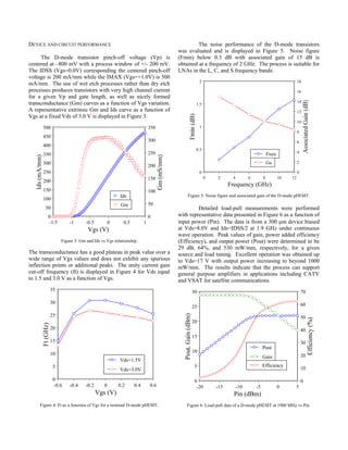
- Resulting devices demonstrate high performance metrics such as 25 GHz frequency, 90 GHz maximum frequency, and low noise figure below 0.3 dB.
![A 0.5-µm InGaP Etch Stop Power pHEMT Process Utilizing Multi-Level High
Density Interconnects
Walter A. Wohlmuth, Li Liu, Larry Witkowski, Rick Morton, Thorsten Saeger, Wolfgang Liebl, Mike
Fredd, Domingo Farías, Wayne Struble, Calvin Weichert, John Walkky, Steve Mahon, Otto Berger
TriQuint Semiconductor, 2300 N.E. Brookwood Pkwy., Hillsboro, OR 97124, wwohlmuth@tqs.com, 503-615-9236
Keywords: pHEMT, InGaP, BCB, D-mode
Abstract
A robust and highly manufacturable InGaP etch stop
pHEMT process with 0.5-µm gate lengths on 150 mm substrates
is presented. The process utilizes a double recess approach to
realize high breakdown, depletion-mode transistors with a
nominal gate to drain breakdown voltage of 17 V. The
transistors feature a nominal pinch-off voltage of –800 mV, on-
resistance of 1.8 ohm-mm, extrinisic transconductance of 350
mS/mm, off-capacitance of 0.3 pF/mm, unity current gain cut-
off frequency of 25 GHz, maximum frequency of oscillation of
90 GHz, and IDSS and IMAX values of 200 and 500 mA/mm,
respectively. Passive components include precision 50
ohm/square NiCr resistors, 280 ohm/square epitaxial N-
resistors, and 0.63 fF/um2
MIM capacitors. These devices are
integrated with TriQuint’s high density, planarized,
interconnect architecture enabling tremendous wiring flexibility
and packaging simplicity. The interconnect structure utilizes
benzocyclobutene (BCB) inter-metal dielectrics to form two
levels of thick, global interconnects in addition to one level of
local interconnect. This process, named TQPHT, is offered to
external customers through TriQuint Foundry Services for a
wide variety of applications including in part: high performance
GSM, CDMA, and WLAN switches, medium power amplifiers,
and low-noise amplifiers.
INTRODUCTION
In this paper we discuss the development of a 0.5-µm
InGaP etch stop pHEMT process on 150 mm wafers at
TriQuint Oregon. The development was driven by two
primary factors. The first factor was to transfer the 0.5-µm
AlAs etch stop power pHEMT process on 100 mm wafers
from Texas to Oregon fabrication facilities of TriQuint
converting directly to 150 mm wafers. This facilitated a high
volume, low cost solution available to both internal designers
and external customers through Foundry services. The
second factor involved the optimization of the process and
epitaxy technology for the creation of high performance
GSM, CDMA, and WLAN switch components, low-noise
amplifiers, and medium power amplifiers for both internal
and external customers. The technology transfer and
development also involved converting the interconnect
architecture to one that employs low-dielectric constant
materials based on benzocyclobutene.
PROCESS ARCHITECTURE
The process utilizes MBE on VGF, LEC, or VB
substrates. The growth sequence begins with the formation
of a superlattice buffer of alternating layers of GaAs and
AlGaAs deposited on the substrate. Unintentionally-doped
spacer layers of AlGaAs are placed on either side of the
unintentionally-doped InGaAs channel with Silicon delta-
doped layers placed on both sides of the channel-spacer layer
stack. A transition layer of AlGaAs is placed between the
lower spacer layer and the superlattice buffer to improve
noise performance. A Schottky layer of AlGaAs is placed on
top on the upper spacer layer to target the desired pinch-off
voltage and transconductance. An InGaP etch stop layer is
positioned on top of the Schottky layer followed by an upper
AlGaAs layer and then N+
GaAs ohmic contact layers. An
InGaP etch stop was used instead of an AlAs etch stop to
reduce device on-resistance and to obtain extremely high etch
selectivity [1]. The conduction band offset between the
AlGaAs and InGaP material systems is significantly less than
that between the AlAs and AlGaAs material systems,
permitting the use of a thicker etch stop layer. Typical room
temperature Hall measurements produced sheet carrier
concentrations of 3.15E12 cm-2
and electron mobility in
excess of 6500 cm2
/V•s.
Fabrication begins with the definition of fiducials
and wide recess openings. Upon formation of these features
a blanket film of plasma-assisted chemical vapor deposited
silicon dioxide (POX) is deposited to passivate and protect
the surface from physical and chemical damage during
subsequent process steps. Implant isolation is then
performed. The ohmic contacts are formed within dry etched
openings in the POX using AuGeNiAu alloyed at 400o
C.
Ohmic test is then performed to measure the ungated
transistor current, the ohmic contact resistance, the N+
layer
resistivity, and the N-
layer resistivity. The typical ohmic
contact resistance ranges from 0.10 to 0.15 ohm-mm due to
process variations. The N-
epitaxial resistors are formed
utilizing the openings formed by the wide recess etch.
Typical temperature coefficient of these resistors is 3000 ppm
per degree centigrade referenced to 25o
C with nominal sheet
resistance of 280 ohm/square. The gate feature is created
utilizing a TiPtAu metallization that is placed within dry](https://image.slidesharecdn.com/6276759f-b968-44b5-809c-ac057546d5af-150911160706-lva1-app6891/85/phempt-paper-7-1-1-320.jpg)
![etched openings in the POX. The narrow recess into the
AlGaAs material utilizes NH4OH:H2O2:H2O chemistry, which
provides excellent etch selectivity over InGaP and is a
standard wet etch chemistry used for MESFET processes at
TriQuint [2]. The InGaP etch stop is removed in HCl:H2O,
which has a high etch selectivity with respect to AlGaAs [1].
The gate metal is deposited and lifted off. Immediately after
gate formation a blanket coating of plasma-assisted chemical
vapor deposited silicon nitride (PSN) is deposited prior to
Nickel-Chromium (NiCr) thin film, high-precision resistor
formation. These resistors have a temperature coefficient that
is less than 100 ppm/o
C, referenced to 25o
C, over the –40 to
+125o
C temperature range, and possess a sheet resistance of
50 +/- 3 ohm/square. The maximum current and voltage
ratings of the NiCr resistors are 1.0 mA/µm and 50 mV/µm,
respectively. Another blanket coat of PSN is applied after
precision resistor formation for physical and chemical
protection of the NiCr prior to interconnect formation. The
first interconnect metal (Metal0) consists of TiPtAu
metallization and is used primarily as a local interconnect to
the device contacts of the transistors, varactors, resistors, and
Schottky diodes. This metal is also used as the bottom plate
of a high precision MIM capacitor. Another PSN layer is
then deposited to serve as the MIM capacitor dielectric prior
to the formation of the top plate of the MIM capacitor using a
TiPtAu metallization. The MIM dielectric is formed with a
100 nm thick PSN film possessing a relative permittivity of
6.8 and giving a capacitance per unit area of 0.63 +/- 0.10
fF/um2
. A final layer of PSN is deposited prior to proceeding
with the upper layers of global interconnects.
The interconnect architecture proceeds with the
application of a planarizing, interlevel dielectric composed of
benzocyclobutene (BCB). This dielectric is formed using
conventional spin-on techniques and then cured at low
temperature. Once cured, the material is mechanically tough,
exhibits less than 0.25% water absorption, and has a relative
permittivity of approximately 2.7. Inter-level vias are formed
using an Helicon plasma etch system. The vias are
electroplated along with metallic global interconnects.
Patterned field metal is used to delineate the global
interconnect metallic features. A thin dielectric layer of PSN
separates the BCB layers and encapsulates the metal1
features. Upon completion of Via1 and Metal1 a second set
of global interconnects are formed, Via2 and Metal2. The
substrate is then coated with a final passivation PSN layer
and bondpad via openings are formed to access test points on
devices and circuits. A representative schematic cross-
section of the process architecture is displayed in Figure 1.
The nominal thickness of Metal1 and Metal2 are 2.0 and 4.0
µm, respectively. The first layer of BCB is nominally 1.0 µm
thick and the second layer is nominally 2.8 µm thick. The
final passivation PSN is a total of 0.8 µm thick.
Figure 1: Schematic cross-section of the TQPHT process
A STEM image of a portion of the transistor and interconnect
architecture is displayed in Figure 2.
ILD PSN1
BCB1
Base dielectrics
BCB2
Metal0
Ohmic Gate
Figure 2: STEM cross-section of pHEMT process.
The excellent degree of planarization of the BCB can clearly
be seen over the gate, ohmic, and metal0 features. The base
dielectrics are composed of a combination of POX and PSN.
Also evident are the wide and narrow recess ledges. Upon
completion of front-side processing, the wafers can be treated
in a number of ways. These options include: thinning the
substrate down to thickness of 4, 7, or 10 mils; sawing out
die; and/or substrate via formation.
Detailed and thorough process qualification has been
completed and passed at wafer level and on packaged
products. The wafer level reliability testing included
autoclave at 121o
C, 100% relative humidity, and 15 psi for 96
hours, high temperature unbiased bake at 275o
C in air for 168
hours, and temperature cycle from –40 to +125o
C for 1000
cycles. The packaged product reliability testing included
HTOL under bias and at 150o
C junction temperature,
preconditioning, autoclave, HAST at 130o
C with 85% relative
humidity for 96 hours, temperature cycle, thermal shock, and
CDM and HBM ESD testing.](https://image.slidesharecdn.com/6276759f-b968-44b5-809c-ac057546d5af-150911160706-lva1-app6891/85/phempt-paper-7-1-2-320.jpg)
![A high power GSM switch for quad-band cellular
modules has been demonstrated in this process. The switch is
able to accommodate many different systems such as GSM,
E-GSM, PCS, and DCS and is leading a shift away from the
conventional PIN diodes as the selected component to switch
RF signals at the transmit/receive antenna port. PIN diodes
have high insertion loss and require high bias current relative
to pHEMT transistors enabling pHEMTs to become the
technology of choice for cellular phone handsets. The
insertion loss, 2nd
harmonic (H2) suppression, and 3rd
harmonic (H3) suppression levels for a single pole six throw
(SP6T) transmit/receive switch is displayed in Figure 7 at a
control voltage of 2.5V and a frequency of 915 MHz.
SP6T TQ4M4006
TX1 (Vctrl=2.5v F=915MHz)
-120
-110
-100
-90
-80
-70
-60
-50
-40
-30
-20
26 27 28 29 30 31 32 33 34 35 36
Input Power (dBm)
Harmonics(dBc)
-2.0
-1.8
-1.6
-1.4
-1.2
-1.0
-0.8
-0.6
-0.4
-0.2
0.0
InsertionLoss(dB)
H2H3
Loss
Figure 7: Harmonics suppression and insertion loss of a SP6T GSM switch at
2.5V control voltage.
This switch component is used for 850 MHz GSM, 900 MHz
GSM, 1800 MHz DCS, and 1900 MHz PCS systems with
separate arms for each receive band with the transmit arms
combining the GSM signals and the DCS and PCS signals
separately. State-of-the-art insertion loss and harmonic
suppression levels are achieved with this circuit.
A high power antenna switch in a single pole three
throw configuration has also been demonstrated in this
process. This switch is ideally suited to applications where
the antenna of a CDMA handset is to be routed to the Cellular
duplexer, the PCS duplexer and the GPS receiver input. The
switch provides optimized input 3rd
order intercept point
(IP3) and cross modulation for use in CDMA applications.
The input IP3 and current for a single pole three throw switch
is displayed in Figure 8 at a control voltage of 2.5 V and a
frequency of 837 MHz. World class single tone desense and
ESD robustness levels are achieved with this circuit.
TQP4M3007 CDMA SP3T
Tx to Antenna IIP3 (Vctrl = 2.7 V, T= 25 C)
Tx tones at 837 and 838 MHz
60
62
64
66
68
70
72
74
76
78
80
22.0 23.0 24.0 25.0 26.0
Total Tx Input Power (dBm)
IIP3(dBm)
0
5
10
15
20
25
30
35
40
45
50
Current(uA)
Figure 8: Input IP3 and control current for SP3T CDMA switch at 2.7V
control voltage.
CONCLUSIONS
A detailed description of the TQPHT process architecture has
been presented along with representative device and circuit
performance. This robust and highly manufactureable
process can be used for a wide variety of applications.
REFERENCES
[1] A. W. Hanson et al., GaAs IC Technical Digest, pp. 195-197, Nov.
1998.
[2] E. P. Finchem et al. GaAs MANTECH Technical Digest, pp. 163-166.
April 1994.
ACRONYMS
CATV: cable television amplifiers
CDM: charge device model
CDMA: coded division multiple access
DCS: digital communication system
E-GSM: enhanced global system for mobile communications
ESD: electrostatic discharge
GSM: global system for mobile communications
HAST: highly accelerated stress testing
HBM: human body model
HTOL: high temperature operating life
LEC: liquid encapsulated Czochralski
LNA: low-noise amplifiers
MESFET: metal-semiconductor field-effect transistor
PCS: personal communication system
PHEMT: pseudomorphic high-electron mobility transistor
STEM: scanning transmission electron microscopy
VB: vertical Bridgeman
VGF: vertical gradient freeze
VSAT: very small antenna terminals
WLAN: wireless local area network](https://image.slidesharecdn.com/6276759f-b968-44b5-809c-ac057546d5af-150911160706-lva1-app6891/85/phempt-paper-7-1-4-320.jpg)


