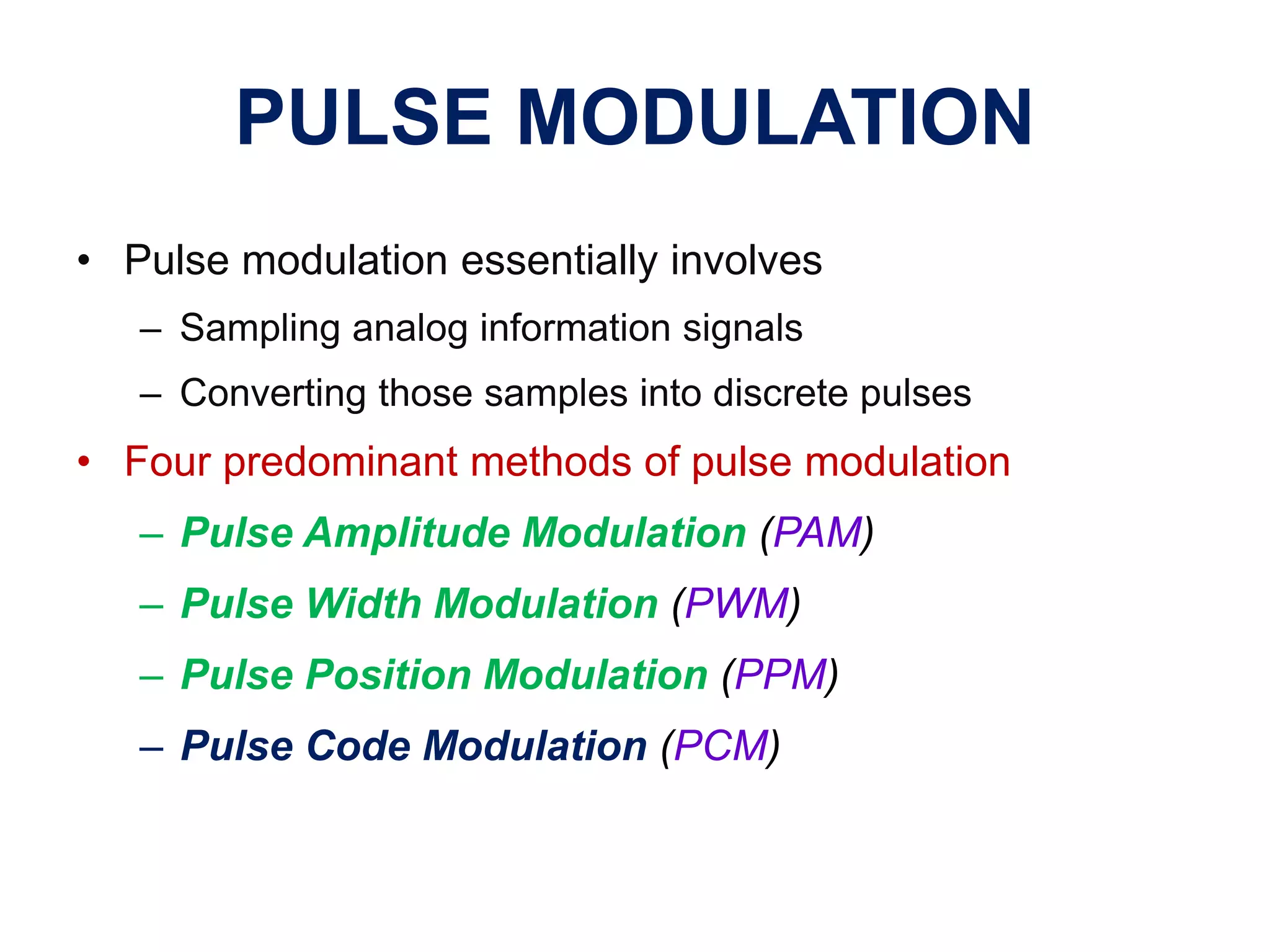
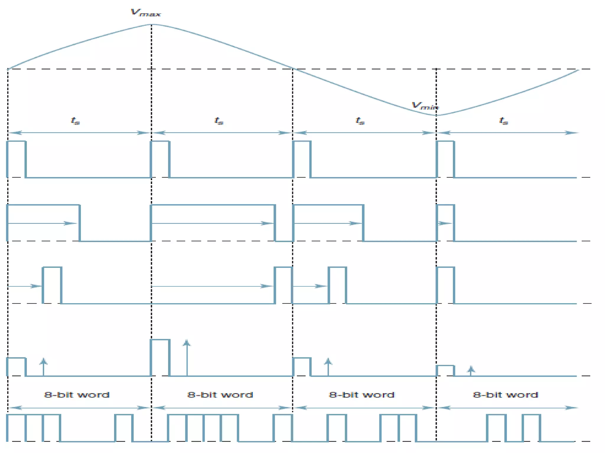
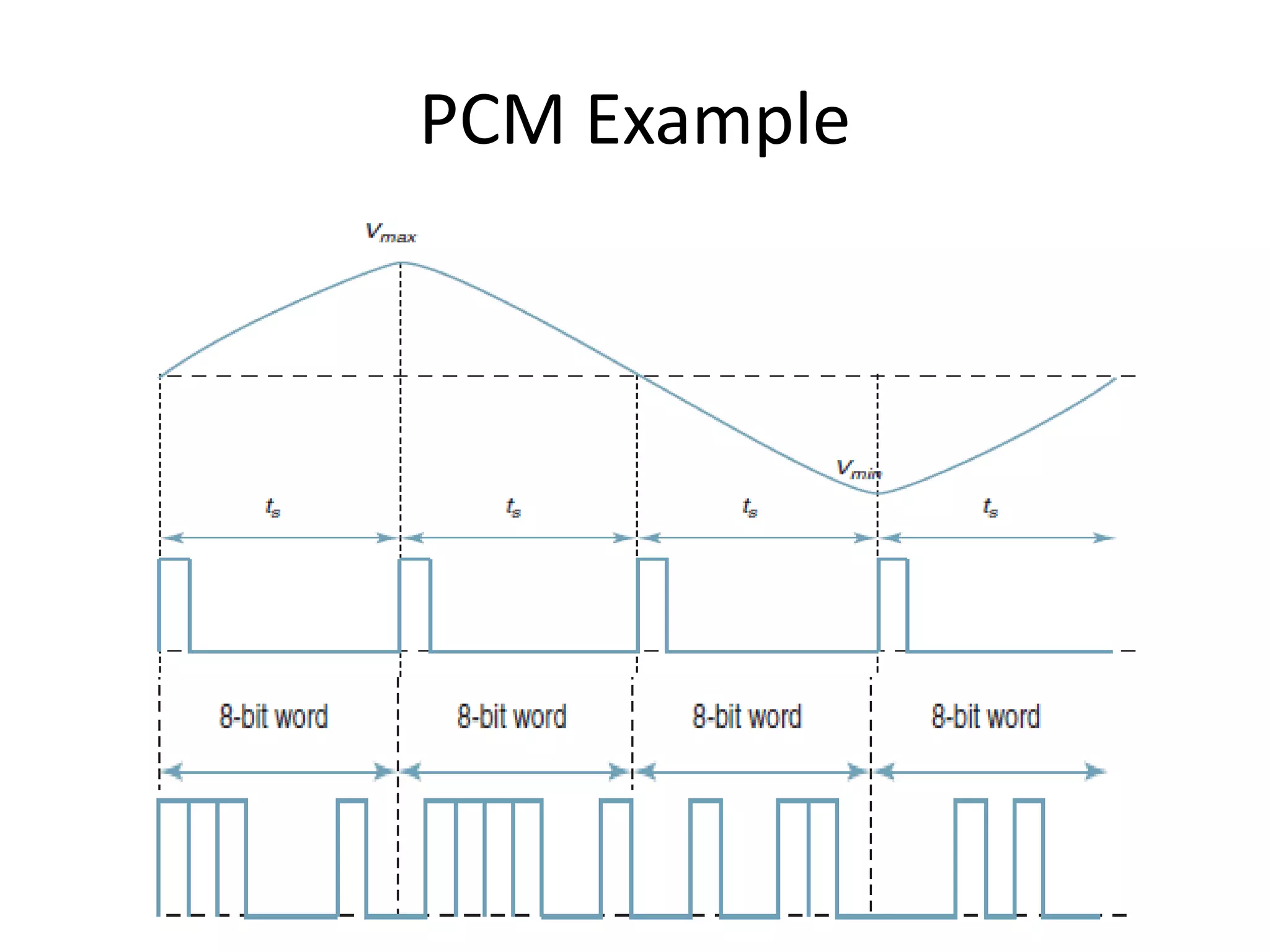
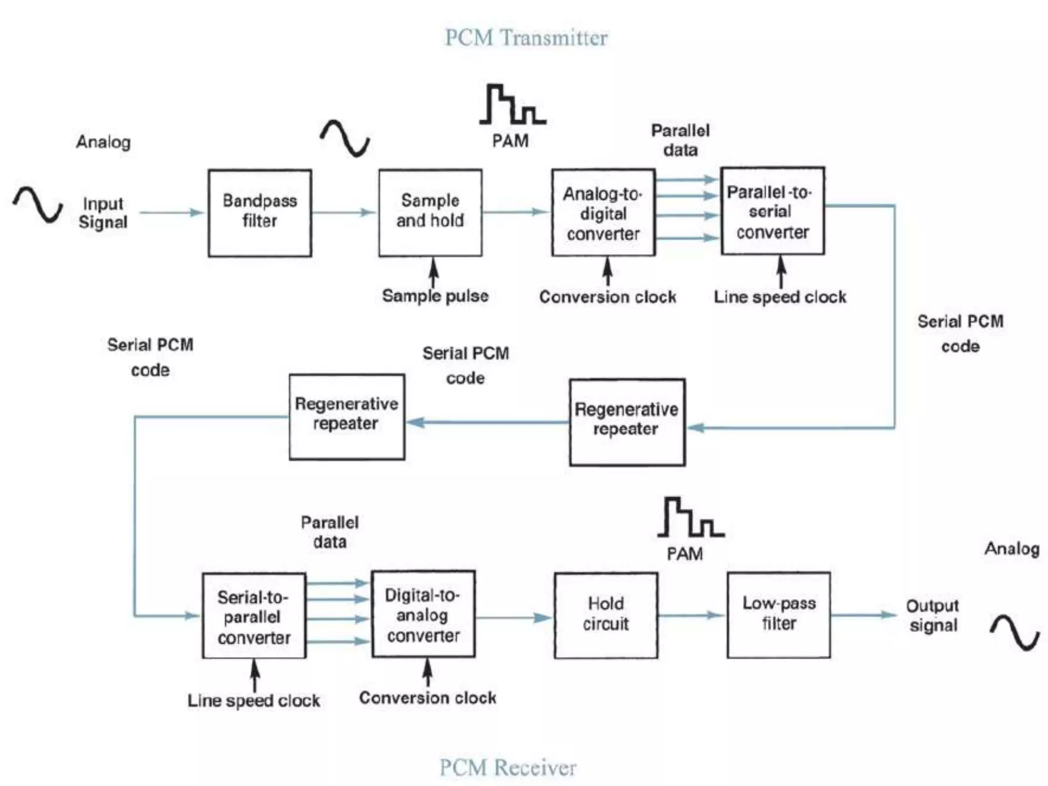
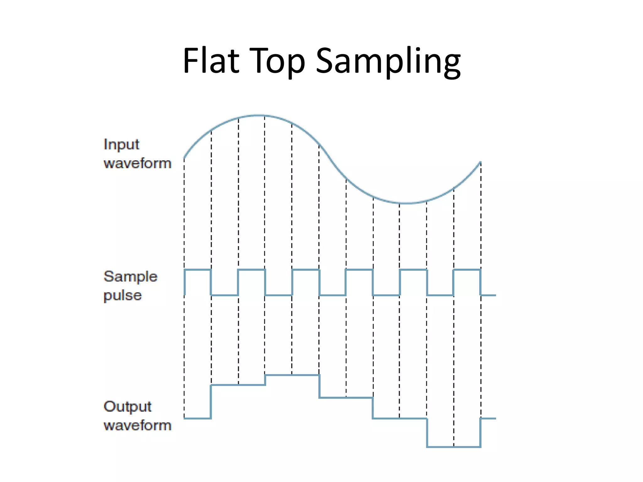
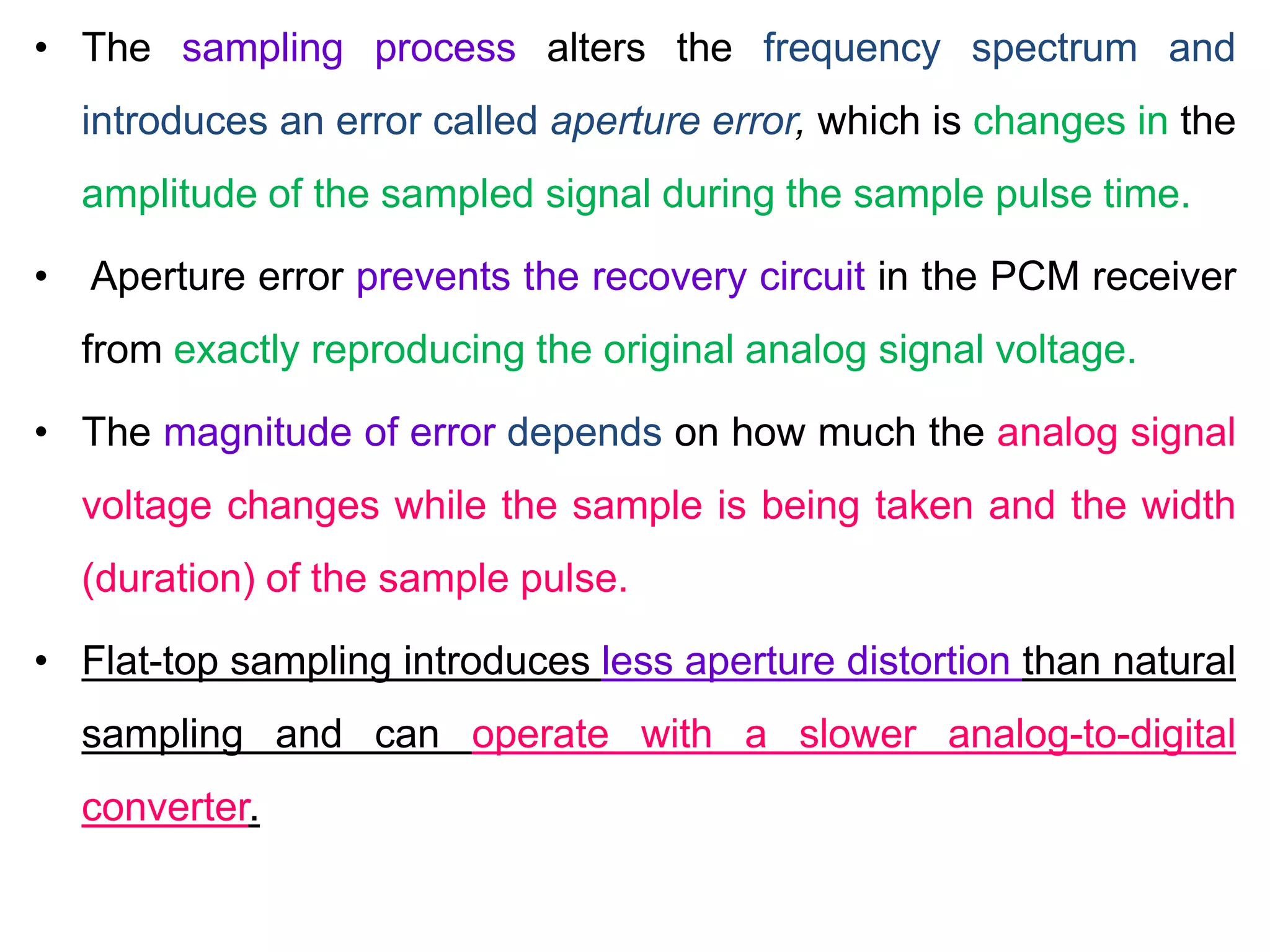
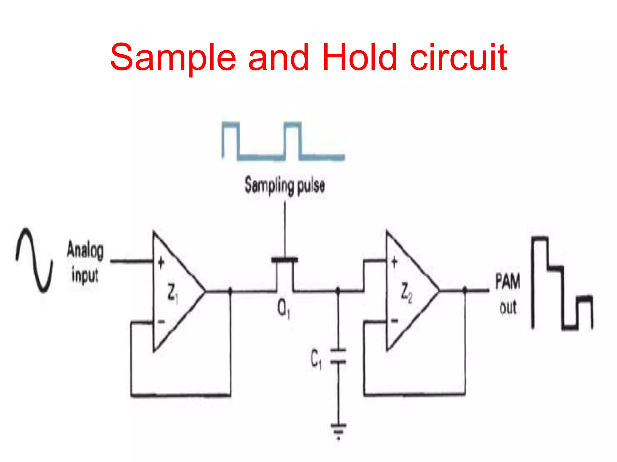
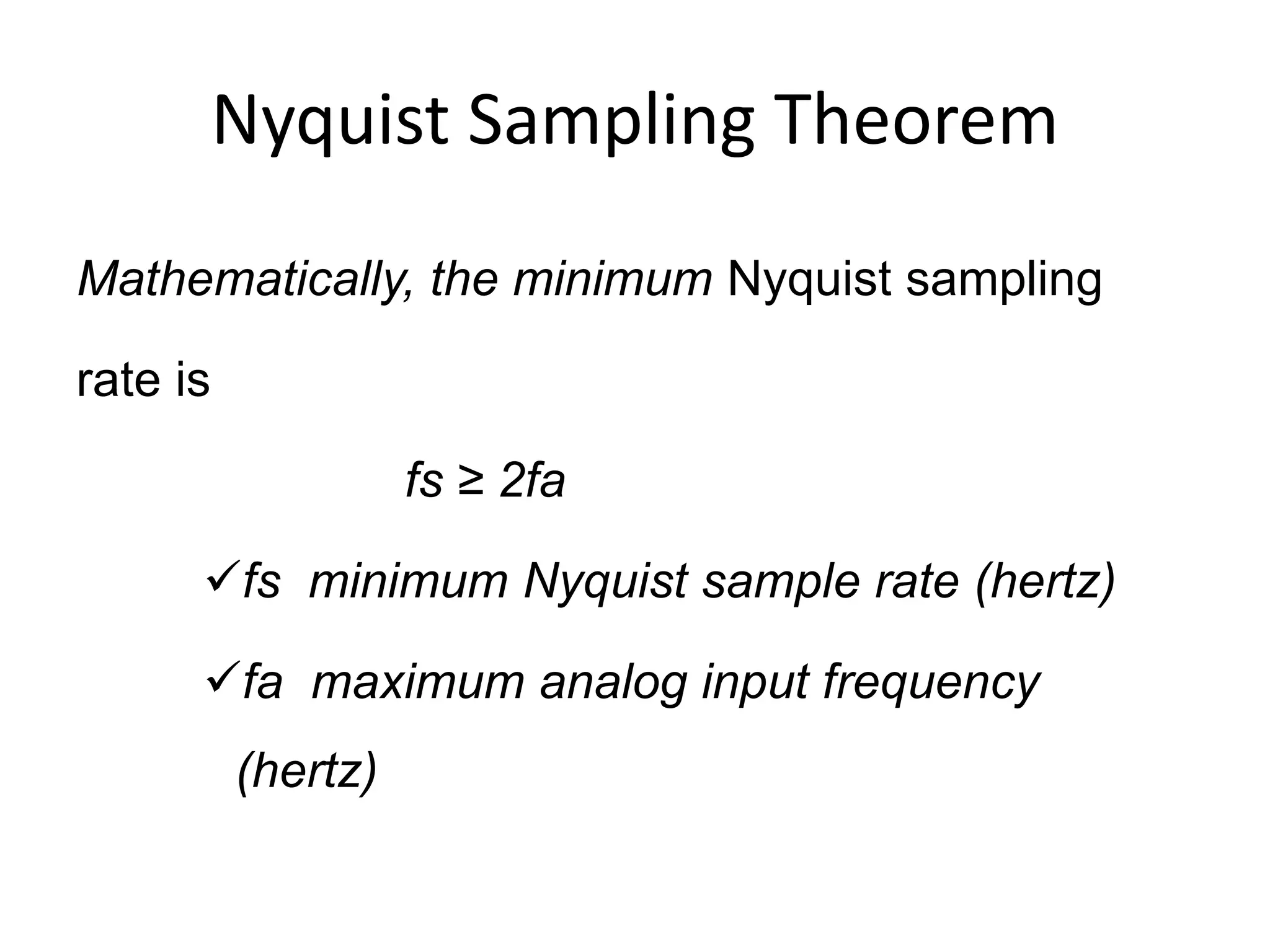
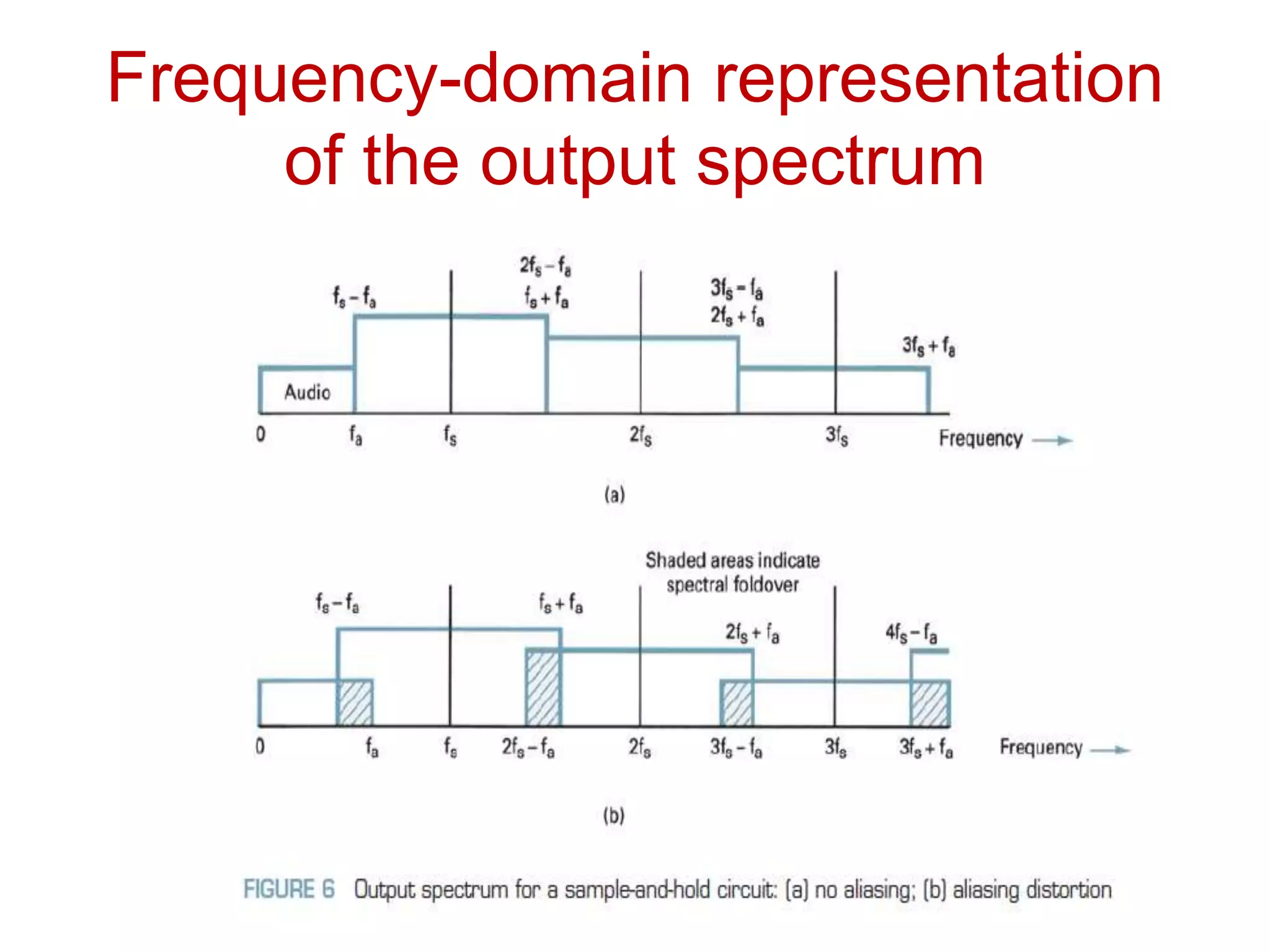
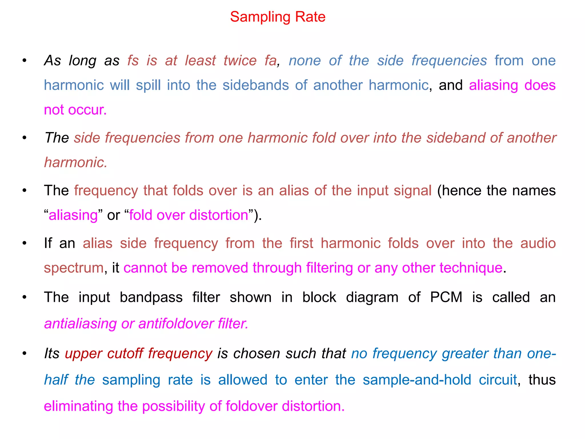
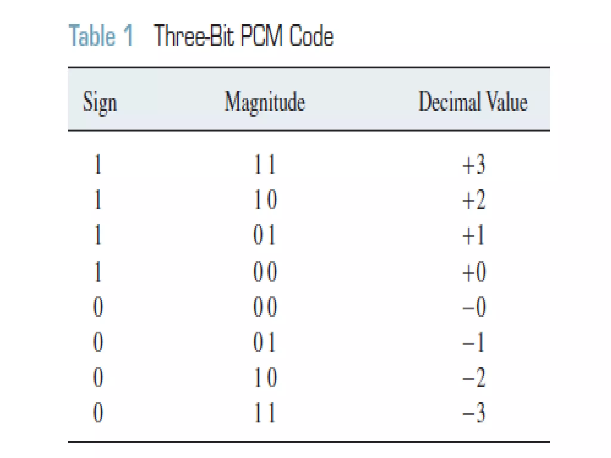
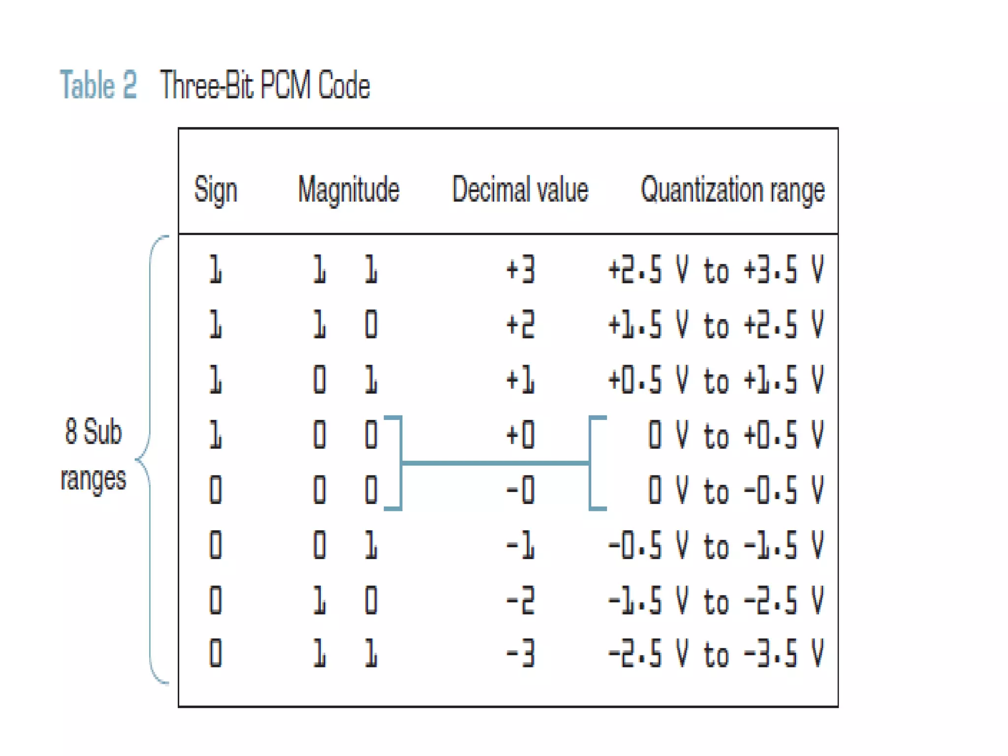
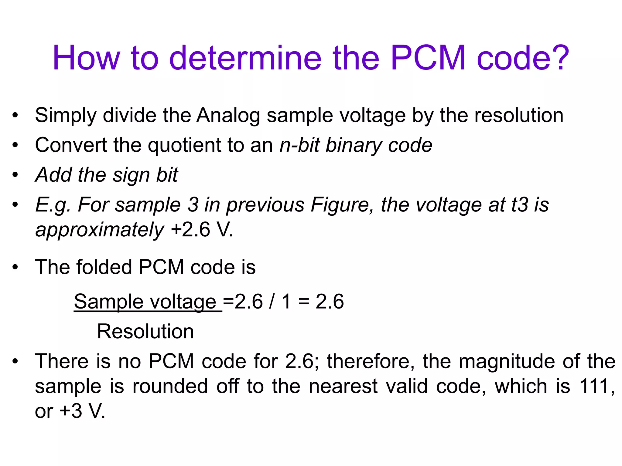
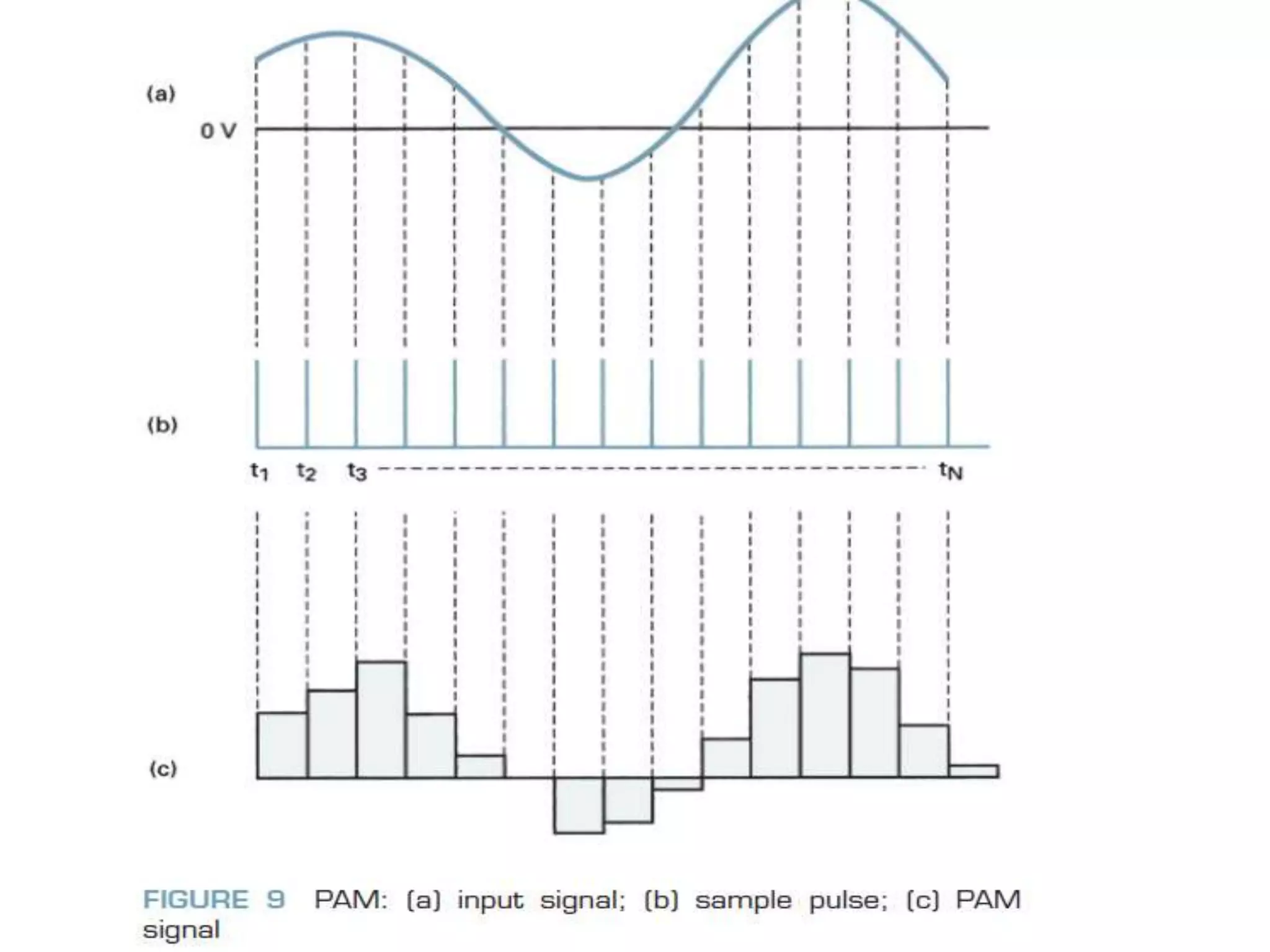
UNIT II
DIGITAL TRANSMISSION
Syllabus (Hours Planned = 10)
• Introduction to Pulse modulation
• Pulse Code Modulation
– PCM sampling
– Sampling Rate
– Quantization and Folded Binary Code
– Dynamic Range
– Signal-to-Quantization Noise Ratio
• Analog companding
• Digital companding
• Delta modulation
• Adaptive Delta Modulation
• Intersymbol interference
• Eye pattens
PULSE MODULATION
• Pulse modulation essentially involves
– Sampling analog information signals
– Converting those samples into discrete pulses
• Four predominant methods of pulse modulation
– Pulse Amplitude Modulation (PAM)
– Pulse Width Modulation (PWM)
– Pulse Position Modulation (PPM)
– Pulse Code Modulation (PCM)
Pulse Code Modulation (PCM)
• Most prevalent form of pulse modulation
• Used for commercial digital transmission systems.
• In PCM, the analog signal is sampled and then converted to a
serial n-bit binary code for transmission.
• Each code has the same number of bits and requires the
same length of time for transmission.
• The binary codes used for PCM are n-bit codes, where n may
be any positive integer greater than 1.
• In PCM, the pulses are of fixed length and fixed amplitude.
Pulse Code Modulation (PCM)
• PCM is the preferred method of communications within the Public
Switched Telephone Network (PSTN)
• PCM is a binary system where a pulse or lack of a pulse within a
prescribed time slot represents either a logic 1 or a logic 0
condition.
• With PCM, it is easy to combine digitized voice and digital data into
a single, high-speed digital signal and propagate it over either
metallic or optical fiber cables.
PCM Example
Single Channel Simplex PCM
Transmission System
Pulse Code Modulation (PCM)
• Bandpass Filter limits the frequency of the analog input signal
to the standard voice-band frequency range of 300 Hz to 3000
Hz.
• Sample-and-hold circuit periodically samples the analog input
signal and converts those samples to a multilevel PAM signal.
• Analog-to-digital Converter (ADC) converts the PAM samples
to parallel PCM codes, which are converted to serial binary
data in the parallel-to-serial converter and then outputted onto
the transmission line as serial digital pulses.
• Transmission line repeaters are placed at prescribed distances
to regenerate the digital pulses.
• Serial-to-parallel converter converts serial pulses received
from the transmission line to parallel PCM codes.
• Digital-to-analog Converter (DAC)
– converts the parallel PCM codes to multilevel PAM signals.
• Hold circuit
– basically a lowpass filter that converts the PAM signals back
to its original analog form.
• Codec (coder/decoder)
– An integrated circuit that performs the PCM encoding and
decoding functions is called a codec (coder/decoder)
Pulse Code Modulation (PCM)
PCM SAMPLING
• The function of a sampling circuit in a PCM transmitter
– To periodically sample the continually changing analog input
voltage
– Then convert those samples to a series of constant amplitude
pulses that can more easily be converted to binary PCM code.
• Impact of ADC Conversion Time
– For the ADC to accurately convert a voltage to a binary code,
the voltage must be relatively constant so that the ADC can
complete the conversion before the voltage level changes.
– If not, the ADC would be continually attempting to follow the
changes and may never stabilize on any PCM code.
Basic Techniques of Sampling
• Two basic techniques used to perform the
sampling function
–Natural Sampling
–Flat-top Sampling
Natural sampling
• The tops of the sample pulses retain their natural shape
during the sample interval
– It is difficult for an ADC to convert the sample to a PCM code.
• With natural sampling, the frequency spectrum of the sampled
output is different from that of an ideal sample.
• The amplitude of the frequency components produced from
narrow, finite-width sample pulses decreases for the higher
harmonics in a (sin x)/x manner.
• This alters the information frequency spectrum requiring the use of
frequency equalizers (compensation filters) before recovery by a
low-pass filter.
Natural Sampling
Flat Top Sampling
• Most common method used for sampling voice
signals in PCM systems is flat top sampling,
which is accomplished in a sample-and-hold
circuit.
• With flat-top sampling, the input voltage is
sampled with a narrow pulse and then held
relatively constant until the next sample is taken.
Flat Top Sampling
• The sampling process alters the frequency spectrum and
introduces an error called aperture error, which is changes in the
amplitude of the sampled signal during the sample pulse time.
• Aperture error prevents the recovery circuit in the PCM receiver
from exactly reproducing the original analog signal voltage.
• The magnitude of error depends on how much the analog signal
voltage changes while the sample is being taken and the width
(duration) of the sample pulse.
• Flat-top sampling introduces less aperture distortion than natural
sampling and can operate with a slower analog-to-digital
converter.
Sample and Hold circuit
Input and Output Waveforms
• FET acts as a simple analog switch.
• The time that transistor Q1 is on is called the
aperture or acquisition time
• When turned on, Q1 provides a low-impedance path
to deposit the analog sample voltage across
capacitor C1.
• Capacitor C1 is the hold circuit. When Q1 is off, C1
does not have a complete path to discharge through
and, therefore, stores the sampled voltage.
• If the input to the ADC is changing while it is performing
the conversion, aperture distortion results.
– By having a short aperture time and keeping the input
to the ADC relatively constant, the sample-and-hold
circuit can reduce aperture distortion.
• Output impedance of voltage follower Z1 and the on
resistance of Q1 must be as small as possible.
• The RC charging time constant of the capacitor is kept
very short, allowing the capacitor to charge or discharge
rapidly during the short acquisition time.
• The storage time of the capacitor is called
the A/D conversion time because it is during
this time that the ADC converts the sample
voltage to a PCM code.
• The acquisition time should be very short to
ensure that a minimum change occurs in
the analog signal while it is being deposited
across C1.
• Droop: Gradual discharge across the capacitor during
the conversion time.
– caused by the capacitor discharging through its own
leakage resistance and the input impedance of
voltage follower Z2.
• The input impedance of Z2 and the leakage resistance
of C1 be as high as possible.
• Essentially, voltage followers Z1 and Z2 isolate the
sample-and-hold circuit (Q1 and C1) from the input and
output circuitry.
Sampling Rate
• The Nyquist sampling theorem establishes the
minimum sampling rate (fs) that can be used for a
given PCM system.
• For a sample to be reproduced accurately in a PCM
receiver, each cycle of the analog input signal (fa)
must be sampled atleast twice.
• Consequently, the minimum sampling rate is equal to
twice the highest audio input frequency.
• If fs is less than two times fa, an impairment called
alias or foldover distortion occurs.
Nyquist Sampling Theorem
Mathematically, the minimum Nyquist sampling
rate is
fs ≥ 2fa
fs minimum Nyquist sample rate (hertz)
fa maximum analog input frequency
(hertz)
• A sample-and-hold circuit is a nonlinear device (mixer) with two inputs: the sampling
pulse and the analog input signal.
– Nonlinear mixing (heterodyning) occurs between these two signals.
– output includes the two original inputs (the audio and the fundamental frequency
of the sampling pulse), their sum and difference frequencies (fs± fa), all the
harmonics of fs and fa (2fs, 2fa, 3fs, 3fa,etc)and their associated cross products
(2fs±fa, 3fs±fa,etc).
• The sampling pulse is a repetitive waveform, it is made up of a series of harmonically
related sine waves.
• Each of these sine waves is amplitude modulated by the analog signal and produces
sum and difference frequencies symmetrical around each of the harmonics of fs.
• Each sum and difference frequency generated is separated from its respective center
frequency by fa.
Frequency-domain representation
of the output spectrum
• As long as fs is at least twice fa, none of the side frequencies from one
harmonic will spill into the sidebands of another harmonic, and aliasing does
not occur.
• The side frequencies from one harmonic fold over into the sideband of another
harmonic.
• The frequency that folds over is an alias of the input signal (hence the names
“aliasing” or “fold over distortion”).
• If an alias side frequency from the first harmonic folds over into the audio
spectrum, it cannot be removed through filtering or any other technique.
• The input bandpass filter shown in block diagram of PCM is called an
antialiasing or antifoldover filter.
• Its upper cutoff frequency is chosen such that no frequency greater than one-
half the sampling rate is allowed to enter the sample-and-hold circuit, thus
eliminating the possibility of foldover distortion.
Sampling Rate
PCM Codes
• The codes currently used for PCM are sign-magnitude
codes,
– The most significant bit (MSB) is the sign bit
– Remaining bits are used for magnitude representation.
• The most significant bit is used to represent the sign of
the sample (logic 1 positive and logic 0 negative).
• The two remaining bits represent the magnitude.
– With two magnitude bits, there are four codes possible for positive
numbers and four codes possible for negative numbers.
• Consequently, there is a total of eight possible codes.
Quantization and the Folded
Binary Code
• Analog signals contain an infinite number of amplitude
possibilities.
• Quantization is the process of converting an infinite
number of possibilities to a finite number of conditions.
• Thus, converting an analog signal to a PCM code with
a limited number of combinations requires
quantization.
• In essence, quantization is the process of rounding off
the amplitudes of flat-top samples to a manageable
number of levels.
Quantization Example
• For example, a sine wave with a peak amplitude of
5 V varies between +5 V and -5 V passing through
every possible amplitude in between.
• A PCM code could have only eight bits, which
equates to only 28, or 256 combinations.
• Obviously, to convert samples of a sine wave to
PCM requires some rounding off.
• The leftmost bit is the sign bit (1 = + and 0 = -), and the two
rightmost bits represent magnitude.
• This type of code is called a folded binary code because the codes
on the bottom half of the table are a mirror image of the codes on
the top half, except for the sign bit.
• If the negative codes were folded over on top of the positive codes,
they would match perfectly.
• With a folded binary code, each voltage level has one code
assigned to it except zero volts, which has two codes, 100 (0) and
000 (0).
• The magnitude difference between adjacent steps is called the
quantization interval or quantum.
• The quantization interval is 1 V.
• For this code, the maximum signal magnitude that can be
encoded is +3 V (111) or -3 V (011), and the minimum signal
magnitude is +1 V (101) or -1 V(001).
• If the magnitude of the sample exceeds the highest
quantization interval, overload distortion (also called peak
limiting) occurs.
• Assigning PCM codes to absolute magnitudes is called
quantizing.
Resolution
• Resolution - The magnitude of a quantum
• Resolution is equal to the voltage of the
minimum step size, which is equal to the
voltage of the least significant bit (Vlsb) of the
PCM code.
• The resolution is the minimum voltage other than
0 V that can be decoded by the digital-to-analog
converter in the receiver.
• The smaller the magnitude of a quantum, the
better (smaller) the resolution and the more
accurately the quantized signal will resemble the
original analog sample.
• With reference to previous table, each three-bit code has a
range of input voltages that will be converted to that code.
• For example, any voltage between +0.5 and +1.5 will be
converted to the code 101 (+1 V).
• Each code has a quantization range equal to + or - one-half
the magnitude of a quantum except the codes for +0 and -0.
• The 0-V codes each have an input range equal to only one-half
a quantum (0.5 V).
Quantization Error
• The likelihood of a sample voltage being equal to one of the eight quantization
levels is remote.
• Each sample voltage is rounded off (quantized) to the closest available
level and then converted to its corresponding PCM code.
• The PAM signal in the transmitter is essentially the same PAM signal produced
in the receiver.
• Any round-off errors in the transmitted signal are reproduced when the code is
converted back to analog in the receiver. This error is called the
QUANTIZATION ERROR (QE).
• The quantization error is equivalent to additive white noise as it alters the
signal amplitude.
• Consequently, quantization error is also called quantization noise
(Qn).
• The maximum magnitude for the quantization error is equal to one
half a quantum (0.5 V for the code shown in previous Table).
• The first sample occurs at time t1, when the input voltage is exactly 2
V.
• The PCM code that corresponds to +2 V is 110, and there is no
quantization error.
• Sample 2 occurs at time t2, when the input voltage is -1 V. The
corresponding PCM code is 001, and again there is no quantization
error.
Quantization Error
How to determine the PCM code?
• Simply divide the Analog sample voltage by the resolution
• Convert the quotient to an n-bit binary code
• Add the sign bit
• E.g. For sample 3 in previous Figure, the voltage at t3 is
approximately +2.6 V.
• The folded PCM code is
Sample voltage =2.6 / 1 = 2.6
Resolution
• There is no PCM code for 2.6; therefore, the magnitude of the
sample is rounded off to the nearest valid code, which is 111,
or +3 V.
• The rounding-off process results in a quantization error of 0.4 V.
• The quantized signal at best only roughly resembles the original
analog input signal.
– Because with a three-bit PCM code, the resolution is rather
poor and also because there are only three samples taken of
the analog signal.
• The quality of the PAM signal can be improved by using a PCM
code with more bits, reducing the magnitude of a quantum and
improving the resolution.
• The quality can also be improved by sampling the analog signal
at a faster rate.

PCM-Part 1.pptx

  • 1.
  • 2.
    Syllabus (Hours Planned= 10) • Introduction to Pulse modulation • Pulse Code Modulation – PCM sampling – Sampling Rate – Quantization and Folded Binary Code – Dynamic Range – Signal-to-Quantization Noise Ratio • Analog companding • Digital companding • Delta modulation • Adaptive Delta Modulation • Intersymbol interference • Eye pattens
  • 3.
    PULSE MODULATION • Pulsemodulation essentially involves – Sampling analog information signals – Converting those samples into discrete pulses • Four predominant methods of pulse modulation – Pulse Amplitude Modulation (PAM) – Pulse Width Modulation (PWM) – Pulse Position Modulation (PPM) – Pulse Code Modulation (PCM)
  • 5.
    Pulse Code Modulation(PCM) • Most prevalent form of pulse modulation • Used for commercial digital transmission systems. • In PCM, the analog signal is sampled and then converted to a serial n-bit binary code for transmission. • Each code has the same number of bits and requires the same length of time for transmission. • The binary codes used for PCM are n-bit codes, where n may be any positive integer greater than 1. • In PCM, the pulses are of fixed length and fixed amplitude.
  • 6.
    Pulse Code Modulation(PCM) • PCM is the preferred method of communications within the Public Switched Telephone Network (PSTN) • PCM is a binary system where a pulse or lack of a pulse within a prescribed time slot represents either a logic 1 or a logic 0 condition. • With PCM, it is easy to combine digitized voice and digital data into a single, high-speed digital signal and propagate it over either metallic or optical fiber cables.
  • 7.
  • 8.
    Single Channel SimplexPCM Transmission System
  • 10.
    Pulse Code Modulation(PCM) • Bandpass Filter limits the frequency of the analog input signal to the standard voice-band frequency range of 300 Hz to 3000 Hz. • Sample-and-hold circuit periodically samples the analog input signal and converts those samples to a multilevel PAM signal. • Analog-to-digital Converter (ADC) converts the PAM samples to parallel PCM codes, which are converted to serial binary data in the parallel-to-serial converter and then outputted onto the transmission line as serial digital pulses. • Transmission line repeaters are placed at prescribed distances to regenerate the digital pulses.
  • 11.
    • Serial-to-parallel converterconverts serial pulses received from the transmission line to parallel PCM codes. • Digital-to-analog Converter (DAC) – converts the parallel PCM codes to multilevel PAM signals. • Hold circuit – basically a lowpass filter that converts the PAM signals back to its original analog form. • Codec (coder/decoder) – An integrated circuit that performs the PCM encoding and decoding functions is called a codec (coder/decoder) Pulse Code Modulation (PCM)
  • 12.
  • 13.
    • The functionof a sampling circuit in a PCM transmitter – To periodically sample the continually changing analog input voltage – Then convert those samples to a series of constant amplitude pulses that can more easily be converted to binary PCM code. • Impact of ADC Conversion Time – For the ADC to accurately convert a voltage to a binary code, the voltage must be relatively constant so that the ADC can complete the conversion before the voltage level changes. – If not, the ADC would be continually attempting to follow the changes and may never stabilize on any PCM code.
  • 14.
    Basic Techniques ofSampling • Two basic techniques used to perform the sampling function –Natural Sampling –Flat-top Sampling
  • 15.
    Natural sampling • Thetops of the sample pulses retain their natural shape during the sample interval – It is difficult for an ADC to convert the sample to a PCM code. • With natural sampling, the frequency spectrum of the sampled output is different from that of an ideal sample. • The amplitude of the frequency components produced from narrow, finite-width sample pulses decreases for the higher harmonics in a (sin x)/x manner. • This alters the information frequency spectrum requiring the use of frequency equalizers (compensation filters) before recovery by a low-pass filter.
  • 16.
  • 17.
    Flat Top Sampling •Most common method used for sampling voice signals in PCM systems is flat top sampling, which is accomplished in a sample-and-hold circuit. • With flat-top sampling, the input voltage is sampled with a narrow pulse and then held relatively constant until the next sample is taken.
  • 18.
  • 19.
    • The samplingprocess alters the frequency spectrum and introduces an error called aperture error, which is changes in the amplitude of the sampled signal during the sample pulse time. • Aperture error prevents the recovery circuit in the PCM receiver from exactly reproducing the original analog signal voltage. • The magnitude of error depends on how much the analog signal voltage changes while the sample is being taken and the width (duration) of the sample pulse. • Flat-top sampling introduces less aperture distortion than natural sampling and can operate with a slower analog-to-digital converter.
  • 20.
  • 21.
  • 22.
  • 23.
    • FET actsas a simple analog switch. • The time that transistor Q1 is on is called the aperture or acquisition time • When turned on, Q1 provides a low-impedance path to deposit the analog sample voltage across capacitor C1. • Capacitor C1 is the hold circuit. When Q1 is off, C1 does not have a complete path to discharge through and, therefore, stores the sampled voltage.
  • 24.
    • If theinput to the ADC is changing while it is performing the conversion, aperture distortion results. – By having a short aperture time and keeping the input to the ADC relatively constant, the sample-and-hold circuit can reduce aperture distortion. • Output impedance of voltage follower Z1 and the on resistance of Q1 must be as small as possible. • The RC charging time constant of the capacitor is kept very short, allowing the capacitor to charge or discharge rapidly during the short acquisition time.
  • 25.
    • The storagetime of the capacitor is called the A/D conversion time because it is during this time that the ADC converts the sample voltage to a PCM code. • The acquisition time should be very short to ensure that a minimum change occurs in the analog signal while it is being deposited across C1.
  • 26.
    • Droop: Gradualdischarge across the capacitor during the conversion time. – caused by the capacitor discharging through its own leakage resistance and the input impedance of voltage follower Z2. • The input impedance of Z2 and the leakage resistance of C1 be as high as possible. • Essentially, voltage followers Z1 and Z2 isolate the sample-and-hold circuit (Q1 and C1) from the input and output circuitry.
  • 27.
  • 28.
    • The Nyquistsampling theorem establishes the minimum sampling rate (fs) that can be used for a given PCM system. • For a sample to be reproduced accurately in a PCM receiver, each cycle of the analog input signal (fa) must be sampled atleast twice. • Consequently, the minimum sampling rate is equal to twice the highest audio input frequency. • If fs is less than two times fa, an impairment called alias or foldover distortion occurs.
  • 29.
    Nyquist Sampling Theorem Mathematically,the minimum Nyquist sampling rate is fs ≥ 2fa fs minimum Nyquist sample rate (hertz) fa maximum analog input frequency (hertz)
  • 30.
    • A sample-and-holdcircuit is a nonlinear device (mixer) with two inputs: the sampling pulse and the analog input signal. – Nonlinear mixing (heterodyning) occurs between these two signals. – output includes the two original inputs (the audio and the fundamental frequency of the sampling pulse), their sum and difference frequencies (fs± fa), all the harmonics of fs and fa (2fs, 2fa, 3fs, 3fa,etc)and their associated cross products (2fs±fa, 3fs±fa,etc). • The sampling pulse is a repetitive waveform, it is made up of a series of harmonically related sine waves. • Each of these sine waves is amplitude modulated by the analog signal and produces sum and difference frequencies symmetrical around each of the harmonics of fs. • Each sum and difference frequency generated is separated from its respective center frequency by fa.
  • 31.
  • 32.
    • As longas fs is at least twice fa, none of the side frequencies from one harmonic will spill into the sidebands of another harmonic, and aliasing does not occur. • The side frequencies from one harmonic fold over into the sideband of another harmonic. • The frequency that folds over is an alias of the input signal (hence the names “aliasing” or “fold over distortion”). • If an alias side frequency from the first harmonic folds over into the audio spectrum, it cannot be removed through filtering or any other technique. • The input bandpass filter shown in block diagram of PCM is called an antialiasing or antifoldover filter. • Its upper cutoff frequency is chosen such that no frequency greater than one- half the sampling rate is allowed to enter the sample-and-hold circuit, thus eliminating the possibility of foldover distortion. Sampling Rate
  • 33.
  • 35.
    • The codescurrently used for PCM are sign-magnitude codes, – The most significant bit (MSB) is the sign bit – Remaining bits are used for magnitude representation. • The most significant bit is used to represent the sign of the sample (logic 1 positive and logic 0 negative). • The two remaining bits represent the magnitude. – With two magnitude bits, there are four codes possible for positive numbers and four codes possible for negative numbers. • Consequently, there is a total of eight possible codes.
  • 36.
    Quantization and theFolded Binary Code
  • 37.
    • Analog signalscontain an infinite number of amplitude possibilities. • Quantization is the process of converting an infinite number of possibilities to a finite number of conditions. • Thus, converting an analog signal to a PCM code with a limited number of combinations requires quantization. • In essence, quantization is the process of rounding off the amplitudes of flat-top samples to a manageable number of levels.
  • 38.
    Quantization Example • Forexample, a sine wave with a peak amplitude of 5 V varies between +5 V and -5 V passing through every possible amplitude in between. • A PCM code could have only eight bits, which equates to only 28, or 256 combinations. • Obviously, to convert samples of a sine wave to PCM requires some rounding off.
  • 40.
    • The leftmostbit is the sign bit (1 = + and 0 = -), and the two rightmost bits represent magnitude. • This type of code is called a folded binary code because the codes on the bottom half of the table are a mirror image of the codes on the top half, except for the sign bit. • If the negative codes were folded over on top of the positive codes, they would match perfectly. • With a folded binary code, each voltage level has one code assigned to it except zero volts, which has two codes, 100 (0) and 000 (0). • The magnitude difference between adjacent steps is called the quantization interval or quantum.
  • 41.
    • The quantizationinterval is 1 V. • For this code, the maximum signal magnitude that can be encoded is +3 V (111) or -3 V (011), and the minimum signal magnitude is +1 V (101) or -1 V(001). • If the magnitude of the sample exceeds the highest quantization interval, overload distortion (also called peak limiting) occurs. • Assigning PCM codes to absolute magnitudes is called quantizing.
  • 42.
    Resolution • Resolution -The magnitude of a quantum • Resolution is equal to the voltage of the minimum step size, which is equal to the voltage of the least significant bit (Vlsb) of the PCM code. • The resolution is the minimum voltage other than 0 V that can be decoded by the digital-to-analog converter in the receiver. • The smaller the magnitude of a quantum, the better (smaller) the resolution and the more accurately the quantized signal will resemble the original analog sample.
  • 43.
    • With referenceto previous table, each three-bit code has a range of input voltages that will be converted to that code. • For example, any voltage between +0.5 and +1.5 will be converted to the code 101 (+1 V). • Each code has a quantization range equal to + or - one-half the magnitude of a quantum except the codes for +0 and -0. • The 0-V codes each have an input range equal to only one-half a quantum (0.5 V).
  • 44.
    Quantization Error • Thelikelihood of a sample voltage being equal to one of the eight quantization levels is remote. • Each sample voltage is rounded off (quantized) to the closest available level and then converted to its corresponding PCM code. • The PAM signal in the transmitter is essentially the same PAM signal produced in the receiver. • Any round-off errors in the transmitted signal are reproduced when the code is converted back to analog in the receiver. This error is called the QUANTIZATION ERROR (QE). • The quantization error is equivalent to additive white noise as it alters the signal amplitude.
  • 46.
    • Consequently, quantizationerror is also called quantization noise (Qn). • The maximum magnitude for the quantization error is equal to one half a quantum (0.5 V for the code shown in previous Table). • The first sample occurs at time t1, when the input voltage is exactly 2 V. • The PCM code that corresponds to +2 V is 110, and there is no quantization error. • Sample 2 occurs at time t2, when the input voltage is -1 V. The corresponding PCM code is 001, and again there is no quantization error. Quantization Error
  • 47.
    How to determinethe PCM code? • Simply divide the Analog sample voltage by the resolution • Convert the quotient to an n-bit binary code • Add the sign bit • E.g. For sample 3 in previous Figure, the voltage at t3 is approximately +2.6 V. • The folded PCM code is Sample voltage =2.6 / 1 = 2.6 Resolution • There is no PCM code for 2.6; therefore, the magnitude of the sample is rounded off to the nearest valid code, which is 111, or +3 V.
  • 49.
    • The rounding-offprocess results in a quantization error of 0.4 V. • The quantized signal at best only roughly resembles the original analog input signal. – Because with a three-bit PCM code, the resolution is rather poor and also because there are only three samples taken of the analog signal. • The quality of the PAM signal can be improved by using a PCM code with more bits, reducing the magnitude of a quantum and improving the resolution. • The quality can also be improved by sampling the analog signal at a faster rate.