
Recommended
More Related Content
What's hot
What's hot (20)
Similar to Original Opto PC815 LTV815 V815 815 DIP-4 New
Similar to Original Opto PC815 LTV815 V815 815 DIP-4 New (20)
More from authelectroniccom
More from authelectroniccom (20)
Recently uploaded
Recently uploaded (20)
Original Opto PC815 LTV815 V815 815 DIP-4 New
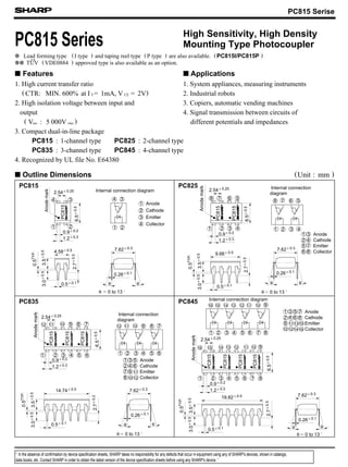
- 1. PC815 Series High Sensitivity, High Density Mounting Type Photocoupler s Features s Applications 1. High current transfer ratio ( CTR: MIN. 600% at I F= 1mA, V CE = 2V) 2. High isolation voltage between input and output ( V 3. Compact dual-in-line package 1. System appliances, measuring instruments 2. Industrial robots 3. Copiers, automatic vending machines 4. Signal transmission between circuits of different potentials and impedances s Outline Dimensions (Unit : mm ) data books, etc. Contact SHARP in order to obtain the latest version of the device specification sheets before using any SHARP's device.” “ In the absence of confirmation by device specification sheets, SHARP takes no responsibility for any defects that occur in equipment using any of SHARP's devices, shown in catalogs, PC815 : 1-channel type PC825 : 2-channel type PC835 : 3-channel type PC845 : 4-channel type 4. Recognized by UL file No. E64380 θ θ θ θ PC845 PC815 Anodemark PC815 PC815 PC815 PC815 PC815 Anodemark PC815 Internal connection diagram PC835 PC825 diagram Internal connection PC815 Anodemark PC815 34 21 4 3 Anodemark 1 2 PC815 PC815 1 1 Anode 2 Cathode 3 Emitter 4 Collector 9 2 3 4 5 6 7 8 1 2 3 4 5 6 7 8 9 1 2 3 4 5 6 9 8 7 1 2 3 4 5 6 9 8 7 8 7 6 5 1 2 3 4 1 2 3 4 8 7 6 5 Internal connection diagram 1 3 Anode 2 4 Cathode 5 7 Emitter 6 8 Collector Internal connection diagram 1 3 5 7 Anode 2 4 6 8 Cathode 9 Emitter Collector 1 3 5 Anode 2 4 6 Cathode 7 9 Emitter 8 Collector iso PC815 Serise θ θθ θ g Lead forming type (I type ) and taping reel type (P type ) are also available. (PC815I/PC815P ) : 5 000V rms ) 6.5±0.5 2.54± 0.25 1.2± 0.3 0.9± 0.2 4.58± 0.5 2.7±0.5 3.5±0.53.0±0.5 0.5TYP. 0.5± 0.1 7.62± 0.3 0.26± 0.1 θ = 0 to 13 ˚ θ = 0 to 13 ˚ 2.54± 0.25 6.5±0.5 1.2± 0.3 0.9± 0.2 14.74± 0.5 2.7±0.2 0.5± 0.1 0.5TYP. 3.5±0.53.0±0.5 7.62± 0.3 0.26± 0.1 θ = 0 to 13 ˚ 2.54± 0.25 6.5±0.5 1.2± 0.3 0.9± 0.2 0.5± 0.1 2.7±0.5 19.82± 0.5 0.5TYP. 3.5±0.53.0±0.5 7.62± 0.3 0.26± 0.1 θ = 0 to 13 ˚ 2.54± 0.25 1.2± 0.3 0.9± 0.2 6.5±0.5 0.5± 0.1 2.7±0.5 9.66± 0.5 0.5TYP. 3.5±0.53.0±0.5 7.62± 0.3 0.26± 0.1 gg TUV (VDE0884 ) approved type is also available as an option. .. 111213141516 111213141516 11 12 13 14 15 16 11 11 121112 12 10 10 10 10 10 10
- 2. PC815 Series *1 Pulse width<=100 µ s, Duty ratio : 0.001 *3 For 10 seconds Parameter Symbol MIN. TYP. MAX. Unit Input VF - 1.2 1.4 V V FM - - 3.0 V IR - - 10 µ A Ct - 30 250 pF Output ICEO - - 10 - 6 A Transfer charac- teristics CTR 600 % VCE(sat) - 0.8 1.0 V 5 x 10 10 10 11 - Ω 0.6 1.0 pF 1 6 - kHz - - 60 300 µ s - 53 250 µ s s Absolute Maximum Ratings (Ta= 25˚C) s Electro-optical Characteristics (Ta= 25˚C) Parameter Symbol Rating Unit Input Forward current IF 50 mA *1 Peak forward current IFM 1 A Reverse voltage VR 6 V Power dissipation P 70 mW Output Collector-emitter voltage V CEO 35 V Emitter-collector voltage V ECO 6 V Collector current IC 80 mA Collector power dissipation PC 150 mW Total power dissipation P tot 200 mW *2 Isolation voltage V iso Operating temperature T opr - 30 to + 100 ˚C Storage temperature T stg - 55 to + 125 ˚C *3 Soldering temperature T sol 260 ˚C Forward voltage Peak forward voltage Reverse current Terminal capacitance Collector dark current Current transfer ratio Collector-emitter saturation voltage Conditions IF = 20mA IFM = 0.5A VR = 4V V= 0, f= 1kHz VCE = 10V, I F = 0 IF = 1mA, VCE = 2V IF = 20mA, I C = 5mA V= 0, f= 1MHz VCE = 2V, I C = 2mA, R L = 100Ω VCE = 2V, I C = 10mA, R L = 100Ω Isolation resistance RISO Floating capacitance Cf Cut-off frequency fc Response time Rise time tr Fall time tf 0 - 30 10 F(mA) 0 25 50 75 100 125 20 30 40 50 60 Fig. 1 Forward Current vs. Ambient Temperature (˚C) 0 0 125 100 200 50 150 25 50 75 100 Ambient Temperature C(mW) - 30 (˚C) Fig. 2 Collector Power Dissipation vs. CollectorpowerdissipationP ForwardcurrentI 5 000 *2 40 to 60% RH, AC for 1 minute DC500V, 40 to 60% RH Ambient temperature Ta Ambient temperature Ta V rms - 7 500
- 3. Duty ratio 5 5 10 20 100 50 200 500 210 -3 10 -25 2 10 -15 2 5 Fig. 3 Peak Forward Current vs. Duty Ratio 0 0.1 CurrenttransferratioCTR(%) 400 800 600 200 0.2 0.5 1 2 5 10 Forward current I F (mA) 100 0 50 150 250 50 75 100 Relativecurrenttransferratio(%) Fig. 7 Relative Current Transfer Ratio vs. Ambient Temperature 0 - 30 0.1 0 100 0.2 0.3 0.4 0.5 0.6 0.7 0.8 0.9 1.0 1.1 1.2 1.3 25 50 75 0 0 10 1 2 3 4 5 20 30 40 50 60 70 80 90 100 5mA 2mA 1mA Fig. 6 Collector Current vs. Collector-emitter Voltage PeakforwardcurrentIFM(mA) Fig. 5 Current Transfer Ratio vs. Forward Current CollectorcurrentIC(mA) Collector-emitter voltage V CE (V) CE(sat)(V) Ambient temperature T a (˚C) Fig. 8 Collector-emitter Saturation Voltage vs. Ambient Temperature 0 2 0.5 1.0 1.5 2.0 2.5 3.0 3.5 5 10 20 50 100 200 500 1 Forward voltage V F (V) F(mA) Fig. 4 Forward Current vs. Forward Voltage PC815 Series Pulse width <=100µs ForwardcurrentICollector-emittersaturationvoltageV Ambient temperature T a (˚C) - 30 Ta = 25˚C 50˚C 25˚C 0˚C - 25˚C Ta = 75˚C Ta = 25˚C V CE = 2V Ta = 25˚C IF = 1mA V CE = 2V IF = 10mA PC ( MAX.) IF = 20mA IC = 5mA 10 000 5 000 2 000 1 000 2 000 1 800 1 600 1 400 1 200 1 000 1
- 4. 10 10 10 10 200 40 60 80 10 10 100 10 10 Fig. 9 Collector Dark Current vs. Ambient Temperature Fig.11 Frequency Response Frequency f ( kHz ) 0 0.05 0.1 0.2 0.5 2010521 50 1k Ω 100 Ω 1000.02 CollectordarkcurrentICEO(A) Ambient temperature Ta (˚C) VoltagegainAv(dB) L (k Ω ) Responsetime(µs) 10 20 50 100 1 2 5 200 500 0.1 1 20.05 0.2 0.5 Forward current I F (mA) 0 0 2 4 6 8 1.0 2.0 3.0 4.0 1mA 3mA 7 5 3 1 3.52.51.50.5 5mA 7mA 30mA 50mA Fig.12 Collector-emitter Saturation Voltage vs. Collector-emitterSaturationVoltage VCE(sat)(V) Forward Current PC815 Series Test Circuit for Response Time VCC ttr ts 90% 10% td Output Input RLInput Output RD VCC RL OutputRD Test Circuit for Frepuency Response Please refer to the chapter - 30 - 12 - 11 - 10 - 9 - 8 - 7 - 6 - 5 - 4 f RL = 10K Ω- 10 - 20 V CE = 10V V CE = 2V IC = 2mA Ta = 25˚C IC = 0.5mA Ta = 25˚C tr t f td ts V CE = 2V IC = 10mA Ta = 25˚C “Precautions for Use ” 10 Fig.10 Response Time vs. Load Resistance Load resistance R q
- 5. 115 Application Circuits NOTICE qThe circuit application examples in this publication are provided to explain representative applications of SHARP devices and are not intended to guarantee any circuit design or license any intellectual property rights. SHARP takes no responsibility for any problems related to any intellectual property right of a third party resulting from the use of SHARP's devices. qContact SHARP in order to obtain the latest device specification sheets before using any SHARP device. SHARP reserves the right to make changes in the specifications, characteristics, data, materials, structure, and other contents described herein at any time without notice in order to improve design or reliability. Manufacturing locations are also subject to change without notice. qObserve the following points when using any devices in this publication. SHARP takes no responsibility for damage caused by improper use of the devices which does not meet the conditions and absolute maximum ratings to be used specified in the relevant specification sheet nor meet the following conditions: (i) The devices in this publication are designed for use in general electronic equipment designs such as: --- Personal computers --- Office automation equipment --- Telecommunication equipment [terminal] --- Test and measurement equipment --- Industrial control --- Audio visual equipment --- Consumer electronics (ii)Measures such as fail-safe function and redundant design should be taken to ensure reliability and safety when SHARP devices are used for or in connection with equipment that requires higher reliability such as: --- Transportation control and safety equipment (i.e., aircraft, trains, automobiles, etc.) --- Traffic signals --- Gas leakage sensor breakers --- Alarm equipment --- Various safety devices, etc. (iii)SHARP devices shall not be used for or in connection with equipment that requires an extremely high level of reliability and safety such as: --- Space applications --- Telecommunication equipment [trunk lines] --- Nuclear power control equipment --- Medical and other life support equipment (e.g., scuba). qContact a SHARP representative in advance when intending to use SHARP devices for any "specific" applications other than those recommended by SHARP or when it is unclear which category mentioned above controls the intended use. qIf the SHARP devices listed in this publication fall within the scope of strategic products described in the Foreign Exchange and Foreign Trade Control Law of Japan, it is necessary to obtain approval to export such SHARP devices. qThis publication is the proprietary product of SHARP and is copyrighted, with all rights reserved. Under the copyright laws, no part of this publication may be reproduced or transmitted in any form or by any means, electronic or mechanical, for any purpose, in whole or in part, without the express written permission of SHARP. Express written permission is also required before any use of this publication may be made by a third party. qContact and consult with a SHARP representative if there are any questions about the contents of this publication.