
Recommended
Recommended
More Related Content
What's hot
What's hot (20)
Similar to TLP559(IGM) GaAlAs Photocoupler for IPM Interfaces
Similar to TLP559(IGM) GaAlAs Photocoupler for IPM Interfaces (20)
More from authelectroniccom
More from authelectroniccom (20)
Recently uploaded
Recently uploaded (20)
TLP559(IGM) GaAlAs Photocoupler for IPM Interfaces
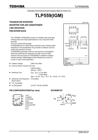
- 1. TLP559(IGM) 2002-05-271 TOSHIBA PHOTOCOUPLER GaAlAs IRED & PHOTO IC TLP559(IGM) TRANSISTOR INVERTER INVERTER FOR AIR CONDITIONER LINE RECEIVER IPM INTERFACES The TOSHIBA TLP559(IGM) consists of a GaAlAs high-output light emitting diode and a high speed detector of one chip photo diode- transistor. This unit is 8-lead DIP package. TLP559(IGM) has no internal base connection,and a Faraday shield integrated on the photodetector chip provides an effective common mode noise transient immunity. TLP559(IGM) guarantees minimum and maximum of propagation delay time,switching time dispersion,and high common mode transient immunity.There for TLP559(IGM) is suitable for isolation interface between IPM(Intelligent Power Module) and control IC circuits in motor control application. l Isolation Voltage : 2500 Vrms (Min) l Common Mode Transient Immunity :±10kV/µs (Min) @VCM = 1500 V l Switching Time : tpHL , tpLH = 0.1µs (Min) = 0.8µs (Max) @IF = 10 mA , VCC = 15 V , RL = 20 kΩ , Ta = 25°C l Switching Time Dispersion : 0.7µs (Max) (|tpLH−tpHL|) l TTL Compatible l UL Recognized : UL1577, File No. E67349 PIN CONFIGURATION(Top view) 1:N.C. 2:ANODE 3:CATHODE 4:N.C. 5:EMITTER 6:COLLECTOR 7:N.C. 8:VCC SCHEMATIC SHIELD JEDEC ― EIAJ ― TOSHIBA 11−10C4 Weight: 0.54 g Unit: mm
- 2. TLP559(IGM) 2002-05-272 MAXIMUM RATINGS (Ta = 25°C) CHARACTERISTIC SYMBOL RATING UNIT Forward Current (Note 1) IF 25 mA Pulse Forward Current (Note 2) IFP 50 mA Peak Transient Forward Current (Note 3) IFPT 1 A Reverse Voltage VR 5 V LED Diode Power Dissipation (Note 4) PD 45 mW Output Current IO 8 mA Peak Output Current IOP 16 mA Output Voltage VO −0.5~20 V Supply Voltage VCC −0.5~30 V DETECTOR Output Power Dissipation (Note 5) PO 100 mW Operating Temperature Range Topr −55~100 °C Storage Temperature Range Tstg −55~125 °C Lead Solder Temperature(10s) (Note 6) Tsol 260 °C Isolation Voltage(AC,1min.,R.H.≤60%,Ta=25°C) (Note 7) BVS 2500 Vrms (Note 1) Derate 0.5mA above 70°C. (Note 2) 50% duty cycle,1ms pulse width. Derate –1.0mA/°C above 70°C. (Note 3) Pulse width PW≤1µs,300pps. (Note 4) Derate 0.9mW/°C above 70°C. (Note 5) Derate 2mW/°C above 70°C. (Note 6) Soldering portion of lead : up to 2mm from the body of the device. (Note 7) Device considerd a two terminal device : pins1,2,3 and 4 shorted together and pins5,6,7 and 8 shorted together. ELECTRICAL CHARACTERISTICS (Ta = 25℃℃℃℃) CHARACTERISTIC SYMBOL TEST CONDITION MIN. TYP. MAX. UNIT Forward Voltage VF IF = 16 mA ― 1.65 1.85 V Forward Voltage Temperature Coefficient ∆VF /∆Ta IF = 16 mA ― −2 ― mV /°C Reverse Current IR VR = 5 V ― ― 10 µA LED Capacitance between Terminal CT V = 0, f = 1 MHz ― 45 ― pF IOH (1) IF = 0 mA, VCC = VO = 5.5 V ― 3 500 nA IOH (2) IF = 0 mA, VCC = 30 V VO = 20 V ― ― 5 High Level Output Current IOH IF = 0 mA, VCC = 30 V VO = 20 V, Ta = 70°C ― ― 50 µA High Level Supply Voltage ICCH IF = 0 mA, VCC = 30 V ― 0.01 1 µA Supply Voltage VCC ICC = 0.01 mA 30 ― ― V DETECTOR Output Voltage VO IO = 0.5 mA 20 ― ― V
- 3. TLP559(IGM) 2002-05-273 COUPLED ELECTRICAL CHARACTERISTICS (Ta = 25℃℃℃℃) CHARACTERISTIC SYMBOL TEST CONDITION MIN. TYP. MAX. UNIT IF = 10 mA, VCC = 4.5 V VO = 0.4 V 25 35 75 Current Transfer Ratio IO / IF IF = 10 mA, VCC = 4.5 V VO = 0.4 V, Ta = −25~100°C 15 ― ― % Low Level Output Voltage VOL IF = 16 mA, VCC = 4.5 V IO = 2.4 mA ― ― 0.4 V ISOLATION CHARACTERISTICS (Ta = 25℃℃℃℃) CHARACTERISTIC SYMBOL TEST CONDITION MIN. TYP. MAX. UNIT Capacitance Input to Output CS V = 0, f = 1 MHz ― 0.8 ― pF Isolation Resistance RS R.H.≤60%, VS = 500 V 5×10 10 10 14 ― Ω AC , 1minute 2500 ― ― AC , 1second, in oil ― 5000 ― Vrms Isolation Voltage BVS DC , 1minute,in oil ― 5000 ― Vdc SWITCHING CHARACTERISTICS (Ta = 25℃、℃、℃、℃、VCC = 15 V) CHARACTERISTIC SYMBOL TEST CIR- CUIT TEST CONDITION MIN. TYP. MAX. UNIT IF = 10 mA, RL = 20 kΩ 0.1 0.45 0.8 IF = 10 mA, RL = 20 kΩ Ta = 0~85°C 0.1 0.45 0.9 Propagation Delay Time (H→L) Propagation Delay Time (L→H) tpHL tpLH IF = 10 mA, RL = 20 kΩ Ta = −25~100°C 0.1 0.45 1.0 µs IF = 10 mA, RL = 20 kΩ ― 0.15 0.7 IF = 10 mA, RL = 20 kΩ Ta = 0~85°C ― 0.25 0.8 Switching Time Dispersion between ON and OFF |tpLH−tpHL| 1 IF = 20 mA, RL = 20 kΩ Ta = −25~100°C ― 0.25 0.9 µs Common Mode Transient Immunity at Logic High Output (Note 8) CMH IF = 0 mA, VCM = 1500 Vp−p, RL = 20 kΩ 10000 15000 ― V /µs Common Mode Transient Immunity at Logic Low Output (Note 8) CML 2 IF =10 mA, VCM = 1500 Vp−p, RL = 20 kΩ −10000 −15000 ― V /µs (Note 8) CML is the maximum rate of fall of the common mode voltage that can be sustained with the output voltage in the logic low state(Vo<1V). CMH is the maximum rate of rise of the common mode voltage that can be sustained with the output voltage in the logic high state(Vo>4V). (Note 9) Maximum electrostatic discharge voltage for any pins : 100V(C=200pF,R=0)
- 4. TLP559(IGM) 2002-05-274 TEST CIRCUIT 1 : Switching time test circuit PULSE INPUT PW=100µ DUTY RATIO=1/10 IF MONITOR OUTPUT MONITOR TEST CIRCUIT 2 : Common mode noise immunity test circuit PULSE GENERATOR OUTPUT MONITOR 10mA )s(ft )V(1200 LCM )s(rt )V(1200 HCM m = m = 、
- 5. TLP559(IGM) 2002-05-275 · TOSHIBA is continually working to improve the quality and reliability of its products. Nevertheless, semiconductor devices in general can malfunction or fail due to their inherent electrical sensitivity and vulnerability to physical stress. It is the responsibility of the buyer, when utilizing TOSHIBA products, to comply with the standards of safety in making a safe design for the entire system, and to avoid situations in which a malfunction or failure of such TOSHIBA products could cause loss of human life, bodily injury or damage to property. In developing your designs, please ensure that TOSHIBA products are used within specified operating ranges as set forth in the most recent TOSHIBA products specifications. Also, please keep in mind the precautions and conditions set forth in the “Handling Guide for Semiconductor Devices,” or “TOSHIBA Semiconductor Reliability Handbook” etc.. · The TOSHIBA products listed in this document are intended for usage in general electronics applications (computer, personal equipment, office equipment, measuring equipment, industrial robotics, domestic appliances, etc.). These TOSHIBA products are neither intended nor warranted for usage in equipment that requires extraordinarily high quality and/or reliability or a malfunction or failure of which may cause loss of human life or bodily injury (“Unintended Usage”). Unintended Usage include atomic energy control instruments, airplane or spaceship instruments, transportation instruments, traffic signal instruments, combustion control instruments, medical instruments, all types of safety devices, etc.. Unintended Usage of TOSHIBA products listed in this document shall be made at the customer’s own risk. · Gallium arsenide (GaAs) is a substance used in the products described in this document. GaAs dust and fumes are toxic. Do not break, cut or pulverize the product, or use chemicals to dissolve them. When disposing of the products, follow the appropriate regulations. Do not dispose of the products with other industrial waste or with domestic garbage. · The products described in this document are subject to the foreign exchange and foreign trade laws. · The information contained herein is presented only as a guide for the applications of our products. No responsibility is assumed by TOSHIBA CORPORATION for any infringements of intellectual property or other rights of the third parties which may result from its use. No license is granted by implication or otherwise under any intellectual property or other rights of TOSHIBA CORPORATION or others. · The information contained herein is subject to change without notice. 000707EBC RESTRICTIONS ON PRODUCT USE