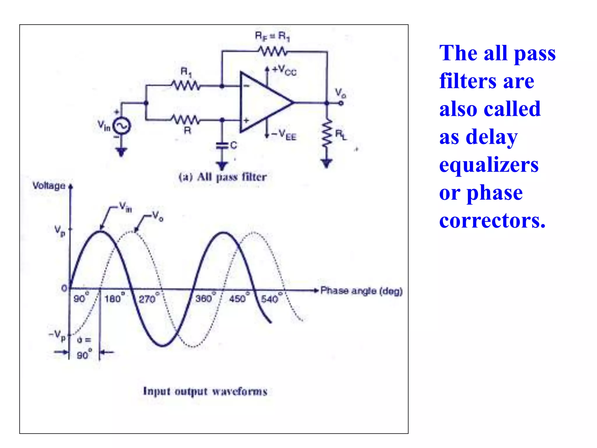
Downloaded 140 times
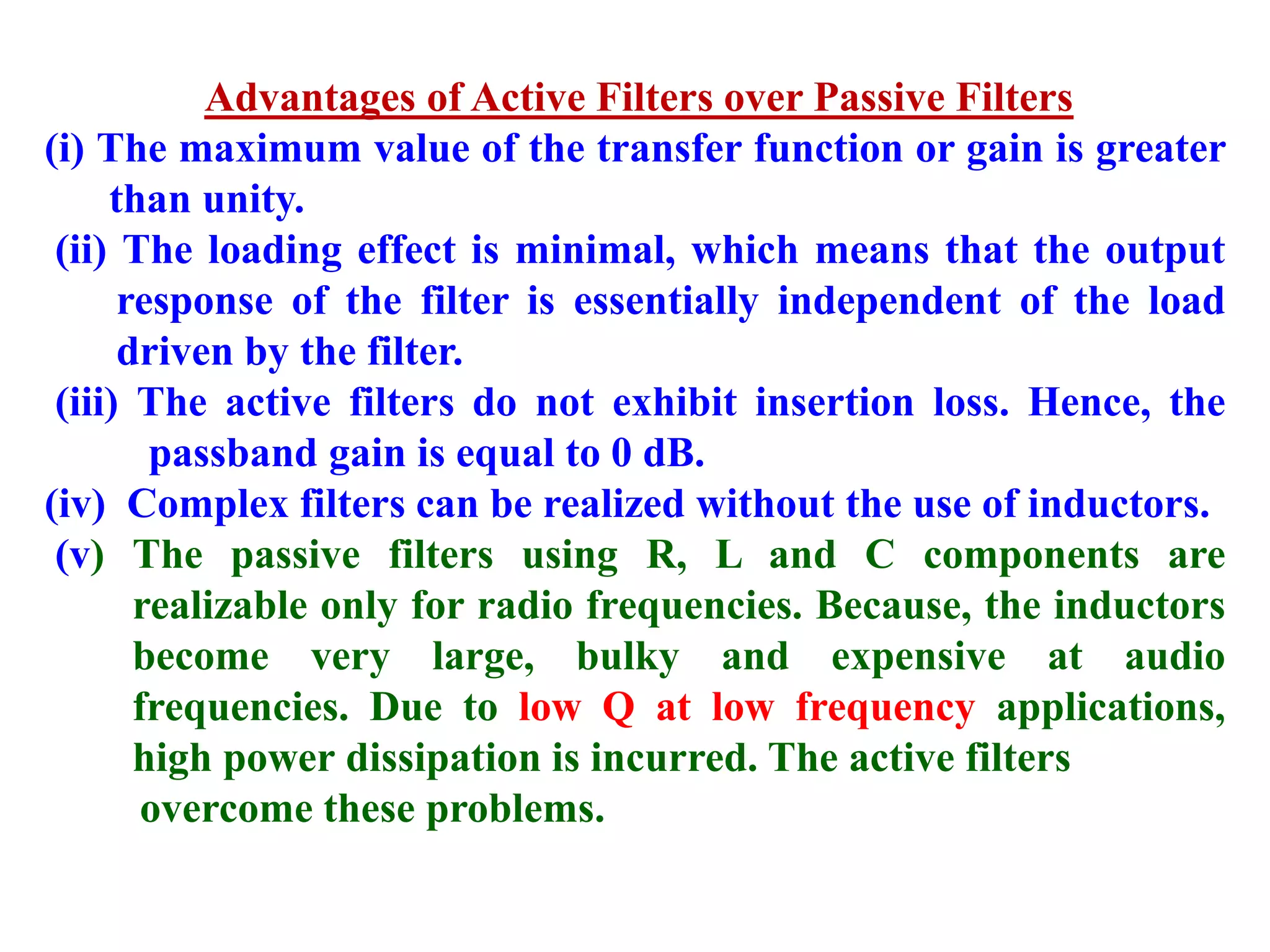
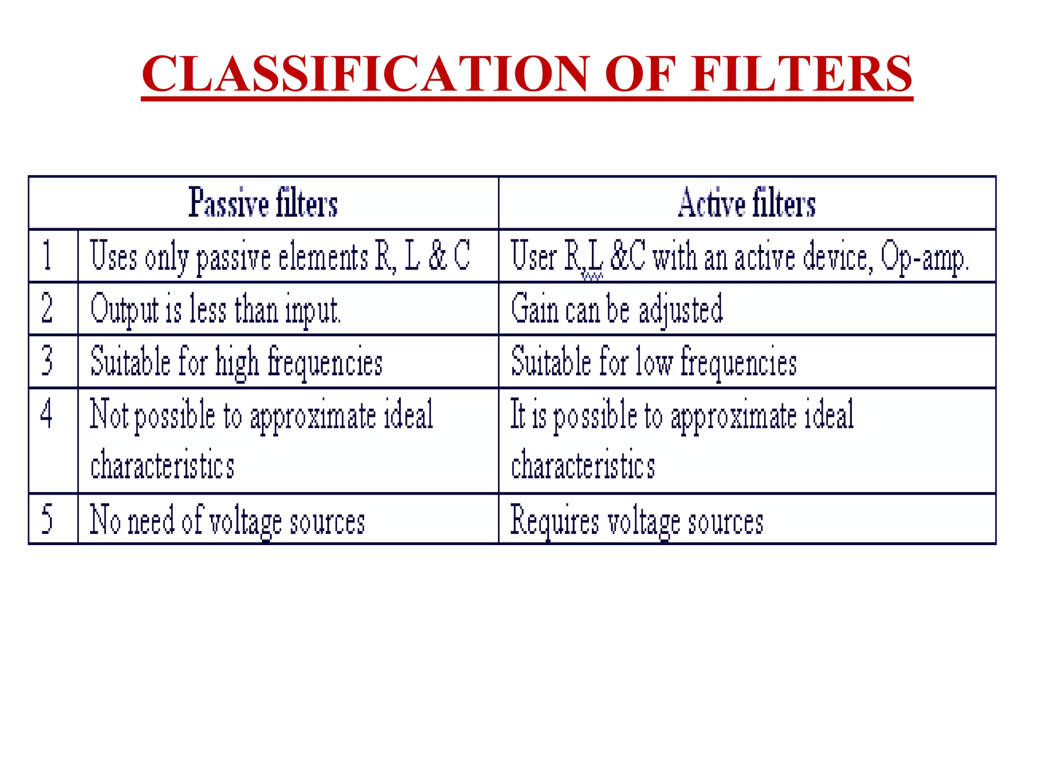
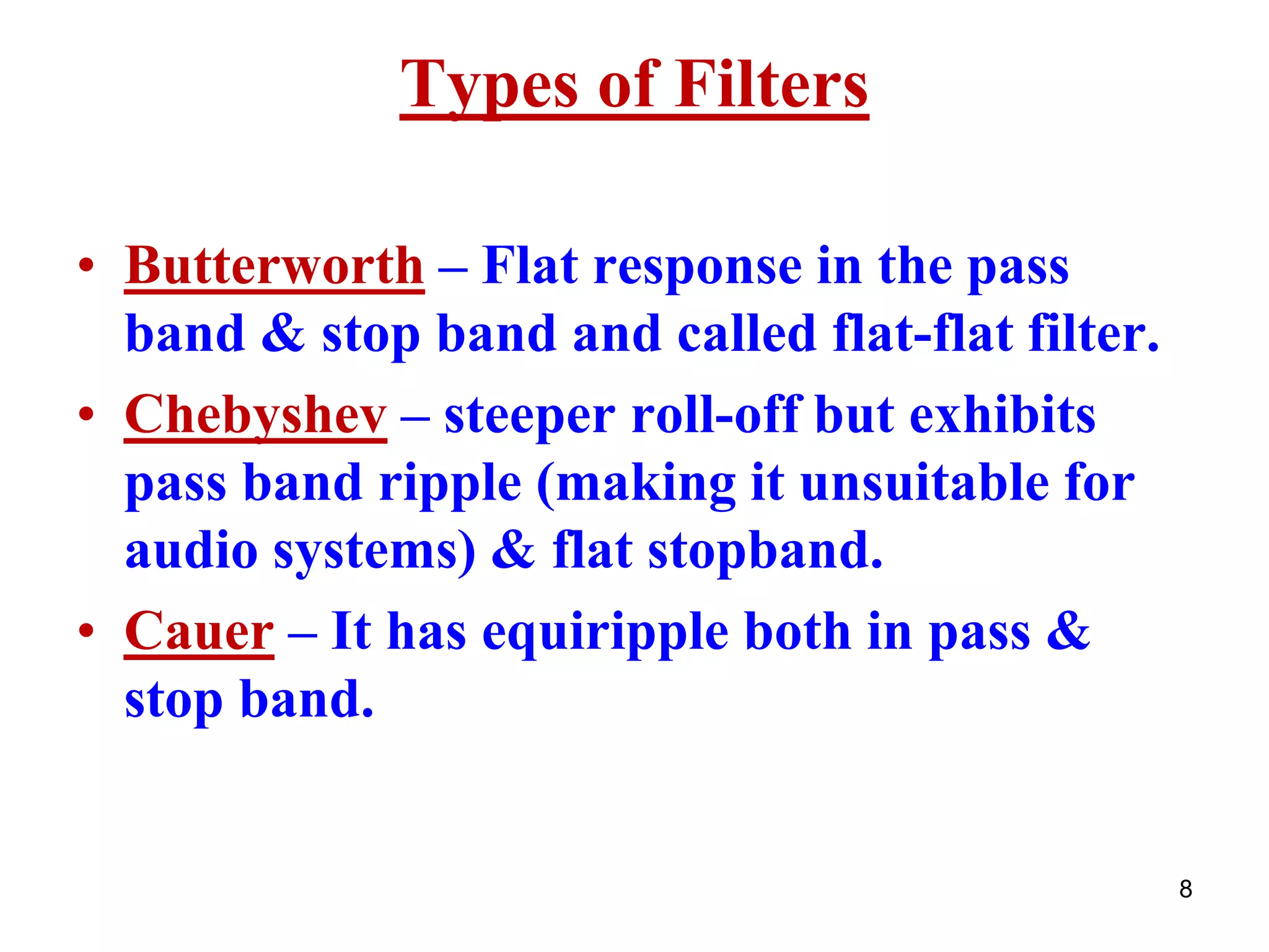
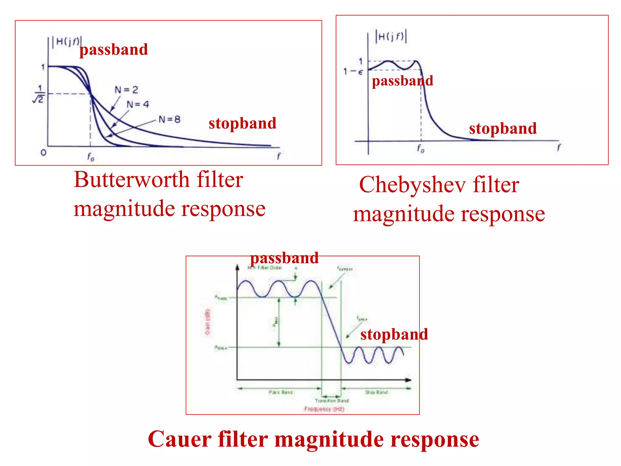
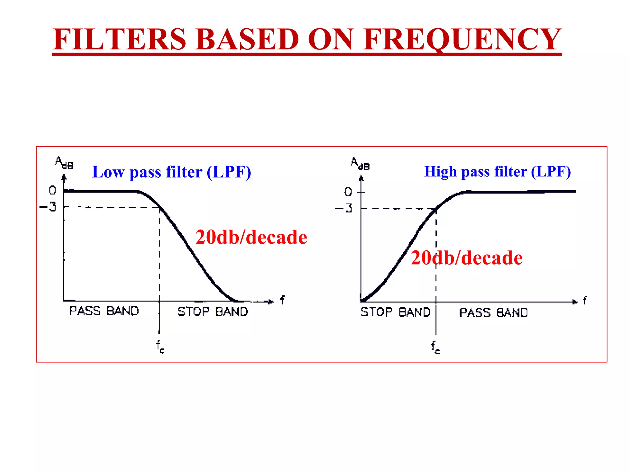
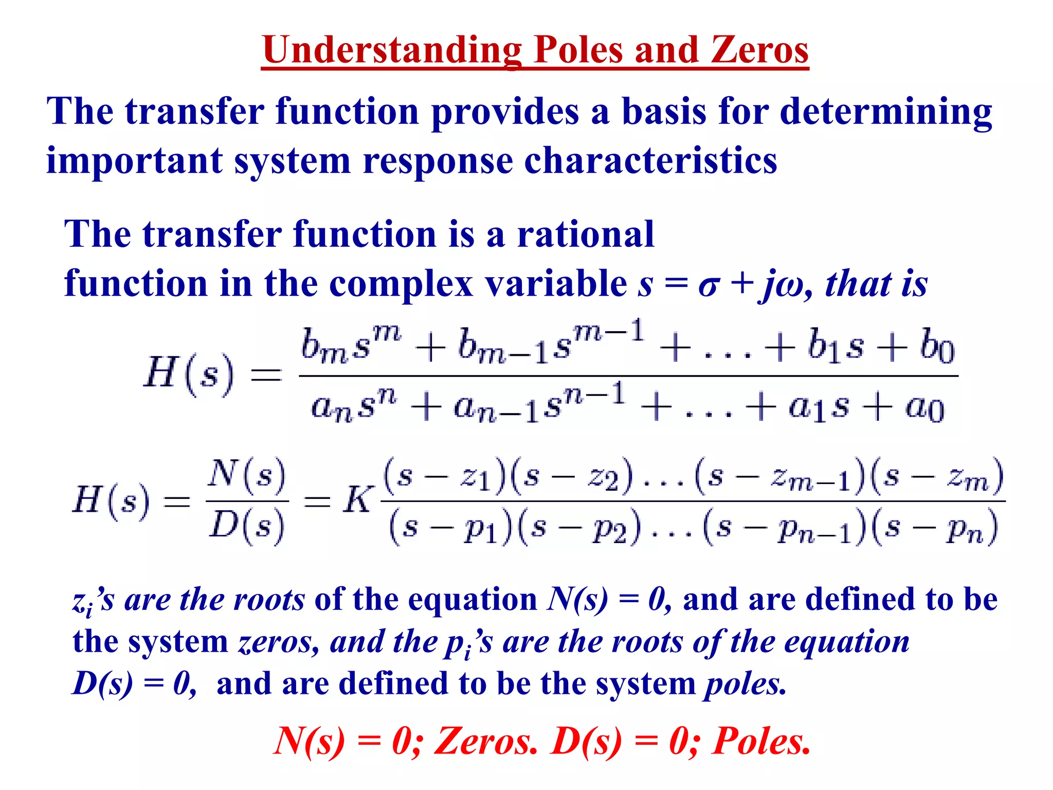
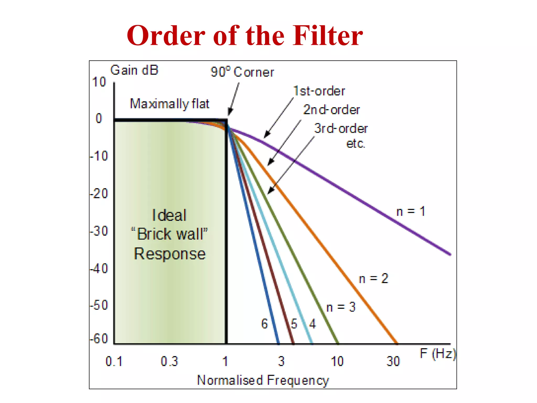
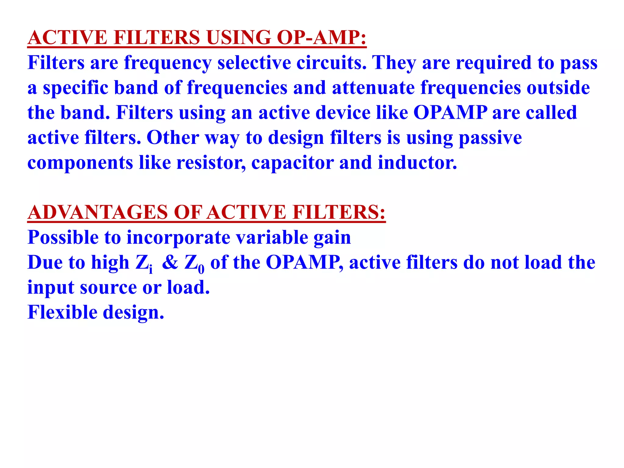
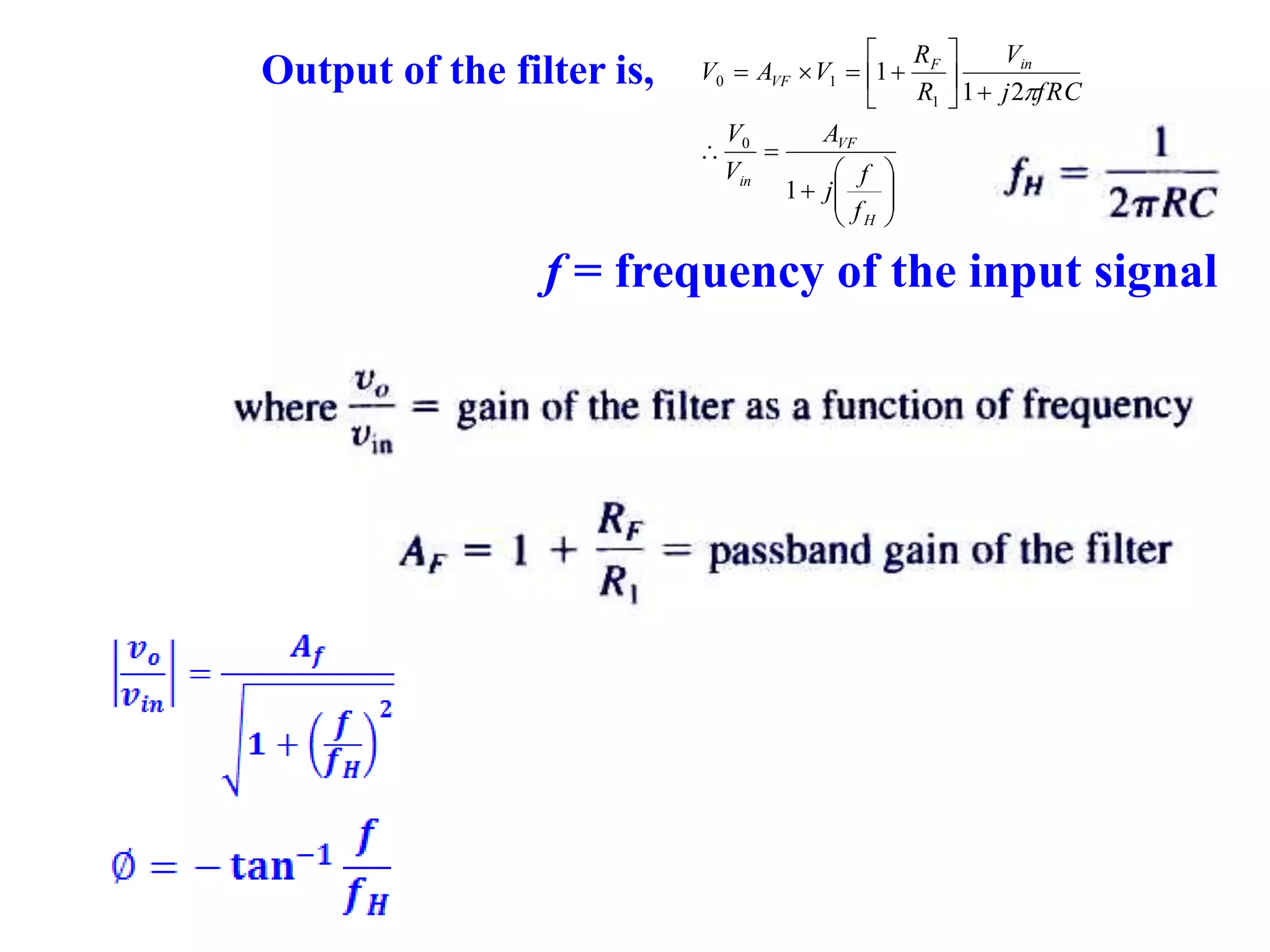
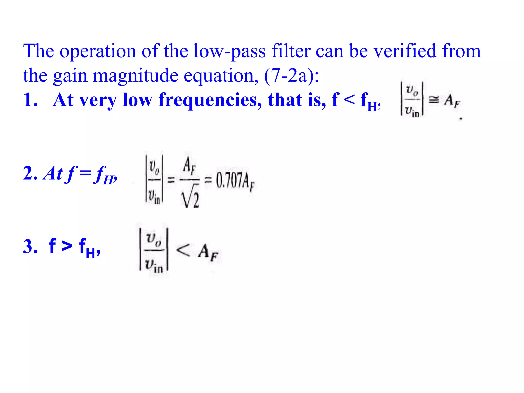
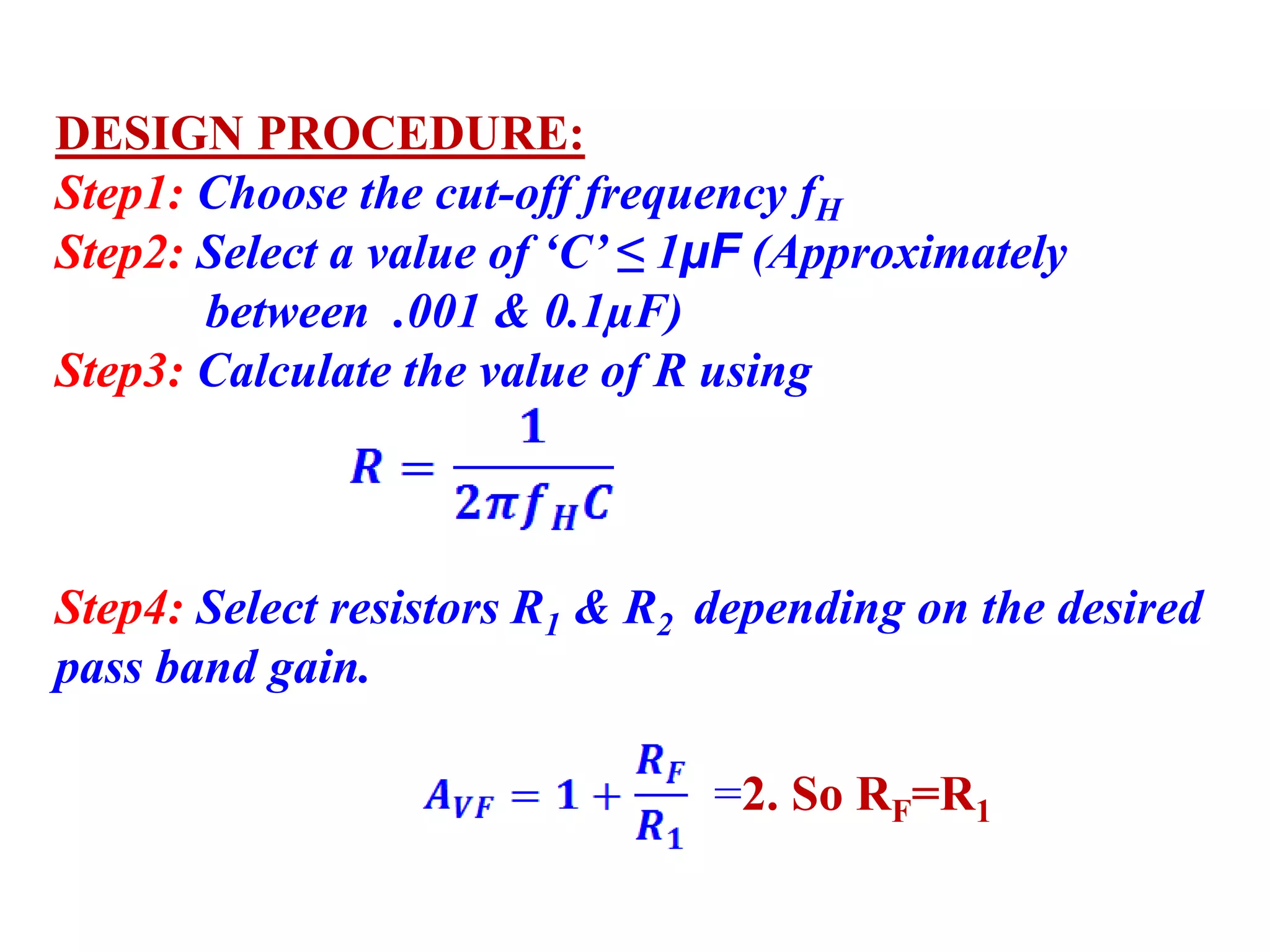
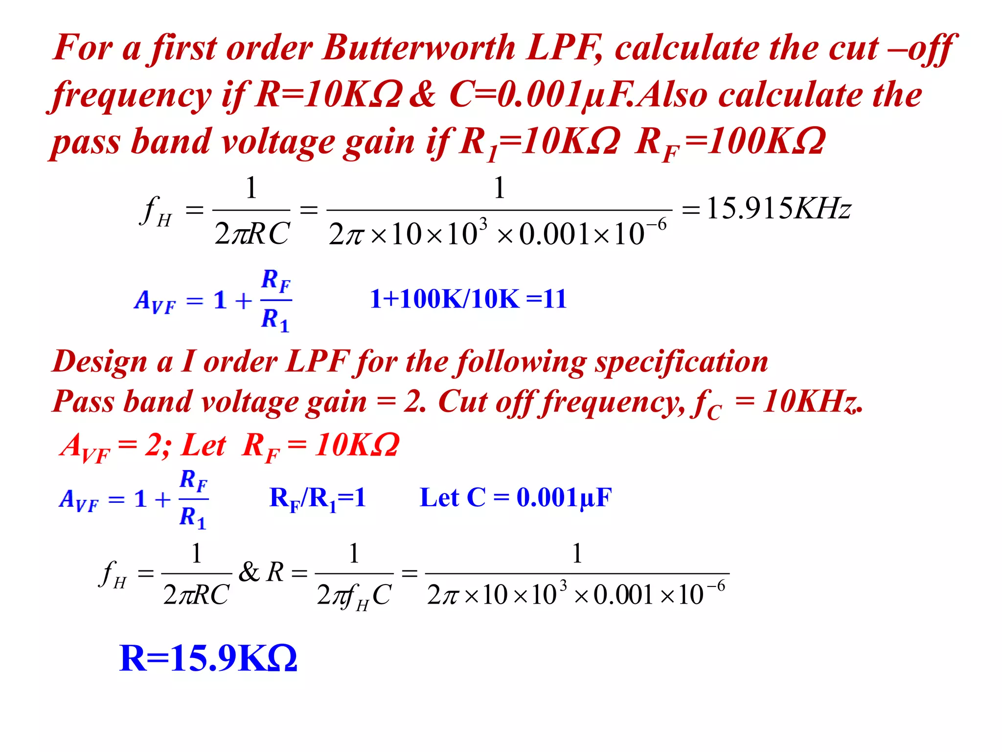
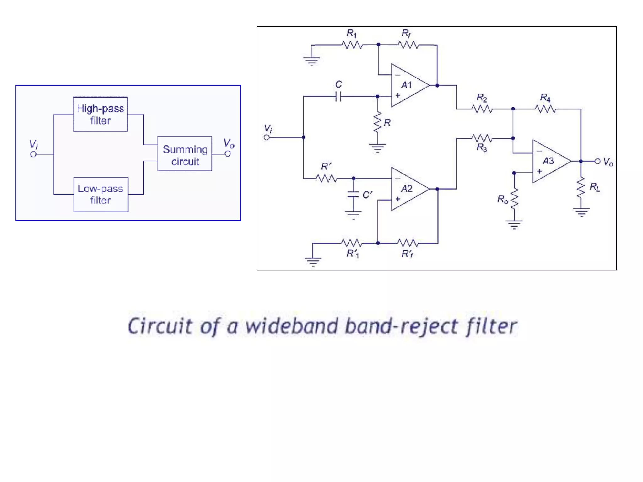
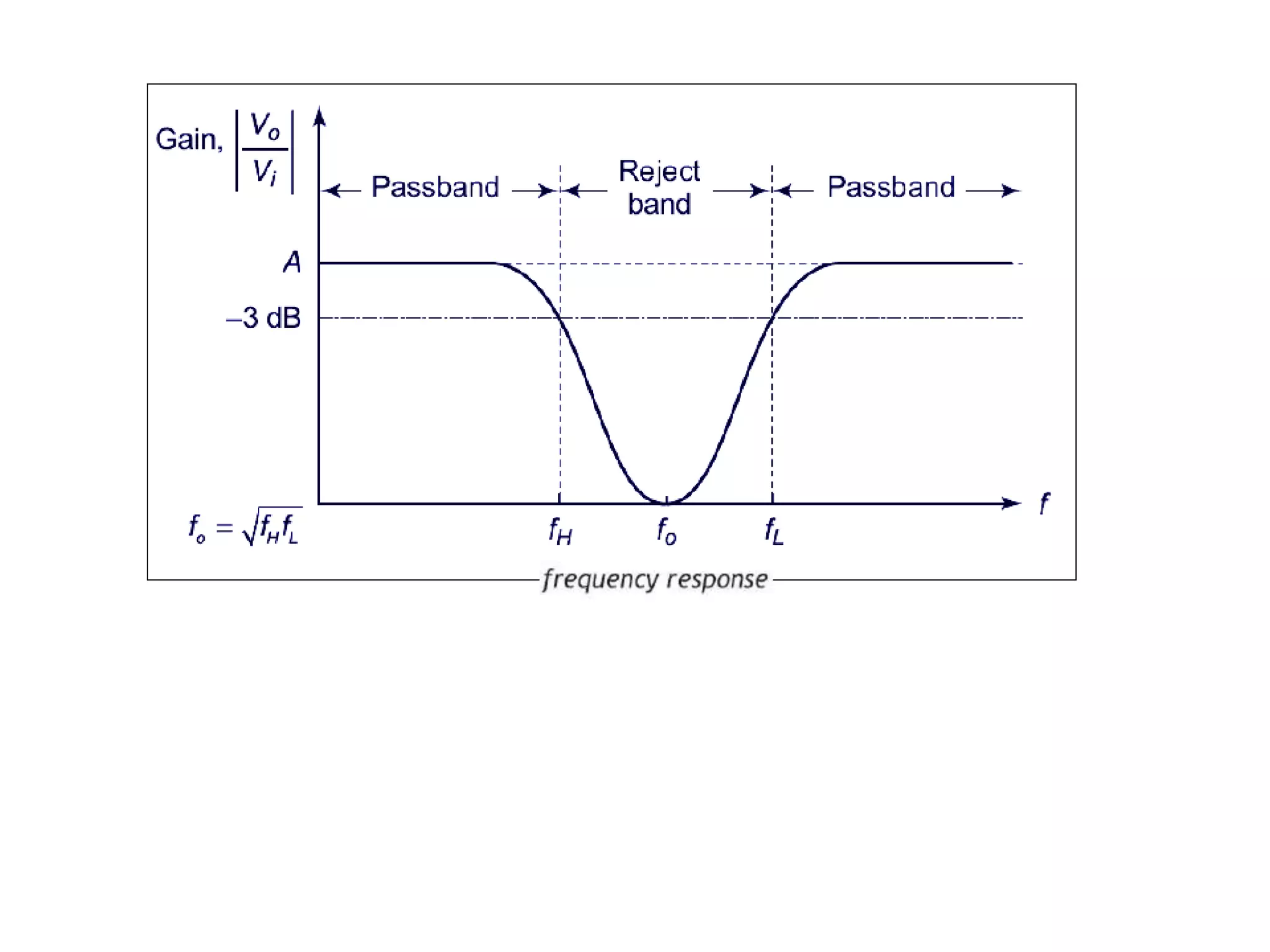
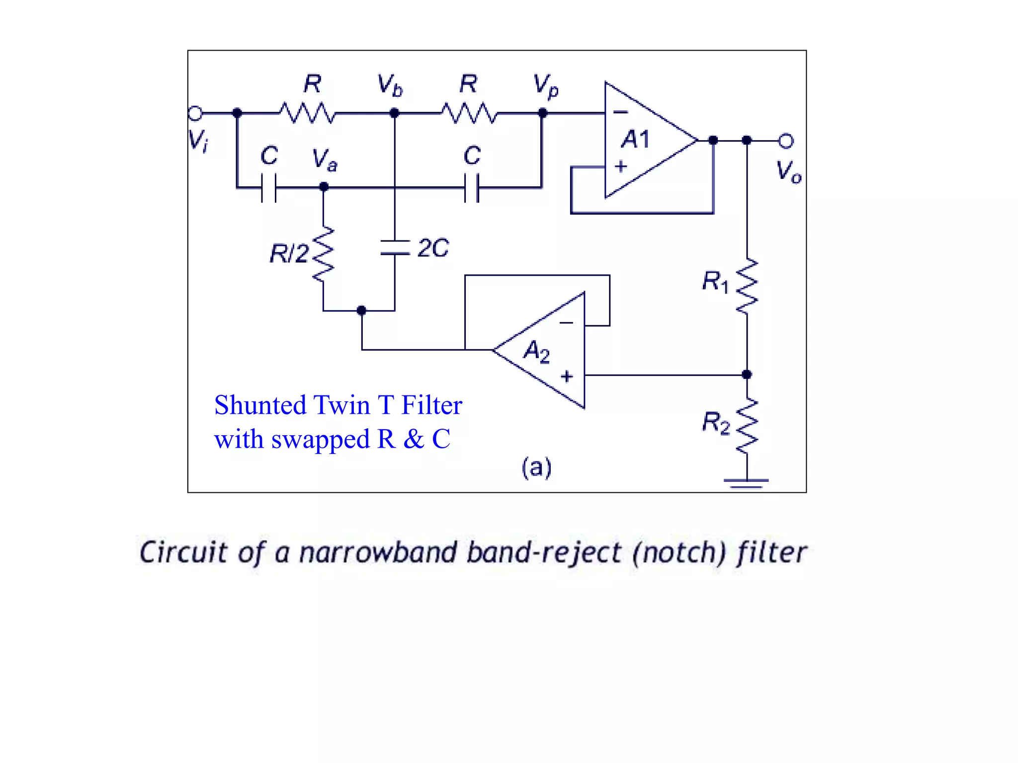
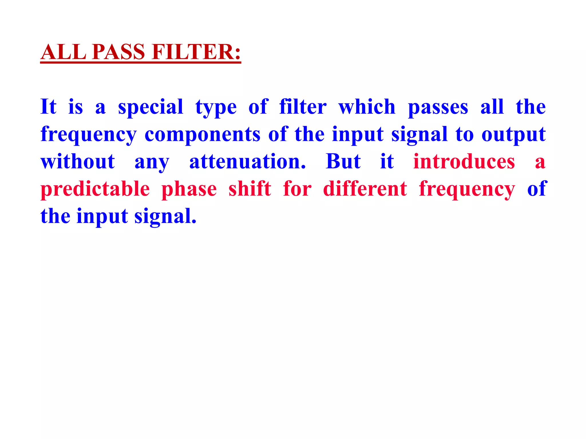
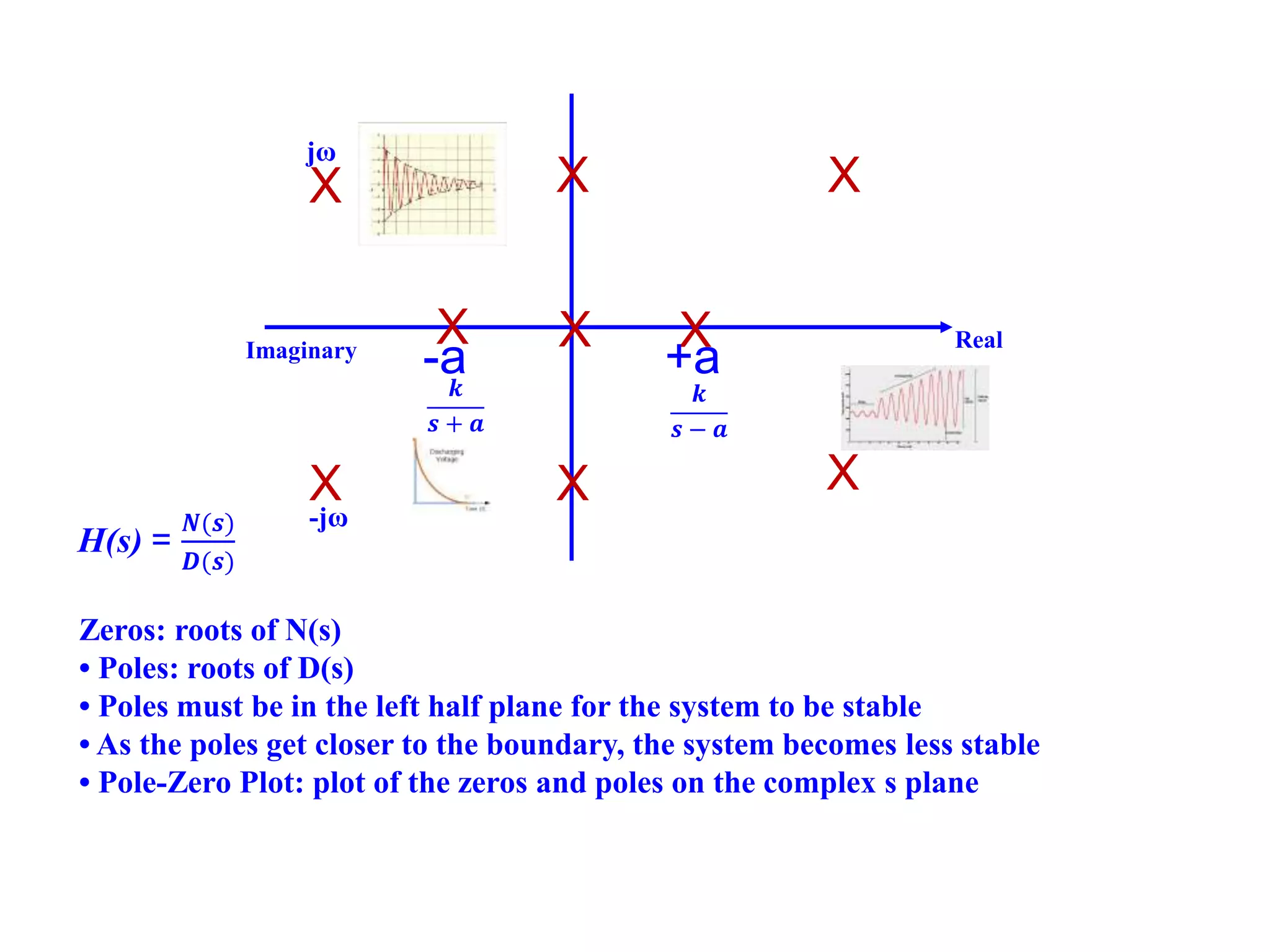

This document discusses active filters and provides information on different types of filters including: - Butterworth, Chebyshev, and Cauer filters and their magnitude responses. - Classification of filters as low pass, high pass, band pass and band reject based on their frequency responses. - Advantages of active filters over passive filters such as greater gain and flexibility in design. - Key concepts such as poles, zeros and order of filters and how they determine the frequency response. - Design procedures for first and second order low pass Butterworth filters using op-amps.


![Circuit Network Analysis - [Chapter5] Transfer function, frequency response, ...](https://cdn.slidesharecdn.com/ss_thumbnails/ch5-150613063859-lva1-app6891-thumbnail.jpg?width=640&height=640&fit=bounds)