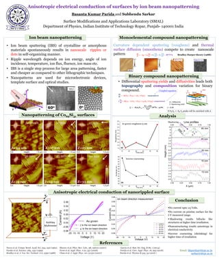
SlideShare a Scribd company logo
1 of 1
Cr
Anisotropic electrical conduction of surfaces by ion beam nanopatterning
Basanta Kumar Parida and Subhendu Sarkar
Surface Modifications and Applications Laboratory (SMAL)
Department of Physics, Indian Institute of Technology Ropar, Punjab- 140001 India
Ion beam nanopatterning Monoelemental compound nanopatterning
No current upto ±5 Volts.
No current on pristine surface for the
I-V measured range.
 Shadowing results hillocks like
structures at higher time irradiation.
Nanostructuring results anisotropy in
electrical conductivity.
Inverse coarsening (shrinking) for
higher time of irradiation
Email: bkparida@iitrpr.ac.in
sarkar@iitrpr.ac.in
• Ion beam sputtering (IBS) of crystalline or amorphous
materials spontaneously results in nanoscale ripples or
dots in self-organizing manner.
• Ripple wavelength depends on ion energy, angle of ion
incidence, temperature, ion flux, fluence, ion mass etc.
• IBS is a single step process for large area patterning, faster
and cheaper as compared to other lithographic techniques.
• Nanopatterns are used for microelectronic devices,
template surface and optical studies. • Differential sputtering yields and diffusivities leads both
topography and composition variation for binary
compound.
𝝏𝒉
𝝏𝒕
= −𝜴 𝑭 𝑨 + 𝜵. 𝑱 𝑨 + 𝑭 𝑩 + 𝜵. 𝑱 𝑩 𝐭𝐨𝐩𝐨𝐠𝐫𝐚𝐩𝐡𝐢𝐜𝐚𝐥
∆
𝝏𝒄 𝒔
𝝏𝒕
= 𝛀 𝒄 𝒃 − 𝟏 𝑭 𝑨 + 𝜵. 𝑱 𝑨 + 𝒄 𝒃 𝑭 𝑩 + 𝜵. 𝑱 𝑩 𝐜𝐨𝐦𝐩𝐨𝐬𝐢𝐭𝐢𝐨𝐧𝐚𝐥
𝑱𝒊 = −𝑫𝒊 𝒏 𝒔 𝜵𝑐 𝑠 𝒊 +
𝑫𝒊 𝑐 𝑠 𝒊 𝒏𝜴𝜸
𝒌 𝑩 𝑻
𝜵𝜵 𝟐 𝐡 − 𝝁𝒊 𝜵𝒉 , 𝐢 = 𝐀, 𝐁
Coupled equation
If 𝐷𝐴 𝑌𝐵 < 𝐷 𝐵 𝑌𝐴 peaks will be enriched with A
A
Binary
Monoelemental
B
Curvature dependent sputtering (roughens) and thermal
surface diffusion (smoothens) compete to create nanoscale
pattern
800 eV Ar+ → Cu 2000 eV Ar+ → Au
-20 -15 -10 -5 0 5 10 15 20
-0.08
-0.06
-0.04
-0.02
0.00
0.02
0.04
0.06
0.08
Current(A)
Voltage (V)
pristine
10 min
15 min
30 min
45 min
60 min
ion beam direction measurement
10 20 30 40 50 60
1.5
2.0
2.5
3.0
3.5
4.0
4.5
5.0
5.5
6.0
Roughness(nm)
Time (min)
(a)
10 20 30 40 50 60
34
36
38
40
42
44
46
48
50
52
54
56
(b)
Wavelength(nm)
Time (min)
Z=17 nm Z=13 nm
Z=19 nm Z=13 nm Z=35 nm
Z=40 nm
Z
As grown 10 min
30 min 45 min
15 min
60 min
Nanopatterning of Co69Si31 surfaces Analysis
0.00 0.25 0.50 0.75 1.00
-3.8
0.0
3.8
7.6
-1.7
0.0
1.7
3.4
-3.3
0.0
3.3
6.6
-1.5
0.0
1.5
3.0
-9
0
9
18
0.00 0.25 0.50 0.75 1.00
60 min
45 min
30 min
15 min
10 min
X (µm)
slope


Height(nm)
Line profiles
h
As grown roughness-5 nm
Inverse coarsening
Shadowing
Anisotropic electrical conduction of nanorippled surface
Conclusion
References
Navez et al. Compt. Rend. Acad. Sci. 254, 240 (1962) Shenoy et.al. Phys. Rev. Lett., 98, 256101 (2007) Garcia et al. Mat. Sci. Eng. R 86, 1 (2014)
Facsko et al. Science. 285, 1551 (1999) Frost et al. Appl. Phys. A 91, 551 (2008) Parida et al. Curr. Appl. Phys. 18, 993 (2018)
Bradley et al. J. Vac. Sci. Technol. A 6, 2390 (1988) Chan et al. J. Appl. Phys. 101 121301 (2007) Parida et al. Physica B 545, 34 (2018 )
Binary compound nanopatterning
𝝏𝒉
𝝏𝒕
= −𝒗 𝟎 + 𝜸 𝒙
𝝏𝒉
𝝏𝒙
+ 𝝑 𝒙
𝝏 𝟐 𝒉
𝝏𝒙 𝟐 + 𝝑 𝒚
𝝏 𝟐 𝒉
𝝏𝒚 𝟐 − 𝑩𝛁 𝟐
𝛁 𝟐
𝒉 Bradley-Harper theory (1988)
𝐷= Diffusivity
𝑌=Sputtering yield

More Related Content

What's hot

Low energy ion beam nanopatterning of Co_(x)Si_(1-x) surfaces
Low energy ion beam nanopatterning of Co_(x)Si_(1-x) surfacesLow energy ion beam nanopatterning of Co_(x)Si_(1-x) surfaces
Low energy ion beam nanopatterning of Co_(x)Si_(1-x) surfacesDr. Basanta Kumar Parida
 
mems module-4.pdf
mems module-4.pdfmems module-4.pdf
mems module-4.pdfjuby5
 
Ferroelectric nanostructures and their processing issues
Ferroelectric nanostructures and their processing issuesFerroelectric nanostructures and their processing issues
Ferroelectric nanostructures and their processing issues♪♫•*¨ *•.¸¸
 
Young Scientist Award in JPS (invited talk)
Young Scientist Award in JPS (invited talk)Young Scientist Award in JPS (invited talk)
Young Scientist Award in JPS (invited talk)Alto Osada
 
To show that the intensity of the radiation on the surface is inversely propo...
To show that the intensity of the radiation on the surface is inversely propo...To show that the intensity of the radiation on the surface is inversely propo...
To show that the intensity of the radiation on the surface is inversely propo...Salman Jailani
 
Prospects for Electron-Ion-Circuit Hybrid Quantum Systems_AltoOsada
Prospects for Electron-Ion-Circuit Hybrid Quantum Systems_AltoOsadaProspects for Electron-Ion-Circuit Hybrid Quantum Systems_AltoOsada
Prospects for Electron-Ion-Circuit Hybrid Quantum Systems_AltoOsadaAlto Osada
 
Application of electroceramics
Application of electroceramicsApplication of electroceramics
Application of electroceramicsSudhir Kumar
 
illustration of XRF and TEY STXM for image single particle
illustration of XRF and TEY STXM for image single particleillustration of XRF and TEY STXM for image single particle
illustration of XRF and TEY STXM for image single particleJigang Zhou
 
Joe Kelleher Presentation (May 27th 2014)
Joe Kelleher Presentation (May 27th 2014)Joe Kelleher Presentation (May 27th 2014)
Joe Kelleher Presentation (May 27th 2014)Roadshow2014
 
APS march meeting 2015
APS march meeting 2015APS march meeting 2015
APS march meeting 2015Po-Chun Yeh
 
Swift Heavy Ion Irradiation
Swift Heavy Ion IrradiationSwift Heavy Ion Irradiation
Swift Heavy Ion Irradiationkrishslide
 
Development of vibration and shock sensor using PZT ceramics
Development of vibration and shock sensor using PZT ceramicsDevelopment of vibration and shock sensor using PZT ceramics
Development of vibration and shock sensor using PZT ceramicsTharakamaheshDesilva
 
Sputtering in vacuum
Sputtering in vacuumSputtering in vacuum
Sputtering in vacuumMirza Baig
 
Graphene electronic properties (1)
Graphene electronic properties (1)Graphene electronic properties (1)
Graphene electronic properties (1)Sapan Anand
 
FSM roughness metrology for diffusers and very rough surfaces phot west 17 b
FSM roughness metrology for diffusers and very rough surfaces phot west 17 bFSM roughness metrology for diffusers and very rough surfaces phot west 17 b
FSM roughness metrology for diffusers and very rough surfaces phot west 17 bWojtek Walecki
 

What's hot (20)

presentation
presentationpresentation
presentation
 
Low energy ion beam nanopatterning of Co_(x)Si_(1-x) surfaces
Low energy ion beam nanopatterning of Co_(x)Si_(1-x) surfacesLow energy ion beam nanopatterning of Co_(x)Si_(1-x) surfaces
Low energy ion beam nanopatterning of Co_(x)Si_(1-x) surfaces
 
mems module-4.pdf
mems module-4.pdfmems module-4.pdf
mems module-4.pdf
 
TUDORTMUND1
TUDORTMUND1TUDORTMUND1
TUDORTMUND1
 
Neutronpdf
NeutronpdfNeutronpdf
Neutronpdf
 
Ferroelectric nanostructures and their processing issues
Ferroelectric nanostructures and their processing issuesFerroelectric nanostructures and their processing issues
Ferroelectric nanostructures and their processing issues
 
Young Scientist Award in JPS (invited talk)
Young Scientist Award in JPS (invited talk)Young Scientist Award in JPS (invited talk)
Young Scientist Award in JPS (invited talk)
 
To show that the intensity of the radiation on the surface is inversely propo...
To show that the intensity of the radiation on the surface is inversely propo...To show that the intensity of the radiation on the surface is inversely propo...
To show that the intensity of the radiation on the surface is inversely propo...
 
Prospects for Electron-Ion-Circuit Hybrid Quantum Systems_AltoOsada
Prospects for Electron-Ion-Circuit Hybrid Quantum Systems_AltoOsadaProspects for Electron-Ion-Circuit Hybrid Quantum Systems_AltoOsada
Prospects for Electron-Ion-Circuit Hybrid Quantum Systems_AltoOsada
 
Application of electroceramics
Application of electroceramicsApplication of electroceramics
Application of electroceramics
 
illustration of XRF and TEY STXM for image single particle
illustration of XRF and TEY STXM for image single particleillustration of XRF and TEY STXM for image single particle
illustration of XRF and TEY STXM for image single particle
 
Joe Kelleher Presentation (May 27th 2014)
Joe Kelleher Presentation (May 27th 2014)Joe Kelleher Presentation (May 27th 2014)
Joe Kelleher Presentation (May 27th 2014)
 
APS march meeting 2015
APS march meeting 2015APS march meeting 2015
APS march meeting 2015
 
Swift Heavy Ion Irradiation
Swift Heavy Ion IrradiationSwift Heavy Ion Irradiation
Swift Heavy Ion Irradiation
 
Development of vibration and shock sensor using PZT ceramics
Development of vibration and shock sensor using PZT ceramicsDevelopment of vibration and shock sensor using PZT ceramics
Development of vibration and shock sensor using PZT ceramics
 
Friction Force and its Relationship to the Electrostatic Charges at Interfaces.
Friction Force and its Relationship to the Electrostatic Charges at Interfaces.Friction Force and its Relationship to the Electrostatic Charges at Interfaces.
Friction Force and its Relationship to the Electrostatic Charges at Interfaces.
 
Sputtering in vacuum
Sputtering in vacuumSputtering in vacuum
Sputtering in vacuum
 
Graphene electronic properties (1)
Graphene electronic properties (1)Graphene electronic properties (1)
Graphene electronic properties (1)
 
17 session 2 fey - example sensitivity analysis
17 session 2   fey - example sensitivity analysis17 session 2   fey - example sensitivity analysis
17 session 2 fey - example sensitivity analysis
 
FSM roughness metrology for diffusers and very rough surfaces phot west 17 b
FSM roughness metrology for diffusers and very rough surfaces phot west 17 bFSM roughness metrology for diffusers and very rough surfaces phot west 17 b
FSM roughness metrology for diffusers and very rough surfaces phot west 17 b
 

Similar to Nanoripples for anisotropic electrical conduction

A few Curious Aspects of ZnO Nanostructures - Prof.Joy Mitra
A few Curious Aspects of ZnO Nanostructures - Prof.Joy MitraA few Curious Aspects of ZnO Nanostructures - Prof.Joy Mitra
A few Curious Aspects of ZnO Nanostructures - Prof.Joy MitraSTS FORUM 2016
 
Introduction to nanoscience and nanotechnology
Introduction to nanoscience and nanotechnologyIntroduction to nanoscience and nanotechnology
Introduction to nanoscience and nanotechnologyaimanmukhtar1
 
poster New Mexico Consortium 2015
poster New Mexico Consortium 2015poster New Mexico Consortium 2015
poster New Mexico Consortium 2015Swayandipta Dey
 
Ldb Convergenze Parallele_sorba_01
Ldb Convergenze Parallele_sorba_01Ldb Convergenze Parallele_sorba_01
Ldb Convergenze Parallele_sorba_01laboratoridalbasso
 
Daniel adrien franco lespinasse - status of magnetron sputtered qwr
Daniel adrien franco lespinasse - status of magnetron sputtered qwrDaniel adrien franco lespinasse - status of magnetron sputtered qwr
Daniel adrien franco lespinasse - status of magnetron sputtered qwrthinfilmsworkshop
 
Sputtering yield and nanopattern formation study of BNSiO2 (Borosil) at eleva...
Sputtering yield and nanopattern formation study of BNSiO2 (Borosil) at eleva...Sputtering yield and nanopattern formation study of BNSiO2 (Borosil) at eleva...
Sputtering yield and nanopattern formation study of BNSiO2 (Borosil) at eleva...Dr. Basanta Kumar Parida
 
Rosa alejandra lukaszew tests of the gurenvich odel toward larger field gra...
Rosa alejandra lukaszew   tests of the gurenvich odel toward larger field gra...Rosa alejandra lukaszew   tests of the gurenvich odel toward larger field gra...
Rosa alejandra lukaszew tests of the gurenvich odel toward larger field gra...thinfilmsworkshop
 
High k dielectric passivation of in as avalanche photodiodes
High k dielectric passivation of in as avalanche photodiodesHigh k dielectric passivation of in as avalanche photodiodes
High k dielectric passivation of in as avalanche photodiodesIan Sandall
 
Introduction to Scanning Tunneling Microscopy
Introduction to Scanning Tunneling MicroscopyIntroduction to Scanning Tunneling Microscopy
Introduction to Scanning Tunneling Microscopynirupam12
 
Llobet et al APL 107 223501 (2015)
Llobet et al APL 107 223501 (2015)Llobet et al APL 107 223501 (2015)
Llobet et al APL 107 223501 (2015)Chen Wang
 
ION IMPLANTATION
ION IMPLANTATIONION IMPLANTATION
ION IMPLANTATIONAJAL A J
 
Contact Resistance of Graphene/Single-Walled Carbon Nanotube Thin Film Transi...
Contact Resistance of Graphene/Single-Walled Carbon Nanotube Thin Film Transi...Contact Resistance of Graphene/Single-Walled Carbon Nanotube Thin Film Transi...
Contact Resistance of Graphene/Single-Walled Carbon Nanotube Thin Film Transi...Ryan Kim
 
Ion Implantation UPS.pdf
Ion Implantation UPS.pdfIon Implantation UPS.pdf
Ion Implantation UPS.pdfssuser0e2fb9
 
Laser texturing and applications
Laser texturing and applicationsLaser texturing and applications
Laser texturing and applicationsSuresh Lal
 

Similar to Nanoripples for anisotropic electrical conduction (20)

262 presentation1
262 presentation1262 presentation1
262 presentation1
 
A few Curious Aspects of ZnO Nanostructures - Prof.Joy Mitra
A few Curious Aspects of ZnO Nanostructures - Prof.Joy MitraA few Curious Aspects of ZnO Nanostructures - Prof.Joy Mitra
A few Curious Aspects of ZnO Nanostructures - Prof.Joy Mitra
 
Introduction to nanoscience and nanotechnology
Introduction to nanoscience and nanotechnologyIntroduction to nanoscience and nanotechnology
Introduction to nanoscience and nanotechnology
 
poster New Mexico Consortium 2015
poster New Mexico Consortium 2015poster New Mexico Consortium 2015
poster New Mexico Consortium 2015
 
1512.07321
1512.073211512.07321
1512.07321
 
Ldb Convergenze Parallele_sorba_01
Ldb Convergenze Parallele_sorba_01Ldb Convergenze Parallele_sorba_01
Ldb Convergenze Parallele_sorba_01
 
Daniel adrien franco lespinasse - status of magnetron sputtered qwr
Daniel adrien franco lespinasse - status of magnetron sputtered qwrDaniel adrien franco lespinasse - status of magnetron sputtered qwr
Daniel adrien franco lespinasse - status of magnetron sputtered qwr
 
Sputtering yield and nanopattern formation study of BNSiO2 (Borosil) at eleva...
Sputtering yield and nanopattern formation study of BNSiO2 (Borosil) at eleva...Sputtering yield and nanopattern formation study of BNSiO2 (Borosil) at eleva...
Sputtering yield and nanopattern formation study of BNSiO2 (Borosil) at eleva...
 
Rosa alejandra lukaszew tests of the gurenvich odel toward larger field gra...
Rosa alejandra lukaszew   tests of the gurenvich odel toward larger field gra...Rosa alejandra lukaszew   tests of the gurenvich odel toward larger field gra...
Rosa alejandra lukaszew tests of the gurenvich odel toward larger field gra...
 
High k dielectric passivation of in as avalanche photodiodes
High k dielectric passivation of in as avalanche photodiodesHigh k dielectric passivation of in as avalanche photodiodes
High k dielectric passivation of in as avalanche photodiodes
 
Santosh_Kr_Yadav_RAIM08
Santosh_Kr_Yadav_RAIM08Santosh_Kr_Yadav_RAIM08
Santosh_Kr_Yadav_RAIM08
 
Introduction to Scanning Tunneling Microscopy
Introduction to Scanning Tunneling MicroscopyIntroduction to Scanning Tunneling Microscopy
Introduction to Scanning Tunneling Microscopy
 
Optical Antenna
Optical AntennaOptical Antenna
Optical Antenna
 
Ldb Convergenze Parallele_11
Ldb Convergenze Parallele_11Ldb Convergenze Parallele_11
Ldb Convergenze Parallele_11
 
Llobet et al APL 107 223501 (2015)
Llobet et al APL 107 223501 (2015)Llobet et al APL 107 223501 (2015)
Llobet et al APL 107 223501 (2015)
 
nbigagli_00393293223155
nbigagli_00393293223155nbigagli_00393293223155
nbigagli_00393293223155
 
ION IMPLANTATION
ION IMPLANTATIONION IMPLANTATION
ION IMPLANTATION
 
Contact Resistance of Graphene/Single-Walled Carbon Nanotube Thin Film Transi...
Contact Resistance of Graphene/Single-Walled Carbon Nanotube Thin Film Transi...Contact Resistance of Graphene/Single-Walled Carbon Nanotube Thin Film Transi...
Contact Resistance of Graphene/Single-Walled Carbon Nanotube Thin Film Transi...
 
Ion Implantation UPS.pdf
Ion Implantation UPS.pdfIon Implantation UPS.pdf
Ion Implantation UPS.pdf
 
Laser texturing and applications
Laser texturing and applicationsLaser texturing and applications
Laser texturing and applications
 

More from Dr. Basanta Kumar Parida

Ion induced nanopatterning of CoSI binary alloy surfaces
Ion induced nanopatterning of CoSI binary alloy surfacesIon induced nanopatterning of CoSI binary alloy surfaces
Ion induced nanopatterning of CoSI binary alloy surfacesDr. Basanta Kumar Parida
 
plasma in ion source and sputtering systems
plasma in ion source and sputtering systemsplasma in ion source and sputtering systems
plasma in ion source and sputtering systemsDr. Basanta Kumar Parida
 
Low energy ion beam nanopatterning of CoxSi1-x Surfaces -Thesis Defense seminar
Low energy ion beam nanopatterning of CoxSi1-x Surfaces  -Thesis Defense seminarLow energy ion beam nanopatterning of CoxSi1-x Surfaces  -Thesis Defense seminar
Low energy ion beam nanopatterning of CoxSi1-x Surfaces -Thesis Defense seminarDr. Basanta Kumar Parida
 
ion induced nanopatterning of binary compound
ion induced nanopatterning of binary compoundion induced nanopatterning of binary compound
ion induced nanopatterning of binary compoundDr. Basanta Kumar Parida
 
Ion beam nanostructuring of CoSi surfaces
Ion beam nanostructuring of CoSi surfaces Ion beam nanostructuring of CoSi surfaces
Ion beam nanostructuring of CoSi surfaces Dr. Basanta Kumar Parida
 
Ion beam sputtered nanorippling of binary mxtures
Ion beam sputtered nanorippling of binary mxtures Ion beam sputtered nanorippling of binary mxtures
Ion beam sputtered nanorippling of binary mxtures Dr. Basanta Kumar Parida
 

More from Dr. Basanta Kumar Parida (20)

Ion induced nanopatterning of CoSI binary alloy surfaces
Ion induced nanopatterning of CoSI binary alloy surfacesIon induced nanopatterning of CoSI binary alloy surfaces
Ion induced nanopatterning of CoSI binary alloy surfaces
 
plasma in ion source and sputtering systems
plasma in ion source and sputtering systemsplasma in ion source and sputtering systems
plasma in ion source and sputtering systems
 
magnetron sputtering deposition system
magnetron sputtering deposition systemmagnetron sputtering deposition system
magnetron sputtering deposition system
 
Ion beam nanopatterning of binary alloy
Ion beam nanopatterning of binary alloyIon beam nanopatterning of binary alloy
Ion beam nanopatterning of binary alloy
 
Odishara debaadebi
Odishara debaadebiOdishara debaadebi
Odishara debaadebi
 
Atoms and molecules
Atoms and moleculesAtoms and molecules
Atoms and molecules
 
what is science
what is sciencewhat is science
what is science
 
Low energy ion beam nanopatterning of CoxSi1-x Surfaces -Thesis Defense seminar
Low energy ion beam nanopatterning of CoxSi1-x Surfaces  -Thesis Defense seminarLow energy ion beam nanopatterning of CoxSi1-x Surfaces  -Thesis Defense seminar
Low energy ion beam nanopatterning of CoxSi1-x Surfaces -Thesis Defense seminar
 
ion induced nanopatterning of binary compound
ion induced nanopatterning of binary compoundion induced nanopatterning of binary compound
ion induced nanopatterning of binary compound
 
Strangeness in particle physics
Strangeness in particle physicsStrangeness in particle physics
Strangeness in particle physics
 
Aluminium smelter
Aluminium smelterAluminium smelter
Aluminium smelter
 
Aluminium smelter vedanta jharsuguda
Aluminium smelter  vedanta jharsugudaAluminium smelter  vedanta jharsuguda
Aluminium smelter vedanta jharsuguda
 
Ion beam nanostructuring of CoSi surfaces
Ion beam nanostructuring of CoSi surfaces Ion beam nanostructuring of CoSi surfaces
Ion beam nanostructuring of CoSi surfaces
 
Ion beam sputtered nanorippling of binary mxtures
Ion beam sputtered nanorippling of binary mxtures Ion beam sputtered nanorippling of binary mxtures
Ion beam sputtered nanorippling of binary mxtures
 
English_odia dictionary
English_odia dictionaryEnglish_odia dictionary
English_odia dictionary
 
Odia bhagabata13
Odia bhagabata13Odia bhagabata13
Odia bhagabata13
 
Odia bhagabata11
Odia bhagabata11Odia bhagabata11
Odia bhagabata11
 
Odia bhagabata9
Odia bhagabata9Odia bhagabata9
Odia bhagabata9
 
Odia bhagabata8
Odia bhagabata8Odia bhagabata8
Odia bhagabata8
 
Odia bhagabata7
Odia bhagabata7Odia bhagabata7
Odia bhagabata7
 

Recently uploaded

“Oh GOSH! Reflecting on Hackteria's Collaborative Practices in a Global Do-It...
“Oh GOSH! Reflecting on Hackteria's Collaborative Practices in a Global Do-It...“Oh GOSH! Reflecting on Hackteria's Collaborative Practices in a Global Do-It...
“Oh GOSH! Reflecting on Hackteria's Collaborative Practices in a Global Do-It...Marc Dusseiller Dusjagr
 
BASLIQ CURRENT LOOKBOOK LOOKBOOK(1) (1).pdf
BASLIQ CURRENT LOOKBOOK  LOOKBOOK(1) (1).pdfBASLIQ CURRENT LOOKBOOK  LOOKBOOK(1) (1).pdf
BASLIQ CURRENT LOOKBOOK LOOKBOOK(1) (1).pdfSoniaTolstoy
 
Call Girls in Dwarka Mor Delhi Contact Us 9654467111
Call Girls in Dwarka Mor Delhi Contact Us 9654467111Call Girls in Dwarka Mor Delhi Contact Us 9654467111
Call Girls in Dwarka Mor Delhi Contact Us 9654467111Sapana Sha
 
Mastering the Unannounced Regulatory Inspection
Mastering the Unannounced Regulatory InspectionMastering the Unannounced Regulatory Inspection
Mastering the Unannounced Regulatory InspectionSafetyChain Software
 
Solving Puzzles Benefits Everyone (English).pptx
Solving Puzzles Benefits Everyone (English).pptxSolving Puzzles Benefits Everyone (English).pptx
Solving Puzzles Benefits Everyone (English).pptxOH TEIK BIN
 
Organic Name Reactions for the students and aspirants of Chemistry12th.pptx
Organic Name Reactions  for the students and aspirants of Chemistry12th.pptxOrganic Name Reactions  for the students and aspirants of Chemistry12th.pptx
Organic Name Reactions for the students and aspirants of Chemistry12th.pptxVS Mahajan Coaching Centre
 
Software Engineering Methodologies (overview)
Software Engineering Methodologies (overview)Software Engineering Methodologies (overview)
Software Engineering Methodologies (overview)eniolaolutunde
 
Incoming and Outgoing Shipments in 1 STEP Using Odoo 17
Incoming and Outgoing Shipments in 1 STEP Using Odoo 17Incoming and Outgoing Shipments in 1 STEP Using Odoo 17
Incoming and Outgoing Shipments in 1 STEP Using Odoo 17Celine George
 
How to Make a Pirate ship Primary Education.pptx
How to Make a Pirate ship Primary Education.pptxHow to Make a Pirate ship Primary Education.pptx
How to Make a Pirate ship Primary Education.pptxmanuelaromero2013
 
Introduction to AI in Higher Education_draft.pptx
Introduction to AI in Higher Education_draft.pptxIntroduction to AI in Higher Education_draft.pptx
Introduction to AI in Higher Education_draft.pptxpboyjonauth
 
Painted Grey Ware.pptx, PGW Culture of India
Painted Grey Ware.pptx, PGW Culture of IndiaPainted Grey Ware.pptx, PGW Culture of India
Painted Grey Ware.pptx, PGW Culture of IndiaVirag Sontakke
 
ECONOMIC CONTEXT - LONG FORM TV DRAMA - PPT
ECONOMIC CONTEXT - LONG FORM TV DRAMA - PPTECONOMIC CONTEXT - LONG FORM TV DRAMA - PPT
ECONOMIC CONTEXT - LONG FORM TV DRAMA - PPTiammrhaywood
 
internship ppt on smartinternz platform as salesforce developer
internship ppt on smartinternz platform as salesforce developerinternship ppt on smartinternz platform as salesforce developer
internship ppt on smartinternz platform as salesforce developerunnathinaik
 
History Class XII Ch. 3 Kinship, Caste and Class (1).pptx
History Class XII Ch. 3 Kinship, Caste and Class (1).pptxHistory Class XII Ch. 3 Kinship, Caste and Class (1).pptx
History Class XII Ch. 3 Kinship, Caste and Class (1).pptxsocialsciencegdgrohi
 
A Critique of the Proposed National Education Policy Reform
A Critique of the Proposed National Education Policy ReformA Critique of the Proposed National Education Policy Reform
A Critique of the Proposed National Education Policy ReformChameera Dedduwage
 
Computed Fields and api Depends in the Odoo 17
Computed Fields and api Depends in the Odoo 17Computed Fields and api Depends in the Odoo 17
Computed Fields and api Depends in the Odoo 17Celine George
 
_Math 4-Q4 Week 5.pptx Steps in Collecting Data
_Math 4-Q4 Week 5.pptx Steps in Collecting Data_Math 4-Q4 Week 5.pptx Steps in Collecting Data
_Math 4-Q4 Week 5.pptx Steps in Collecting DataJhengPantaleon
 
Biting mechanism of poisonous snakes.pdf
Biting mechanism of poisonous snakes.pdfBiting mechanism of poisonous snakes.pdf
Biting mechanism of poisonous snakes.pdfadityarao40181
 

Recently uploaded (20)

“Oh GOSH! Reflecting on Hackteria's Collaborative Practices in a Global Do-It...
“Oh GOSH! Reflecting on Hackteria's Collaborative Practices in a Global Do-It...“Oh GOSH! Reflecting on Hackteria's Collaborative Practices in a Global Do-It...
“Oh GOSH! Reflecting on Hackteria's Collaborative Practices in a Global Do-It...
 
BASLIQ CURRENT LOOKBOOK LOOKBOOK(1) (1).pdf
BASLIQ CURRENT LOOKBOOK  LOOKBOOK(1) (1).pdfBASLIQ CURRENT LOOKBOOK  LOOKBOOK(1) (1).pdf
BASLIQ CURRENT LOOKBOOK LOOKBOOK(1) (1).pdf
 
Call Girls in Dwarka Mor Delhi Contact Us 9654467111
Call Girls in Dwarka Mor Delhi Contact Us 9654467111Call Girls in Dwarka Mor Delhi Contact Us 9654467111
Call Girls in Dwarka Mor Delhi Contact Us 9654467111
 
Mastering the Unannounced Regulatory Inspection
Mastering the Unannounced Regulatory InspectionMastering the Unannounced Regulatory Inspection
Mastering the Unannounced Regulatory Inspection
 
Solving Puzzles Benefits Everyone (English).pptx
Solving Puzzles Benefits Everyone (English).pptxSolving Puzzles Benefits Everyone (English).pptx
Solving Puzzles Benefits Everyone (English).pptx
 
Organic Name Reactions for the students and aspirants of Chemistry12th.pptx
Organic Name Reactions  for the students and aspirants of Chemistry12th.pptxOrganic Name Reactions  for the students and aspirants of Chemistry12th.pptx
Organic Name Reactions for the students and aspirants of Chemistry12th.pptx
 
Software Engineering Methodologies (overview)
Software Engineering Methodologies (overview)Software Engineering Methodologies (overview)
Software Engineering Methodologies (overview)
 
Incoming and Outgoing Shipments in 1 STEP Using Odoo 17
Incoming and Outgoing Shipments in 1 STEP Using Odoo 17Incoming and Outgoing Shipments in 1 STEP Using Odoo 17
Incoming and Outgoing Shipments in 1 STEP Using Odoo 17
 
How to Make a Pirate ship Primary Education.pptx
How to Make a Pirate ship Primary Education.pptxHow to Make a Pirate ship Primary Education.pptx
How to Make a Pirate ship Primary Education.pptx
 
Introduction to AI in Higher Education_draft.pptx
Introduction to AI in Higher Education_draft.pptxIntroduction to AI in Higher Education_draft.pptx
Introduction to AI in Higher Education_draft.pptx
 
Painted Grey Ware.pptx, PGW Culture of India
Painted Grey Ware.pptx, PGW Culture of IndiaPainted Grey Ware.pptx, PGW Culture of India
Painted Grey Ware.pptx, PGW Culture of India
 
ECONOMIC CONTEXT - LONG FORM TV DRAMA - PPT
ECONOMIC CONTEXT - LONG FORM TV DRAMA - PPTECONOMIC CONTEXT - LONG FORM TV DRAMA - PPT
ECONOMIC CONTEXT - LONG FORM TV DRAMA - PPT
 
internship ppt on smartinternz platform as salesforce developer
internship ppt on smartinternz platform as salesforce developerinternship ppt on smartinternz platform as salesforce developer
internship ppt on smartinternz platform as salesforce developer
 
TataKelola dan KamSiber Kecerdasan Buatan v022.pdf
TataKelola dan KamSiber Kecerdasan Buatan v022.pdfTataKelola dan KamSiber Kecerdasan Buatan v022.pdf
TataKelola dan KamSiber Kecerdasan Buatan v022.pdf
 
History Class XII Ch. 3 Kinship, Caste and Class (1).pptx
History Class XII Ch. 3 Kinship, Caste and Class (1).pptxHistory Class XII Ch. 3 Kinship, Caste and Class (1).pptx
History Class XII Ch. 3 Kinship, Caste and Class (1).pptx
 
Model Call Girl in Bikash Puri Delhi reach out to us at 🔝9953056974🔝
Model Call Girl in Bikash Puri  Delhi reach out to us at 🔝9953056974🔝Model Call Girl in Bikash Puri  Delhi reach out to us at 🔝9953056974🔝
Model Call Girl in Bikash Puri Delhi reach out to us at 🔝9953056974🔝
 
A Critique of the Proposed National Education Policy Reform
A Critique of the Proposed National Education Policy ReformA Critique of the Proposed National Education Policy Reform
A Critique of the Proposed National Education Policy Reform
 
Computed Fields and api Depends in the Odoo 17
Computed Fields and api Depends in the Odoo 17Computed Fields and api Depends in the Odoo 17
Computed Fields and api Depends in the Odoo 17
 
_Math 4-Q4 Week 5.pptx Steps in Collecting Data
_Math 4-Q4 Week 5.pptx Steps in Collecting Data_Math 4-Q4 Week 5.pptx Steps in Collecting Data
_Math 4-Q4 Week 5.pptx Steps in Collecting Data
 
Biting mechanism of poisonous snakes.pdf
Biting mechanism of poisonous snakes.pdfBiting mechanism of poisonous snakes.pdf
Biting mechanism of poisonous snakes.pdf
 

Nanoripples for anisotropic electrical conduction

  • 1. Cr Anisotropic electrical conduction of surfaces by ion beam nanopatterning Basanta Kumar Parida and Subhendu Sarkar Surface Modifications and Applications Laboratory (SMAL) Department of Physics, Indian Institute of Technology Ropar, Punjab- 140001 India Ion beam nanopatterning Monoelemental compound nanopatterning No current upto ±5 Volts. No current on pristine surface for the I-V measured range.  Shadowing results hillocks like structures at higher time irradiation. Nanostructuring results anisotropy in electrical conductivity. Inverse coarsening (shrinking) for higher time of irradiation Email: bkparida@iitrpr.ac.in sarkar@iitrpr.ac.in • Ion beam sputtering (IBS) of crystalline or amorphous materials spontaneously results in nanoscale ripples or dots in self-organizing manner. • Ripple wavelength depends on ion energy, angle of ion incidence, temperature, ion flux, fluence, ion mass etc. • IBS is a single step process for large area patterning, faster and cheaper as compared to other lithographic techniques. • Nanopatterns are used for microelectronic devices, template surface and optical studies. • Differential sputtering yields and diffusivities leads both topography and composition variation for binary compound. 𝝏𝒉 𝝏𝒕 = −𝜴 𝑭 𝑨 + 𝜵. 𝑱 𝑨 + 𝑭 𝑩 + 𝜵. 𝑱 𝑩 𝐭𝐨𝐩𝐨𝐠𝐫𝐚𝐩𝐡𝐢𝐜𝐚𝐥 ∆ 𝝏𝒄 𝒔 𝝏𝒕 = 𝛀 𝒄 𝒃 − 𝟏 𝑭 𝑨 + 𝜵. 𝑱 𝑨 + 𝒄 𝒃 𝑭 𝑩 + 𝜵. 𝑱 𝑩 𝐜𝐨𝐦𝐩𝐨𝐬𝐢𝐭𝐢𝐨𝐧𝐚𝐥 𝑱𝒊 = −𝑫𝒊 𝒏 𝒔 𝜵𝑐 𝑠 𝒊 + 𝑫𝒊 𝑐 𝑠 𝒊 𝒏𝜴𝜸 𝒌 𝑩 𝑻 𝜵𝜵 𝟐 𝐡 − 𝝁𝒊 𝜵𝒉 , 𝐢 = 𝐀, 𝐁 Coupled equation If 𝐷𝐴 𝑌𝐵 < 𝐷 𝐵 𝑌𝐴 peaks will be enriched with A A Binary Monoelemental B Curvature dependent sputtering (roughens) and thermal surface diffusion (smoothens) compete to create nanoscale pattern 800 eV Ar+ → Cu 2000 eV Ar+ → Au -20 -15 -10 -5 0 5 10 15 20 -0.08 -0.06 -0.04 -0.02 0.00 0.02 0.04 0.06 0.08 Current(A) Voltage (V) pristine 10 min 15 min 30 min 45 min 60 min ion beam direction measurement 10 20 30 40 50 60 1.5 2.0 2.5 3.0 3.5 4.0 4.5 5.0 5.5 6.0 Roughness(nm) Time (min) (a) 10 20 30 40 50 60 34 36 38 40 42 44 46 48 50 52 54 56 (b) Wavelength(nm) Time (min) Z=17 nm Z=13 nm Z=19 nm Z=13 nm Z=35 nm Z=40 nm Z As grown 10 min 30 min 45 min 15 min 60 min Nanopatterning of Co69Si31 surfaces Analysis 0.00 0.25 0.50 0.75 1.00 -3.8 0.0 3.8 7.6 -1.7 0.0 1.7 3.4 -3.3 0.0 3.3 6.6 -1.5 0.0 1.5 3.0 -9 0 9 18 0.00 0.25 0.50 0.75 1.00 60 min 45 min 30 min 15 min 10 min X (µm) slope   Height(nm) Line profiles h As grown roughness-5 nm Inverse coarsening Shadowing Anisotropic electrical conduction of nanorippled surface Conclusion References Navez et al. Compt. Rend. Acad. Sci. 254, 240 (1962) Shenoy et.al. Phys. Rev. Lett., 98, 256101 (2007) Garcia et al. Mat. Sci. Eng. R 86, 1 (2014) Facsko et al. Science. 285, 1551 (1999) Frost et al. Appl. Phys. A 91, 551 (2008) Parida et al. Curr. Appl. Phys. 18, 993 (2018) Bradley et al. J. Vac. Sci. Technol. A 6, 2390 (1988) Chan et al. J. Appl. Phys. 101 121301 (2007) Parida et al. Physica B 545, 34 (2018 ) Binary compound nanopatterning 𝝏𝒉 𝝏𝒕 = −𝒗 𝟎 + 𝜸 𝒙 𝝏𝒉 𝝏𝒙 + 𝝑 𝒙 𝝏 𝟐 𝒉 𝝏𝒙 𝟐 + 𝝑 𝒚 𝝏 𝟐 𝒉 𝝏𝒚 𝟐 − 𝑩𝛁 𝟐 𝛁 𝟐 𝒉 Bradley-Harper theory (1988) 𝐷= Diffusivity 𝑌=Sputtering yield