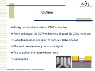
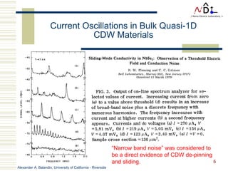
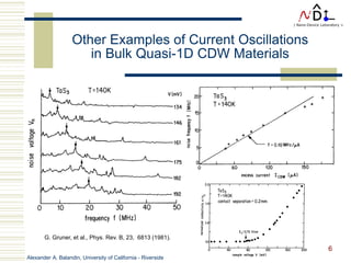
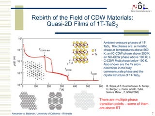
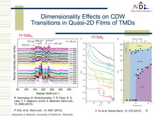
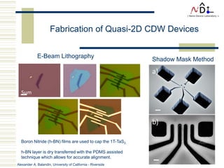
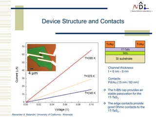
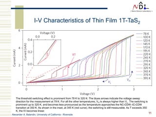
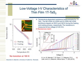
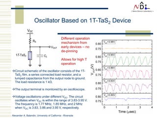
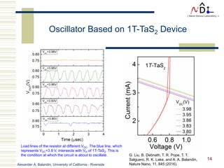
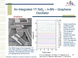
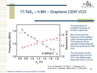
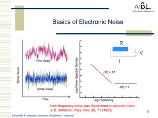
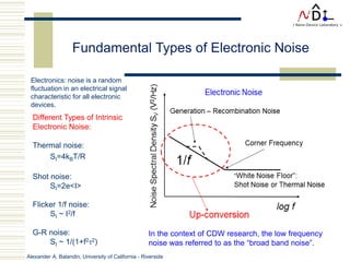
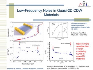
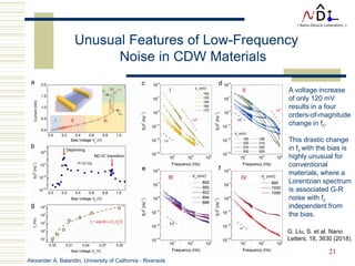
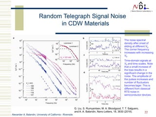
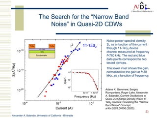
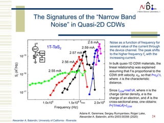
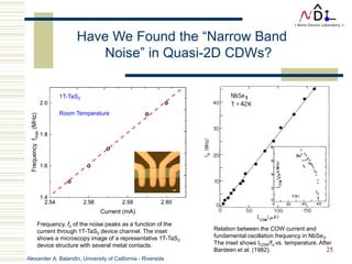
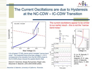
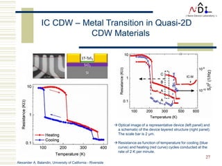
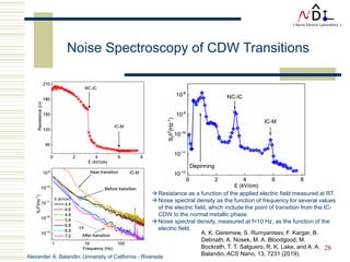
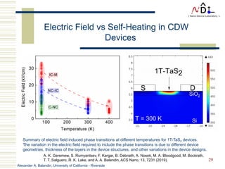
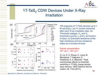
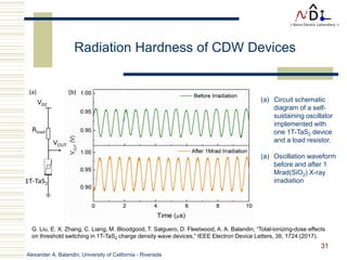
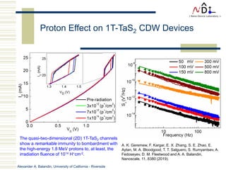
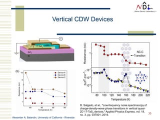
SlideShare a Scribd company logo
Alexander A. Balandin
Nano-Device Laboratory: NDL
Center for Phonon Optimized Engineered Materials: POEM
Department of Electrical and Computer Engineering
Materials Science and Engineering Program
University of California – Riverside
APS Spring – Colorado – 2020
Monitoring and Controlling Charge-
Density-Waves in 2D Materials
Alexander A. Balandin, University of California - Riverside
Background and motivations: CDW and noise
 From bulk quasi-1D CDW to thin films of quasi-2D CDW materials
Room temperature operation of quasi-2D CDW devices
Electronic low-frequency noise as a signal
The search for the “narrow band noise”
Conclusions
Outline
Alexander A. Balandin, University of California - Riverside
Charge Density Waves: Quasi-1D Crystals
R.V. Coleman, Phys. Rev. Lett.,
55, 394 (1985).
Macroscopic quantum
phenomena: coherence
length >1 µm
Quantum materials
Alexander A. Balandin, University of California - Riverside
4
 Electric-field-dependent
conductivity normalized
to RT conductivity.
 The inset shows typical
DC I-V characteristics of
the same material.
 CDW de-pinning was the
main mechanism for
device operation.
 One can get oscillations
at output with DC input.
The image is after G. Gruner, Rev.
Mod. Phys., 60, 1129 (1988).
Charge Density Waves: Early Devices
Alexander A. Balandin, University of California - Riverside
5
Current Oscillations in Bulk Quasi-1D
CDW Materials
“Narrow band noise” was considered to
be a direct evidence of CDW de-pinning
and sliding.
Alexander A. Balandin, University of California - Riverside
6
G. Gruner, et al., Phys. Rev. B, 23, 6813 (1981).
Other Examples of Current Oscillations
in Bulk Quasi-1D CDW Materials
Alexander A. Balandin, University of California - Riverside 7
Rebirth of the Field of CDW Materials:
Quasi-2D Films of 1T-TaS2
Ambient-pressure phases of 1T-
TaS2. The phases are: a metallic
phase at temperatures above 550
K; an IC-CDW phase above 350 K;
an NC-CDW phase above 190 K; a
C-CDW Mott phase below 190 K.
Also shown are the Ta atom
distortions in the fully
commensurate phase and the
crystal structure of 1T-TaS2.
B. Sipos, A.F. Kusmartseva, A. Akrap,
H. Berger, L. Forró, and E. Tutiš,
Nature Mater., 7, 960 (2008).
There are multiple phase
transition points – some of them
are above RT
Alexander A. Balandin, University of California - Riverside
8Y. Yu et al, Nature Nano, 10, 270 (2015)
Dimensionality Effects on CDW
Transitions in Quasi-2D Films of TMDs
R. Samnakay, D. Wickramaratne, T. R. Pope, R. K.
Lake, T. T. Salguero, and A. A. Balandin, Nano Lett.,
15, 2965 (2015).
P. Goli, et al., Nano Lett., 12, 5941 (2012).
1T-TaSe2 1T-TaS2
Alexander A. Balandin, University of California - Riverside
Fabrication of Quasi-2D CDW Devices
Boron Nitride (h-BN) films are used to cap the 1T-TaS2.
h-BN layer is dry transferred with the PDMS assisted
technique which allows for accurate alignment.
5μm
Shadow Mask Method
E-Beam Lithography
Alexander A. Balandin, University of California - Riverside
Device Structure and Contacts
 The h-BN cap provides air
stable passivation for the
1T-TaS2.
 The edge contacts provide
good Ohmic contacts to the
1T-TaS2.
Channel thickness:
t = 6 nm - 9 nm
Contacts:
Pd/Au (15 nm / 60 nm)
Alexander A. Balandin, University of California - Riverside
11
The threshold switching effect is prominent from 78 K to 320 K. The blues arrows indicate the voltage sweep
direction for the measurement at 78 K. For all the other temperatures, VH is always higher than VL. The switching is
prominent up to 320 K, and becomes less pronounced as the temperature approaches the NC-CDW–IC-CDW
transition at 350 K. As shown in the inset, at 345 K (red curve), the switching is still measurable. As T exceeds 350
K, the IV becomes linear.
I-V Characteristics of Thin Film 1T-TaS2
Alexander A. Balandin, University of California - Riverside
12
Low-Voltage I-V Characteristics of
Thin Film 1T-TaS2
 Temperature-dependent resistance measurements for 1T-
TaS2. The NC-CDW–IC-CDW and IC-CDW–NC-CDW
transitions happen at 350 K and 340 K during the heating
and cooling process, respectively. The resistance is
measured at low voltage (V=20 mV).
 Resistances match
No transition at 180 K
G. Liu, B. Debnath, T. R. Pope, T. T. Salguero, R. K.
Lake, and A. A. Balandin, Nature Nano, 11, 845 (2016).
Alexander A. Balandin, University of California - Riverside
13
Oscillator Based on 1T-TaS2 Device
Circuit schematic of the oscillator consists of the 1T-
TaS2 film, a series connected load resistor, and a
lumped capacitance from the output node to ground.
The load resistance is 1 kΩ.
The output terminal is monitored by an oscilloscope.
Voltage oscillations under different VDC. The circuit
oscillates when VDC is within the range of 3.83-3.95 V.
The frequency is 1.77 MHz, 1.85 MHz, and 2 MHz
when VDC is 3.83, 3.86 and 3.95 V, respectively.
Different operation
mechanism from
early devices – no
de-pinning
Allows for high T
operation
Alexander A. Balandin, University of California - Riverside
14
Oscillator Based on 1T-TaS2 Device
Load lines of the resistor at different VDC. The blue line, which
represents VDC=3.8 V, intersects with VH of 1T-TaS2. This is
the condition at which the circuit is about to oscillate. G. Liu, B. Debnath, T. R. Pope, T. T.
Salguero, R. K. Lake, and A. A. Balandin,
Nature Nano, 11, 845 (2016).
Alexander A. Balandin, University of California - Riverside
15
An Integrated 1T-TaS2 – h-BN – Graphene
Oscillator
The SEM image of the integrated 1T-
TaS2–BN–graphene voltage controlled
oscillator. The graphene and the TaS2
are highlighted by dashed lines.
Output waveforms
at different gate
biases when VDC
is fixed at 3.65 V.
The oscillation
frequency is
tunable with gate
biases in the
range of 0.68 V to
1.8 V. The different
waveforms are
vertically offset of
0.25 V for clarity.
G. Liu, B. Debnath, T. R. Pope, T. T. Salguero, R. K.
Lake, and A. A. Balandin, Nature Nano, 11, 845 (2016).
Alexander A. Balandin, University of California - Riverside
16
1T-TaS2 – h-BN – Graphene CDW VCO
The dependence of
oscillation frequency as
function of gate bias.
Blue circles show the
frequency of the oscillation
under increased gate bias.
The frequency can be
adjusted monotonically with
the tuning sensitivity of 0.3M
Hz/V.
The red squares are the
resistance value of the G-
FET under different gate
biases with fixed VDC=2.4V.
G. Liu, B. Debnath, T. R. Pope, T. T. Salguero, R. K.
Lake, and A. A. Balandin, Nature Nano, 11, 845 (2016).
Alexander A. Balandin, University of California - Riverside
17
Basics of Electronic Noise
Low-frequency noise was discovered in vacuum tubes -
J. B. Johnson, Phys. Rev. 26, 71 (1925).
Alexander A. Balandin, University of California - Riverside
Different Types of Intrinsic
Electronic Noise:
Thermal noise:
SI=4kBT/R
Shot noise:
SI=2e<I>
Flicker 1/f noise:
SI ~ I2/f
G-R noise:
SI ~ 1/(1+f2τ2)
Fundamental Types of Electronic Noise
Electronics: noise is a random
fluctuation in an electrical signal
characteristic for all electronic
devices.
In the context of CDW research, the low frequency
noise was referred to as the “broad band noise”.
Alexander A. Balandin, University of California - Riverside
µqNI =
)()( δµµδδ qNNqI +=
N
N
N
NN dgNS τ
ωτ
τ
τδω
τ
τ
∫ +
=
2
1
2
2
)(1
)(4)(
1
12 )]/ln([)( −
= ττττ NNgMcWhorter’s model:
Low-Frequency Noise in Semiconductors
Alexander A. Balandin, University of California - Riverside
Low-Frequency Noise in Quasi-2D CDW
Materials
IV-characteristics of 2D
CDW materials are
different from those of bulk
1D CDW.
G. Gruner, Rev. Mod.
Phys., 60, 1129 (1988).
G. Liu, S. Rumyantsev, M. A. Bloodgood, T. T. Salguero, and
A. A. Balandin, Nano Letters, 18, 3630 (2018).
Noise is more
sensitive than
i-Vs for
monitoring
CDWs in
quasi-2D
materials
Alexander A. Balandin, University of California - Riverside
21
Unusual Features of Low-Frequency
Noise in CDW Materials
G. Liu, S. et al. Nano
Letters, 18, 3630 (2018).
A voltage increase
of only 120 mV
results in a four
orders-of-magnitude
change in fc.
This drastic change
in fc with the bias is
highly unusual for
conventional
materials, where a
Lorentzian spectrum
is associated G-R
noise with fc
independent from
the bias.
Alexander A. Balandin, University of California - Riverside
22
Random Telegraph Signal Noise
in CDW Materials
The noise spectral
density after onset of
sliding at different Vb.
The corner frequency
increases with increasing
Vb.
Time-domain signals at
Vb and time scales. Note
that a small increase of
the bias results in a
significant change in the
noise. The amplitude of
the pulses increases and
number of fluctuators
becomes lager. This is
different from classical
RTS noise in
semiconductor devices.
G. Liu, S. Rumyantsev, M. A. Bloodgood, T. T. Salguero,
and A. A. Balandin, Nano Letters, 18, 3630 (2018).
Alexander A. Balandin, University of California - Riverside
23
Noise power spectral density,
SI, as a function of the current
through 1T-TaS2 device
channel measured at frequency
f=760 kHz. The red and blue
data points correspond to two
tested devices.
The lower inset shows the gain,
normalized to the gain at f=30
kHz, as a function of frequency.
The Search for the “Narrow Band
Noise” in Quasi-2D CDWs
1T-TaS2
Adane K. Geremew, Sergey
Rumyantsev, Roger Lake, Alexander
A. Balandin, Current Oscillations in
Quasi-2D Charge-Density-Wave 1T-
TaS2 Devices: Revisiting the "Narrow
Band Noise" Concept,
arXiv:2003.00356 (2020)
Alexander A. Balandin, University of California - Riverside
24
In bulk quasi-1D CDW materials, the
linear relationship was explained
assuming that f is proportional to the
CDW drift velocity, vD, so that f=vD/Λ,
where Λ is the characteristic
distance.
Since ICDW=nefΛA, where n is the
charge carrier density, e is the
charge of an electron, and A is the
cross-sectional area, one obtains:
f=(1/neLA)×ICDW
Noise as a function of frequency for
several value of the current through
the device channel. The peak shifts
to the higher frequency fo with the
increasing current.
The Signatures of the “Narrow Band
Noise” in Quasi-2D CDWs
1T-TaS2
Adane K. Geremew, Sergey Rumyantsev, Roger Lake,
Alexander A. Balandin, arXiv:2003.00356 (2020)
Alexander A. Balandin, University of California - Riverside
25
Frequency, fo of the noise peaks as a function of the
current through 1T-TaS2 device channel. The inset
shows a microscopy image of a representative 1T-TaS2
device structure with several metal contacts.
Relation between the COW current and
fundamental oscillation frequency in NbSe3.
The inset shows ICDW/fo vs. temperature. After
Bardeen et al. (1982).
Have We Found the “Narrow Band
Noise” in Quasi-2D CDWs?
1T-TaS2
Room Temperature
Alexander A. Balandin, University of California - Riverside
26
I-Vs of tested 1T-TaS2 device which revealed “narrow band
noise”. The hysteresis loop at the bias voltage V = 0.9 V
corresponds to the transition from the NC-CDW phase to
the IC-CDW phase induced the applied electric field.
The Current Oscillations are due to Hysteresis
at the NC-CDW – IC-CDW Transition
G. Liu, B. Debnath, T.
R. Pope, T. T.
Salguero, R. K. Lake,
and A. A. Balandin,
Nature Nano, 11, 845
(2016).
The current oscillations appear to be similar
to our earlier result – this is not the “narrow
band noise.”
Adane K. Geremew, Sergey Rumyantsev, Roger Lake,
Alexander A. Balandin, arXiv:2003.00356 (2020)
Alexander A. Balandin, University of California - Riverside
27
IC CDW – Metal Transition in Quasi-2D
CDW Materials
 Optical image of a representative device (left panel) and
a schematic of the device layered structure (right panel).
The scale bar is 2 µm.
 Resistance as function of temperature for cooling (blue
curve) and heating (red curve) cycles conducted at the
rate of 2 K per minute.
Alexander A. Balandin, University of California - Riverside
28
Noise Spectroscopy of CDW Transitions
 Resistance as a function of the applied electric field measured at RT.
 Noise spectral density as the function of frequency for several values
of the electric field, which include the point of transition from the IC-
CDW to the normal metallic phase.
 Noise spectral density, measured at f=10 Hz, as the function of the
electric field.
A. K. Geremew, S. Rumyantsev, F. Kargar, B.
Debnath, A. Nosek, M. A. Bloodgood, M.
Bockrath, T. T. Salguero, R. K. Lake, and A. A.
Balandin, ACS Nano, 13, 7231 (2019).
Alexander A. Balandin, University of California - Riverside
29
Electric Field vs Self-Heating in CDW
Devices
Summary of electric field induced phase transitions at different temperatures for 1T-TaS2 devices.
The variation in the electric field required to include the phase transitions is due to different device
geometries, thickness of the layers in the device structures, and other variations in the device designs.
A. K. Geremew, S. Rumyantsev, F. Kargar, B. Debnath, A. Nosek, M. A. Bloodgood, M. Bockrath,
T. T. Salguero, R. K. Lake, and A. A. Balandin, ACS Nano, 13, 7231 (2019).
Alexander A. Balandin, University of California - Riverside
30
TID response of 1T-TaS2 devices up to 1
M rad (SiO2). (a) I-V curves measured
after each X-ray irradiation step. (b)
Threshold voltages, VH and VL,
threshold currents, IH and IL as function
of dose. (c) Extracted resistance at the
high resistance and low resistance
states as a function of dose.
Carrier concentration:
1021 cm-2 - 1022 cm-2
G. Liu, E. X. Zhang, C. Liang, M.
Bloodgood, T. Salguero, D.
Fleetwood, A. A. Balandin, “Total-
ionizing-dose effects on threshold
switching in 1T-TaS2 charge density
wave devices,” IEEE Electron Device
Letters, 38, 1724 (2017).
1T-TaS2 CDW Devices Under X-Ray
Irradiation
Alexander A. Balandin, University of California - Riverside
31
(a) Circuit schematic
diagram of a self-
sustaining oscillator
implemented with
one 1T-TaS2 device
and a load resistor.
(a) Oscillation waveform
before and after 1
Mrad(SiO2) X-ray
irradiation
Radiation Hardness of CDW Devices
G. Liu, E. X. Zhang, C. Liang, M. Bloodgood, T. Salguero, D. Fleetwood, A. A. Balandin, “Total-ionizing-dose effects
on threshold switching in 1T-TaS2 charge density wave devices,” IEEE Electron Device Letters, 38, 1724 (2017).
Alexander A. Balandin, University of California - Riverside
Proton Effect on 1T-TaS2 CDW Devices
The quasi-two-dimensional (2D) 1T-TaS2 channels
show a remarkable immunity to bombardment with
the high-energy 1.8 MeV protons to, at least, the
irradiation fluence of 1014 H+cm-2.
A. K. Geremew, F. Kargar, E. X. Zhang, S. E. Zhao, E.
Aytan, M. A. Bloodgood, T. T. Salguero, S. Rumyantsev, A.
Fedoseyev, D. M. Fleetwood and A. A. Balandin,
Nanoscale, 11, 8380 (2019).
Alexander A. Balandin, University of California - Riverside
33
Vertical CDW Devices
R. Salgado, et al., "Low-frequency noise spectroscopy of
charge-density-wave phase transitions in vertical quasi-
2D 1T-TaS2 devices," Applied Physics Express, vol. 18,
no. 3, pp. 037001, 2019.
Alexander A. Balandin, University of California - Riverside
 Voltage controlled NC-CDW to IC-CDW transition in two-dimensional 1T-
TaS2 channels can be utilized for switching at RT
 Low-frequency noise spectroscopy is a powerful tool to investigate
electronic transport phenomena in CDW material systems
 No signatures of the “narrow band noise” in 2D CDW materials
 Self-heating effects are important in 2D CDW materials
 Radiation hardness of 2D CDW materials and devices
 There are other 2D and 1D materials which may have superior CDW
properties
Conclusions
Alexander A. Balandin, University of California - Riverside
Acknowledgements
Device work was primarily done by the
following PhD students:
• Dr. Guanxiong Liu (Apple, Cupertino)
• Dr. Adane Geremew (Intel, Portland)
• Dr. Ruben Salgado (Intel, Portland)
Cooperation with Dr. Sergey Rumyantsev
(Polish Academy of Sciences; formerly of
Ioffe Institute, St. Petersburg, Russia)
NSF 2DARE
NSF DMREF

More Related Content

What's hot

Part 6 thin film depositoin
Part 6  thin film depositoinPart 6  thin film depositoin
Part 6 thin film depositoinMaheen Iqbal
 
superparamagnetism and its biological applications
superparamagnetism  and its biological applicationssuperparamagnetism  and its biological applications
superparamagnetism and its biological applications
udhay roopavath
 
Ferroelectric and piezoelectric materials
Ferroelectric and piezoelectric materialsFerroelectric and piezoelectric materials
Ferroelectric and piezoelectric materials
Zaahir Salam
 
06 chapter1
06 chapter106 chapter1
06 chapter1
KULDEEP KUMAR
 
Graphene nanoribbons
Graphene nanoribbonsGraphene nanoribbons
Graphene nanoribbons
Anowar Hossain
 
Liquid phase exfoliation
Liquid phase exfoliationLiquid phase exfoliation
Liquid phase exfoliation
AlauddinSyed1
 
Physics nanophotonics
Physics nanophotonicsPhysics nanophotonics
Physics nanophotonicsVishal Singh
 
METAL ORGANIC CHEMICAL VAPOR DEPOSITION- MOCVD--ABU SYED KUET
METAL ORGANIC CHEMICAL VAPOR DEPOSITION- MOCVD--ABU SYED KUETMETAL ORGANIC CHEMICAL VAPOR DEPOSITION- MOCVD--ABU SYED KUET
METAL ORGANIC CHEMICAL VAPOR DEPOSITION- MOCVD--ABU SYED KUET
A. S. M. Jannatul Islam
 
Magnetic materials
Magnetic materialsMagnetic materials
Magnetic materials
Harsha Ambati
 
Bismuth Ferrite Nano particles
Bismuth Ferrite Nano particlesBismuth Ferrite Nano particles
Bismuth Ferrite Nano particles
Ashish Goel
 
Multiferroic materials
Multiferroic materialsMultiferroic materials
Multiferroic materials
ghulamalisajid
 
Interband and intraband electronic transition in quantum nanostructures
Interband and intraband  electronic transition in quantum nanostructuresInterband and intraband  electronic transition in quantum nanostructures
Interband and intraband electronic transition in quantum nanostructures
Gandhimathi Muthuselvam
 
Mxenes presentation.pptx
Mxenes presentation.pptxMxenes presentation.pptx
Mxenes presentation.pptx
TouhidBinAnwar
 
Spintronics
SpintronicsSpintronics
Spintronics
Mustahid Ali
 
Photoluminescence
PhotoluminescencePhotoluminescence
Quantum Hall Effect
Quantum Hall EffectQuantum Hall Effect
Course dielectric materials
Course dielectric materialsCourse dielectric materials
Course dielectric materials
Digvijaysinh Gohil
 

What's hot (20)

Part 6 thin film depositoin
Part 6  thin film depositoinPart 6  thin film depositoin
Part 6 thin film depositoin
 
superparamagnetism and its biological applications
superparamagnetism  and its biological applicationssuperparamagnetism  and its biological applications
superparamagnetism and its biological applications
 
Ferroelectric and piezoelectric materials
Ferroelectric and piezoelectric materialsFerroelectric and piezoelectric materials
Ferroelectric and piezoelectric materials
 
06 chapter1
06 chapter106 chapter1
06 chapter1
 
Graphene nanoribbons
Graphene nanoribbonsGraphene nanoribbons
Graphene nanoribbons
 
Liquid phase exfoliation
Liquid phase exfoliationLiquid phase exfoliation
Liquid phase exfoliation
 
Physics nanophotonics
Physics nanophotonicsPhysics nanophotonics
Physics nanophotonics
 
METAL ORGANIC CHEMICAL VAPOR DEPOSITION- MOCVD--ABU SYED KUET
METAL ORGANIC CHEMICAL VAPOR DEPOSITION- MOCVD--ABU SYED KUETMETAL ORGANIC CHEMICAL VAPOR DEPOSITION- MOCVD--ABU SYED KUET
METAL ORGANIC CHEMICAL VAPOR DEPOSITION- MOCVD--ABU SYED KUET
 
Magnetic materials
Magnetic materialsMagnetic materials
Magnetic materials
 
Bismuth Ferrite Nano particles
Bismuth Ferrite Nano particlesBismuth Ferrite Nano particles
Bismuth Ferrite Nano particles
 
Multiferroic materials
Multiferroic materialsMultiferroic materials
Multiferroic materials
 
Squid2
Squid2Squid2
Squid2
 
Interband and intraband electronic transition in quantum nanostructures
Interband and intraband  electronic transition in quantum nanostructuresInterband and intraband  electronic transition in quantum nanostructures
Interband and intraband electronic transition in quantum nanostructures
 
Mxenes presentation.pptx
Mxenes presentation.pptxMxenes presentation.pptx
Mxenes presentation.pptx
 
Superconductivity
SuperconductivitySuperconductivity
Superconductivity
 
domain theroy
domain theroydomain theroy
domain theroy
 
Spintronics
SpintronicsSpintronics
Spintronics
 
Photoluminescence
PhotoluminescencePhotoluminescence
Photoluminescence
 
Quantum Hall Effect
Quantum Hall EffectQuantum Hall Effect
Quantum Hall Effect
 
Course dielectric materials
Course dielectric materialsCourse dielectric materials
Course dielectric materials
 

Similar to Monitoring and Controlling Charge-Density-Waves in 2D Materials

Weinstock - Quantum Electronic Solids - Spring Review 2013
Weinstock - Quantum Electronic Solids - Spring Review 2013Weinstock - Quantum Electronic Solids - Spring Review 2013
Weinstock - Quantum Electronic Solids - Spring Review 2013
The Air Force Office of Scientific Research
 
Dielectrics 2015
Dielectrics 2015Dielectrics 2015
Dielectrics 2015
Chris Bowen
 
13.30 o8 f natali
13.30 o8 f natali13.30 o8 f natali
13.30 o8 f natali
NZIP
 
X-Junction Polymeric Optical Switch
X-Junction Polymeric Optical SwitchX-Junction Polymeric Optical Switch
X-Junction Polymeric Optical Switch
University of Kentucky
 
Mott insulators
Mott insulatorsMott insulators
Mott insulators
ABDERRAHMANE REGGAD
 
Jay amrit kapitza resistance at niobiumsuperfluid he interfaces
Jay amrit   kapitza resistance at niobiumsuperfluid he interfacesJay amrit   kapitza resistance at niobiumsuperfluid he interfaces
Jay amrit kapitza resistance at niobiumsuperfluid he interfaces
thinfilmsworkshop
 
Optical detectors details and technologies with formulas
Optical detectors details and technologies with formulasOptical detectors details and technologies with formulas
Optical detectors details and technologies with formulas
Syed Kamran Haider
 
Presentació esmolna10
Presentació esmolna10Presentació esmolna10
Presentació esmolna10bisquertGroup
 
Resonant-tunneling-diode effect in Si-based double-barrier structure sputtere...
Resonant-tunneling-diode effect in Si-based double-barrier structure sputtere...Resonant-tunneling-diode effect in Si-based double-barrier structure sputtere...
Resonant-tunneling-diode effect in Si-based double-barrier structure sputtere...
IJRES Journal
 
2DIAGNOSTICSe-p.ppt
2DIAGNOSTICSe-p.ppt2DIAGNOSTICSe-p.ppt
2DIAGNOSTICSe-p.ppt
Hoca26
 
Sputtering of Ga-doped ZnO nanocoatings on silicon for piezoelectric transducers
Sputtering of Ga-doped ZnO nanocoatings on silicon for piezoelectric transducersSputtering of Ga-doped ZnO nanocoatings on silicon for piezoelectric transducers
Sputtering of Ga-doped ZnO nanocoatings on silicon for piezoelectric transducers
Mariya Aleksandrova
 
Measurement and generation_of_underwater_sounds
Measurement and generation_of_underwater_soundsMeasurement and generation_of_underwater_sounds
Measurement and generation_of_underwater_soundsBharat Sharma
 
Fundamentals of ultrasound
Fundamentals of ultrasoundFundamentals of ultrasound
Fundamentals of ultrasoundcrisevelise
 
Transistor, fotodiode, dan diode pemencar [14]
Transistor, fotodiode, dan diode pemencar [14]Transistor, fotodiode, dan diode pemencar [14]
Transistor, fotodiode, dan diode pemencar [14]
Rinartika Risma Melati
 
ANL2013_rad_chen (4).ppt
ANL2013_rad_chen (4).pptANL2013_rad_chen (4).ppt
ANL2013_rad_chen (4).ppt
Godwinraj D
 
USFD-IRSE PROB - Updated.ppt
USFD-IRSE PROB - Updated.pptUSFD-IRSE PROB - Updated.ppt
USFD-IRSE PROB - Updated.ppt
bharatsingh300
 
Francisco Guinea-Recent advances in graphene research
Francisco Guinea-Recent advances in graphene researchFrancisco Guinea-Recent advances in graphene research
Francisco Guinea-Recent advances in graphene research
Fundación Ramón Areces
 

Similar to Monitoring and Controlling Charge-Density-Waves in 2D Materials (20)

Weinstock - Quantum Electronic Solids - Spring Review 2013
Weinstock - Quantum Electronic Solids - Spring Review 2013Weinstock - Quantum Electronic Solids - Spring Review 2013
Weinstock - Quantum Electronic Solids - Spring Review 2013
 
Dielectrics 2015
Dielectrics 2015Dielectrics 2015
Dielectrics 2015
 
13.30 o8 f natali
13.30 o8 f natali13.30 o8 f natali
13.30 o8 f natali
 
X-Junction Polymeric Optical Switch
X-Junction Polymeric Optical SwitchX-Junction Polymeric Optical Switch
X-Junction Polymeric Optical Switch
 
Mott insulators
Mott insulatorsMott insulators
Mott insulators
 
Jay amrit kapitza resistance at niobiumsuperfluid he interfaces
Jay amrit   kapitza resistance at niobiumsuperfluid he interfacesJay amrit   kapitza resistance at niobiumsuperfluid he interfaces
Jay amrit kapitza resistance at niobiumsuperfluid he interfaces
 
Optical detectors details and technologies with formulas
Optical detectors details and technologies with formulasOptical detectors details and technologies with formulas
Optical detectors details and technologies with formulas
 
Presentació esmolna10
Presentació esmolna10Presentació esmolna10
Presentació esmolna10
 
666.full
666.full666.full
666.full
 
Resonant-tunneling-diode effect in Si-based double-barrier structure sputtere...
Resonant-tunneling-diode effect in Si-based double-barrier structure sputtere...Resonant-tunneling-diode effect in Si-based double-barrier structure sputtere...
Resonant-tunneling-diode effect in Si-based double-barrier structure sputtere...
 
2DIAGNOSTICSe-p.ppt
2DIAGNOSTICSe-p.ppt2DIAGNOSTICSe-p.ppt
2DIAGNOSTICSe-p.ppt
 
Sputtering of Ga-doped ZnO nanocoatings on silicon for piezoelectric transducers
Sputtering of Ga-doped ZnO nanocoatings on silicon for piezoelectric transducersSputtering of Ga-doped ZnO nanocoatings on silicon for piezoelectric transducers
Sputtering of Ga-doped ZnO nanocoatings on silicon for piezoelectric transducers
 
Measurement and generation_of_underwater_sounds
Measurement and generation_of_underwater_soundsMeasurement and generation_of_underwater_sounds
Measurement and generation_of_underwater_sounds
 
Fundamentals of ultrasound
Fundamentals of ultrasoundFundamentals of ultrasound
Fundamentals of ultrasound
 
Transistor, fotodiode, dan diode pemencar [14]
Transistor, fotodiode, dan diode pemencar [14]Transistor, fotodiode, dan diode pemencar [14]
Transistor, fotodiode, dan diode pemencar [14]
 
ANL2013_rad_chen (4).ppt
ANL2013_rad_chen (4).pptANL2013_rad_chen (4).ppt
ANL2013_rad_chen (4).ppt
 
Magnetism at oxide interface final
Magnetism at oxide interface finalMagnetism at oxide interface final
Magnetism at oxide interface final
 
ultrasonics
ultrasonicsultrasonics
ultrasonics
 
USFD-IRSE PROB - Updated.ppt
USFD-IRSE PROB - Updated.pptUSFD-IRSE PROB - Updated.ppt
USFD-IRSE PROB - Updated.ppt
 
Francisco Guinea-Recent advances in graphene research
Francisco Guinea-Recent advances in graphene researchFrancisco Guinea-Recent advances in graphene research
Francisco Guinea-Recent advances in graphene research
 

Recently uploaded

Tom tresser burning issue.pptx My Burning issue
Tom tresser burning issue.pptx My Burning issueTom tresser burning issue.pptx My Burning issue
Tom tresser burning issue.pptx My Burning issue
amekonnen
 
International Workshop on Artificial Intelligence in Software Testing
International Workshop on Artificial Intelligence in Software TestingInternational Workshop on Artificial Intelligence in Software Testing
International Workshop on Artificial Intelligence in Software Testing
Sebastiano Panichella
 
Presentatie 4. Jochen Cremer - TU Delft 28 mei 2024
Presentatie 4. Jochen Cremer - TU Delft 28 mei 2024Presentatie 4. Jochen Cremer - TU Delft 28 mei 2024
Presentatie 4. Jochen Cremer - TU Delft 28 mei 2024
Dutch Power
 
Gregory Harris' Civics Presentation.pptx
Gregory Harris' Civics Presentation.pptxGregory Harris' Civics Presentation.pptx
Gregory Harris' Civics Presentation.pptx
gharris9
 
2024-05-30_meetup_devops_aix-marseille.pdf
2024-05-30_meetup_devops_aix-marseille.pdf2024-05-30_meetup_devops_aix-marseille.pdf
2024-05-30_meetup_devops_aix-marseille.pdf
Frederic Leger
 
Announcement of 18th IEEE International Conference on Software Testing, Verif...
Announcement of 18th IEEE International Conference on Software Testing, Verif...Announcement of 18th IEEE International Conference on Software Testing, Verif...
Announcement of 18th IEEE International Conference on Software Testing, Verif...
Sebastiano Panichella
 
María Carolina Martínez - eCommerce Day Colombia 2024
María Carolina Martínez - eCommerce Day Colombia 2024María Carolina Martínez - eCommerce Day Colombia 2024
María Carolina Martínez - eCommerce Day Colombia 2024
eCommerce Institute
 
Collapsing Narratives: Exploring Non-Linearity • a micro report by Rosie Wells
Collapsing Narratives: Exploring Non-Linearity • a micro report by Rosie WellsCollapsing Narratives: Exploring Non-Linearity • a micro report by Rosie Wells
Collapsing Narratives: Exploring Non-Linearity • a micro report by Rosie Wells
Rosie Wells
 
Gregory Harris - Cycle 2 - Civics Presentation
Gregory Harris - Cycle 2 - Civics PresentationGregory Harris - Cycle 2 - Civics Presentation
Gregory Harris - Cycle 2 - Civics Presentation
gharris9
 
Bonzo subscription_hjjjjjjjj5hhhhhhh_2024.pdf
Bonzo subscription_hjjjjjjjj5hhhhhhh_2024.pdfBonzo subscription_hjjjjjjjj5hhhhhhh_2024.pdf
Bonzo subscription_hjjjjjjjj5hhhhhhh_2024.pdf
khadija278284
 
AWANG ANIQKMALBIN AWANG TAJUDIN B22080004 ASSIGNMENT 2 MPU3193 PHILOSOPHY AND...
AWANG ANIQKMALBIN AWANG TAJUDIN B22080004 ASSIGNMENT 2 MPU3193 PHILOSOPHY AND...AWANG ANIQKMALBIN AWANG TAJUDIN B22080004 ASSIGNMENT 2 MPU3193 PHILOSOPHY AND...
AWANG ANIQKMALBIN AWANG TAJUDIN B22080004 ASSIGNMENT 2 MPU3193 PHILOSOPHY AND...
AwangAniqkmals
 
Presentatie 8. Joost van der Linde & Daniel Anderton - Eliq 28 mei 2024
Presentatie 8. Joost van der Linde & Daniel Anderton - Eliq 28 mei 2024Presentatie 8. Joost van der Linde & Daniel Anderton - Eliq 28 mei 2024
Presentatie 8. Joost van der Linde & Daniel Anderton - Eliq 28 mei 2024
Dutch Power
 
Supercharge your AI - SSP Industry Breakout Session 2024-v2_1.pdf
Supercharge your AI - SSP Industry Breakout Session 2024-v2_1.pdfSupercharge your AI - SSP Industry Breakout Session 2024-v2_1.pdf
Supercharge your AI - SSP Industry Breakout Session 2024-v2_1.pdf
Access Innovations, Inc.
 
Media as a Mind Controlling Strategy In Old and Modern Era
Media as a Mind Controlling Strategy In Old and Modern EraMedia as a Mind Controlling Strategy In Old and Modern Era
Media as a Mind Controlling Strategy In Old and Modern Era
faizulhassanfaiz1670
 
Burning Issue Presentation By Kenmaryon.pdf
Burning Issue Presentation By Kenmaryon.pdfBurning Issue Presentation By Kenmaryon.pdf
Burning Issue Presentation By Kenmaryon.pdf
kkirkland2
 
somanykidsbutsofewfathers-140705000023-phpapp02.pptx
somanykidsbutsofewfathers-140705000023-phpapp02.pptxsomanykidsbutsofewfathers-140705000023-phpapp02.pptx
somanykidsbutsofewfathers-140705000023-phpapp02.pptx
Howard Spence
 
Doctoral Symposium at the 17th IEEE International Conference on Software Test...
Doctoral Symposium at the 17th IEEE International Conference on Software Test...Doctoral Symposium at the 17th IEEE International Conference on Software Test...
Doctoral Symposium at the 17th IEEE International Conference on Software Test...
Sebastiano Panichella
 
Mastering the Concepts Tested in the Databricks Certified Data Engineer Assoc...
Mastering the Concepts Tested in the Databricks Certified Data Engineer Assoc...Mastering the Concepts Tested in the Databricks Certified Data Engineer Assoc...
Mastering the Concepts Tested in the Databricks Certified Data Engineer Assoc...
SkillCertProExams
 
Obesity causes and management and associated medical conditions
Obesity causes and management and associated medical conditionsObesity causes and management and associated medical conditions
Obesity causes and management and associated medical conditions
Faculty of Medicine And Health Sciences
 

Recently uploaded (19)

Tom tresser burning issue.pptx My Burning issue
Tom tresser burning issue.pptx My Burning issueTom tresser burning issue.pptx My Burning issue
Tom tresser burning issue.pptx My Burning issue
 
International Workshop on Artificial Intelligence in Software Testing
International Workshop on Artificial Intelligence in Software TestingInternational Workshop on Artificial Intelligence in Software Testing
International Workshop on Artificial Intelligence in Software Testing
 
Presentatie 4. Jochen Cremer - TU Delft 28 mei 2024
Presentatie 4. Jochen Cremer - TU Delft 28 mei 2024Presentatie 4. Jochen Cremer - TU Delft 28 mei 2024
Presentatie 4. Jochen Cremer - TU Delft 28 mei 2024
 
Gregory Harris' Civics Presentation.pptx
Gregory Harris' Civics Presentation.pptxGregory Harris' Civics Presentation.pptx
Gregory Harris' Civics Presentation.pptx
 
2024-05-30_meetup_devops_aix-marseille.pdf
2024-05-30_meetup_devops_aix-marseille.pdf2024-05-30_meetup_devops_aix-marseille.pdf
2024-05-30_meetup_devops_aix-marseille.pdf
 
Announcement of 18th IEEE International Conference on Software Testing, Verif...
Announcement of 18th IEEE International Conference on Software Testing, Verif...Announcement of 18th IEEE International Conference on Software Testing, Verif...
Announcement of 18th IEEE International Conference on Software Testing, Verif...
 
María Carolina Martínez - eCommerce Day Colombia 2024
María Carolina Martínez - eCommerce Day Colombia 2024María Carolina Martínez - eCommerce Day Colombia 2024
María Carolina Martínez - eCommerce Day Colombia 2024
 
Collapsing Narratives: Exploring Non-Linearity • a micro report by Rosie Wells
Collapsing Narratives: Exploring Non-Linearity • a micro report by Rosie WellsCollapsing Narratives: Exploring Non-Linearity • a micro report by Rosie Wells
Collapsing Narratives: Exploring Non-Linearity • a micro report by Rosie Wells
 
Gregory Harris - Cycle 2 - Civics Presentation
Gregory Harris - Cycle 2 - Civics PresentationGregory Harris - Cycle 2 - Civics Presentation
Gregory Harris - Cycle 2 - Civics Presentation
 
Bonzo subscription_hjjjjjjjj5hhhhhhh_2024.pdf
Bonzo subscription_hjjjjjjjj5hhhhhhh_2024.pdfBonzo subscription_hjjjjjjjj5hhhhhhh_2024.pdf
Bonzo subscription_hjjjjjjjj5hhhhhhh_2024.pdf
 
AWANG ANIQKMALBIN AWANG TAJUDIN B22080004 ASSIGNMENT 2 MPU3193 PHILOSOPHY AND...
AWANG ANIQKMALBIN AWANG TAJUDIN B22080004 ASSIGNMENT 2 MPU3193 PHILOSOPHY AND...AWANG ANIQKMALBIN AWANG TAJUDIN B22080004 ASSIGNMENT 2 MPU3193 PHILOSOPHY AND...
AWANG ANIQKMALBIN AWANG TAJUDIN B22080004 ASSIGNMENT 2 MPU3193 PHILOSOPHY AND...
 
Presentatie 8. Joost van der Linde & Daniel Anderton - Eliq 28 mei 2024
Presentatie 8. Joost van der Linde & Daniel Anderton - Eliq 28 mei 2024Presentatie 8. Joost van der Linde & Daniel Anderton - Eliq 28 mei 2024
Presentatie 8. Joost van der Linde & Daniel Anderton - Eliq 28 mei 2024
 
Supercharge your AI - SSP Industry Breakout Session 2024-v2_1.pdf
Supercharge your AI - SSP Industry Breakout Session 2024-v2_1.pdfSupercharge your AI - SSP Industry Breakout Session 2024-v2_1.pdf
Supercharge your AI - SSP Industry Breakout Session 2024-v2_1.pdf
 
Media as a Mind Controlling Strategy In Old and Modern Era
Media as a Mind Controlling Strategy In Old and Modern EraMedia as a Mind Controlling Strategy In Old and Modern Era
Media as a Mind Controlling Strategy In Old and Modern Era
 
Burning Issue Presentation By Kenmaryon.pdf
Burning Issue Presentation By Kenmaryon.pdfBurning Issue Presentation By Kenmaryon.pdf
Burning Issue Presentation By Kenmaryon.pdf
 
somanykidsbutsofewfathers-140705000023-phpapp02.pptx
somanykidsbutsofewfathers-140705000023-phpapp02.pptxsomanykidsbutsofewfathers-140705000023-phpapp02.pptx
somanykidsbutsofewfathers-140705000023-phpapp02.pptx
 
Doctoral Symposium at the 17th IEEE International Conference on Software Test...
Doctoral Symposium at the 17th IEEE International Conference on Software Test...Doctoral Symposium at the 17th IEEE International Conference on Software Test...
Doctoral Symposium at the 17th IEEE International Conference on Software Test...
 
Mastering the Concepts Tested in the Databricks Certified Data Engineer Assoc...
Mastering the Concepts Tested in the Databricks Certified Data Engineer Assoc...Mastering the Concepts Tested in the Databricks Certified Data Engineer Assoc...
Mastering the Concepts Tested in the Databricks Certified Data Engineer Assoc...
 
Obesity causes and management and associated medical conditions
Obesity causes and management and associated medical conditionsObesity causes and management and associated medical conditions
Obesity causes and management and associated medical conditions
 

Monitoring and Controlling Charge-Density-Waves in 2D Materials

  • 1. Alexander A. Balandin Nano-Device Laboratory: NDL Center for Phonon Optimized Engineered Materials: POEM Department of Electrical and Computer Engineering Materials Science and Engineering Program University of California – Riverside APS Spring – Colorado – 2020 Monitoring and Controlling Charge- Density-Waves in 2D Materials
  • 2. Alexander A. Balandin, University of California - Riverside Background and motivations: CDW and noise  From bulk quasi-1D CDW to thin films of quasi-2D CDW materials Room temperature operation of quasi-2D CDW devices Electronic low-frequency noise as a signal The search for the “narrow band noise” Conclusions Outline
  • 3. Alexander A. Balandin, University of California - Riverside Charge Density Waves: Quasi-1D Crystals R.V. Coleman, Phys. Rev. Lett., 55, 394 (1985). Macroscopic quantum phenomena: coherence length >1 µm Quantum materials
  • 4. Alexander A. Balandin, University of California - Riverside 4  Electric-field-dependent conductivity normalized to RT conductivity.  The inset shows typical DC I-V characteristics of the same material.  CDW de-pinning was the main mechanism for device operation.  One can get oscillations at output with DC input. The image is after G. Gruner, Rev. Mod. Phys., 60, 1129 (1988). Charge Density Waves: Early Devices
  • 5. Alexander A. Balandin, University of California - Riverside 5 Current Oscillations in Bulk Quasi-1D CDW Materials “Narrow band noise” was considered to be a direct evidence of CDW de-pinning and sliding.
  • 6. Alexander A. Balandin, University of California - Riverside 6 G. Gruner, et al., Phys. Rev. B, 23, 6813 (1981). Other Examples of Current Oscillations in Bulk Quasi-1D CDW Materials
  • 7. Alexander A. Balandin, University of California - Riverside 7 Rebirth of the Field of CDW Materials: Quasi-2D Films of 1T-TaS2 Ambient-pressure phases of 1T- TaS2. The phases are: a metallic phase at temperatures above 550 K; an IC-CDW phase above 350 K; an NC-CDW phase above 190 K; a C-CDW Mott phase below 190 K. Also shown are the Ta atom distortions in the fully commensurate phase and the crystal structure of 1T-TaS2. B. Sipos, A.F. Kusmartseva, A. Akrap, H. Berger, L. Forró, and E. Tutiš, Nature Mater., 7, 960 (2008). There are multiple phase transition points – some of them are above RT
  • 8. Alexander A. Balandin, University of California - Riverside 8Y. Yu et al, Nature Nano, 10, 270 (2015) Dimensionality Effects on CDW Transitions in Quasi-2D Films of TMDs R. Samnakay, D. Wickramaratne, T. R. Pope, R. K. Lake, T. T. Salguero, and A. A. Balandin, Nano Lett., 15, 2965 (2015). P. Goli, et al., Nano Lett., 12, 5941 (2012). 1T-TaSe2 1T-TaS2
  • 9. Alexander A. Balandin, University of California - Riverside Fabrication of Quasi-2D CDW Devices Boron Nitride (h-BN) films are used to cap the 1T-TaS2. h-BN layer is dry transferred with the PDMS assisted technique which allows for accurate alignment. 5μm Shadow Mask Method E-Beam Lithography
  • 10. Alexander A. Balandin, University of California - Riverside Device Structure and Contacts  The h-BN cap provides air stable passivation for the 1T-TaS2.  The edge contacts provide good Ohmic contacts to the 1T-TaS2. Channel thickness: t = 6 nm - 9 nm Contacts: Pd/Au (15 nm / 60 nm)
  • 11. Alexander A. Balandin, University of California - Riverside 11 The threshold switching effect is prominent from 78 K to 320 K. The blues arrows indicate the voltage sweep direction for the measurement at 78 K. For all the other temperatures, VH is always higher than VL. The switching is prominent up to 320 K, and becomes less pronounced as the temperature approaches the NC-CDW–IC-CDW transition at 350 K. As shown in the inset, at 345 K (red curve), the switching is still measurable. As T exceeds 350 K, the IV becomes linear. I-V Characteristics of Thin Film 1T-TaS2
  • 12. Alexander A. Balandin, University of California - Riverside 12 Low-Voltage I-V Characteristics of Thin Film 1T-TaS2  Temperature-dependent resistance measurements for 1T- TaS2. The NC-CDW–IC-CDW and IC-CDW–NC-CDW transitions happen at 350 K and 340 K during the heating and cooling process, respectively. The resistance is measured at low voltage (V=20 mV).  Resistances match No transition at 180 K G. Liu, B. Debnath, T. R. Pope, T. T. Salguero, R. K. Lake, and A. A. Balandin, Nature Nano, 11, 845 (2016).
  • 13. Alexander A. Balandin, University of California - Riverside 13 Oscillator Based on 1T-TaS2 Device Circuit schematic of the oscillator consists of the 1T- TaS2 film, a series connected load resistor, and a lumped capacitance from the output node to ground. The load resistance is 1 kΩ. The output terminal is monitored by an oscilloscope. Voltage oscillations under different VDC. The circuit oscillates when VDC is within the range of 3.83-3.95 V. The frequency is 1.77 MHz, 1.85 MHz, and 2 MHz when VDC is 3.83, 3.86 and 3.95 V, respectively. Different operation mechanism from early devices – no de-pinning Allows for high T operation
  • 14. Alexander A. Balandin, University of California - Riverside 14 Oscillator Based on 1T-TaS2 Device Load lines of the resistor at different VDC. The blue line, which represents VDC=3.8 V, intersects with VH of 1T-TaS2. This is the condition at which the circuit is about to oscillate. G. Liu, B. Debnath, T. R. Pope, T. T. Salguero, R. K. Lake, and A. A. Balandin, Nature Nano, 11, 845 (2016).
  • 15. Alexander A. Balandin, University of California - Riverside 15 An Integrated 1T-TaS2 – h-BN – Graphene Oscillator The SEM image of the integrated 1T- TaS2–BN–graphene voltage controlled oscillator. The graphene and the TaS2 are highlighted by dashed lines. Output waveforms at different gate biases when VDC is fixed at 3.65 V. The oscillation frequency is tunable with gate biases in the range of 0.68 V to 1.8 V. The different waveforms are vertically offset of 0.25 V for clarity. G. Liu, B. Debnath, T. R. Pope, T. T. Salguero, R. K. Lake, and A. A. Balandin, Nature Nano, 11, 845 (2016).
  • 16. Alexander A. Balandin, University of California - Riverside 16 1T-TaS2 – h-BN – Graphene CDW VCO The dependence of oscillation frequency as function of gate bias. Blue circles show the frequency of the oscillation under increased gate bias. The frequency can be adjusted monotonically with the tuning sensitivity of 0.3M Hz/V. The red squares are the resistance value of the G- FET under different gate biases with fixed VDC=2.4V. G. Liu, B. Debnath, T. R. Pope, T. T. Salguero, R. K. Lake, and A. A. Balandin, Nature Nano, 11, 845 (2016).
  • 17. Alexander A. Balandin, University of California - Riverside 17 Basics of Electronic Noise Low-frequency noise was discovered in vacuum tubes - J. B. Johnson, Phys. Rev. 26, 71 (1925).
  • 18. Alexander A. Balandin, University of California - Riverside Different Types of Intrinsic Electronic Noise: Thermal noise: SI=4kBT/R Shot noise: SI=2e<I> Flicker 1/f noise: SI ~ I2/f G-R noise: SI ~ 1/(1+f2τ2) Fundamental Types of Electronic Noise Electronics: noise is a random fluctuation in an electrical signal characteristic for all electronic devices. In the context of CDW research, the low frequency noise was referred to as the “broad band noise”.
  • 19. Alexander A. Balandin, University of California - Riverside µqNI = )()( δµµδδ qNNqI += N N N NN dgNS τ ωτ τ τδω τ τ ∫ + = 2 1 2 2 )(1 )(4)( 1 12 )]/ln([)( − = ττττ NNgMcWhorter’s model: Low-Frequency Noise in Semiconductors
  • 20. Alexander A. Balandin, University of California - Riverside Low-Frequency Noise in Quasi-2D CDW Materials IV-characteristics of 2D CDW materials are different from those of bulk 1D CDW. G. Gruner, Rev. Mod. Phys., 60, 1129 (1988). G. Liu, S. Rumyantsev, M. A. Bloodgood, T. T. Salguero, and A. A. Balandin, Nano Letters, 18, 3630 (2018). Noise is more sensitive than i-Vs for monitoring CDWs in quasi-2D materials
  • 21. Alexander A. Balandin, University of California - Riverside 21 Unusual Features of Low-Frequency Noise in CDW Materials G. Liu, S. et al. Nano Letters, 18, 3630 (2018). A voltage increase of only 120 mV results in a four orders-of-magnitude change in fc. This drastic change in fc with the bias is highly unusual for conventional materials, where a Lorentzian spectrum is associated G-R noise with fc independent from the bias.
  • 22. Alexander A. Balandin, University of California - Riverside 22 Random Telegraph Signal Noise in CDW Materials The noise spectral density after onset of sliding at different Vb. The corner frequency increases with increasing Vb. Time-domain signals at Vb and time scales. Note that a small increase of the bias results in a significant change in the noise. The amplitude of the pulses increases and number of fluctuators becomes lager. This is different from classical RTS noise in semiconductor devices. G. Liu, S. Rumyantsev, M. A. Bloodgood, T. T. Salguero, and A. A. Balandin, Nano Letters, 18, 3630 (2018).
  • 23. Alexander A. Balandin, University of California - Riverside 23 Noise power spectral density, SI, as a function of the current through 1T-TaS2 device channel measured at frequency f=760 kHz. The red and blue data points correspond to two tested devices. The lower inset shows the gain, normalized to the gain at f=30 kHz, as a function of frequency. The Search for the “Narrow Band Noise” in Quasi-2D CDWs 1T-TaS2 Adane K. Geremew, Sergey Rumyantsev, Roger Lake, Alexander A. Balandin, Current Oscillations in Quasi-2D Charge-Density-Wave 1T- TaS2 Devices: Revisiting the "Narrow Band Noise" Concept, arXiv:2003.00356 (2020)
  • 24. Alexander A. Balandin, University of California - Riverside 24 In bulk quasi-1D CDW materials, the linear relationship was explained assuming that f is proportional to the CDW drift velocity, vD, so that f=vD/Λ, where Λ is the characteristic distance. Since ICDW=nefΛA, where n is the charge carrier density, e is the charge of an electron, and A is the cross-sectional area, one obtains: f=(1/neLA)×ICDW Noise as a function of frequency for several value of the current through the device channel. The peak shifts to the higher frequency fo with the increasing current. The Signatures of the “Narrow Band Noise” in Quasi-2D CDWs 1T-TaS2 Adane K. Geremew, Sergey Rumyantsev, Roger Lake, Alexander A. Balandin, arXiv:2003.00356 (2020)
  • 25. Alexander A. Balandin, University of California - Riverside 25 Frequency, fo of the noise peaks as a function of the current through 1T-TaS2 device channel. The inset shows a microscopy image of a representative 1T-TaS2 device structure with several metal contacts. Relation between the COW current and fundamental oscillation frequency in NbSe3. The inset shows ICDW/fo vs. temperature. After Bardeen et al. (1982). Have We Found the “Narrow Band Noise” in Quasi-2D CDWs? 1T-TaS2 Room Temperature
  • 26. Alexander A. Balandin, University of California - Riverside 26 I-Vs of tested 1T-TaS2 device which revealed “narrow band noise”. The hysteresis loop at the bias voltage V = 0.9 V corresponds to the transition from the NC-CDW phase to the IC-CDW phase induced the applied electric field. The Current Oscillations are due to Hysteresis at the NC-CDW – IC-CDW Transition G. Liu, B. Debnath, T. R. Pope, T. T. Salguero, R. K. Lake, and A. A. Balandin, Nature Nano, 11, 845 (2016). The current oscillations appear to be similar to our earlier result – this is not the “narrow band noise.” Adane K. Geremew, Sergey Rumyantsev, Roger Lake, Alexander A. Balandin, arXiv:2003.00356 (2020)
  • 27. Alexander A. Balandin, University of California - Riverside 27 IC CDW – Metal Transition in Quasi-2D CDW Materials  Optical image of a representative device (left panel) and a schematic of the device layered structure (right panel). The scale bar is 2 µm.  Resistance as function of temperature for cooling (blue curve) and heating (red curve) cycles conducted at the rate of 2 K per minute.
  • 28. Alexander A. Balandin, University of California - Riverside 28 Noise Spectroscopy of CDW Transitions  Resistance as a function of the applied electric field measured at RT.  Noise spectral density as the function of frequency for several values of the electric field, which include the point of transition from the IC- CDW to the normal metallic phase.  Noise spectral density, measured at f=10 Hz, as the function of the electric field. A. K. Geremew, S. Rumyantsev, F. Kargar, B. Debnath, A. Nosek, M. A. Bloodgood, M. Bockrath, T. T. Salguero, R. K. Lake, and A. A. Balandin, ACS Nano, 13, 7231 (2019).
  • 29. Alexander A. Balandin, University of California - Riverside 29 Electric Field vs Self-Heating in CDW Devices Summary of electric field induced phase transitions at different temperatures for 1T-TaS2 devices. The variation in the electric field required to include the phase transitions is due to different device geometries, thickness of the layers in the device structures, and other variations in the device designs. A. K. Geremew, S. Rumyantsev, F. Kargar, B. Debnath, A. Nosek, M. A. Bloodgood, M. Bockrath, T. T. Salguero, R. K. Lake, and A. A. Balandin, ACS Nano, 13, 7231 (2019).
  • 30. Alexander A. Balandin, University of California - Riverside 30 TID response of 1T-TaS2 devices up to 1 M rad (SiO2). (a) I-V curves measured after each X-ray irradiation step. (b) Threshold voltages, VH and VL, threshold currents, IH and IL as function of dose. (c) Extracted resistance at the high resistance and low resistance states as a function of dose. Carrier concentration: 1021 cm-2 - 1022 cm-2 G. Liu, E. X. Zhang, C. Liang, M. Bloodgood, T. Salguero, D. Fleetwood, A. A. Balandin, “Total- ionizing-dose effects on threshold switching in 1T-TaS2 charge density wave devices,” IEEE Electron Device Letters, 38, 1724 (2017). 1T-TaS2 CDW Devices Under X-Ray Irradiation
  • 31. Alexander A. Balandin, University of California - Riverside 31 (a) Circuit schematic diagram of a self- sustaining oscillator implemented with one 1T-TaS2 device and a load resistor. (a) Oscillation waveform before and after 1 Mrad(SiO2) X-ray irradiation Radiation Hardness of CDW Devices G. Liu, E. X. Zhang, C. Liang, M. Bloodgood, T. Salguero, D. Fleetwood, A. A. Balandin, “Total-ionizing-dose effects on threshold switching in 1T-TaS2 charge density wave devices,” IEEE Electron Device Letters, 38, 1724 (2017).
  • 32. Alexander A. Balandin, University of California - Riverside Proton Effect on 1T-TaS2 CDW Devices The quasi-two-dimensional (2D) 1T-TaS2 channels show a remarkable immunity to bombardment with the high-energy 1.8 MeV protons to, at least, the irradiation fluence of 1014 H+cm-2. A. K. Geremew, F. Kargar, E. X. Zhang, S. E. Zhao, E. Aytan, M. A. Bloodgood, T. T. Salguero, S. Rumyantsev, A. Fedoseyev, D. M. Fleetwood and A. A. Balandin, Nanoscale, 11, 8380 (2019).
  • 33. Alexander A. Balandin, University of California - Riverside 33 Vertical CDW Devices R. Salgado, et al., "Low-frequency noise spectroscopy of charge-density-wave phase transitions in vertical quasi- 2D 1T-TaS2 devices," Applied Physics Express, vol. 18, no. 3, pp. 037001, 2019.
  • 34. Alexander A. Balandin, University of California - Riverside  Voltage controlled NC-CDW to IC-CDW transition in two-dimensional 1T- TaS2 channels can be utilized for switching at RT  Low-frequency noise spectroscopy is a powerful tool to investigate electronic transport phenomena in CDW material systems  No signatures of the “narrow band noise” in 2D CDW materials  Self-heating effects are important in 2D CDW materials  Radiation hardness of 2D CDW materials and devices  There are other 2D and 1D materials which may have superior CDW properties Conclusions
  • 35. Alexander A. Balandin, University of California - Riverside Acknowledgements Device work was primarily done by the following PhD students: • Dr. Guanxiong Liu (Apple, Cupertino) • Dr. Adane Geremew (Intel, Portland) • Dr. Ruben Salgado (Intel, Portland) Cooperation with Dr. Sergey Rumyantsev (Polish Academy of Sciences; formerly of Ioffe Institute, St. Petersburg, Russia) NSF 2DARE NSF DMREF