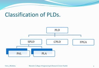
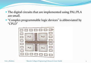
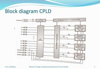
By
Mr. C.R.Shinde
Electrical Engineering Department
Matoshri College of Engineering & Research centre, Nashik
Unit 03: Digital memories and logic families
Digital memories:
SRAM, DRAM, ROM, EPROM
Digital logic families:
PAL,PLA, CPLD, FPGA
Unit 3_Module5 Matoshri College of Engineering & Research Center Nashik 2
Module5 :- CPLD, FPGA
Unit 3_Module5 Matoshri College of Engineering & Research Center Nashik 3
1. Introduction to CPLD & FPGA.
2. Block Diagram of CPLD & FPGA.
3. Advantages & Disadvantage of PLA.
4. Comparison of CPLD & FPGA.
Classification of PLDs.
PLD
SPLD
PAL PLA
CPLD FPGA
Unit 3_Module5 Matoshri College of Engineering & Research Center Nashik 4
Unit 3_Module5 Matoshri College of Engineering & Research Center Nashik 5
 The digital circuits that are implemented using PAL/PLA
are small.
 “Complex programmable logic devices” is abbreviated by
“CPLD”
Block diagram CPLD
Unit 3_Module5 Matoshri College of Engineering & Research Center Nashik 6
Module 4
Unit 3_Module5 Matoshri College of Engineering & Research Center Nashik 7
1. Introduction.
2. Block Diagram of PLA.
3. Basic Structure of PLA.
4. Advantages & Disadvantage of PLA.
5. Comparison of PAL & PLA
Thank you
Mr. C. R. Shinde
Electrical Engineering Department
Matoshri College of Engineering & Research centre, Nashik
If you have any query, ask me anytime on…… … .. . . .
cshinde58@gmail.com
chandrakant.shinde@matoshri.edu.in
9970031353
Unit 3_Module5
Matoshri College of Engineering & Research Center
Nashik 8
Parameter FPGA CPLD
Unit 3_Module5 Matoshri College of Engineering & Research Center Nashik 9

Module 5: CPLD & FPGA

  • 1.
    By Mr. C.R.Shinde Electrical EngineeringDepartment Matoshri College of Engineering & Research centre, Nashik
  • 2.
    Unit 03: Digitalmemories and logic families Digital memories: SRAM, DRAM, ROM, EPROM Digital logic families: PAL,PLA, CPLD, FPGA Unit 3_Module5 Matoshri College of Engineering & Research Center Nashik 2
  • 3.
    Module5 :- CPLD,FPGA Unit 3_Module5 Matoshri College of Engineering & Research Center Nashik 3 1. Introduction to CPLD & FPGA. 2. Block Diagram of CPLD & FPGA. 3. Advantages & Disadvantage of PLA. 4. Comparison of CPLD & FPGA.
  • 4.
    Classification of PLDs. PLD SPLD PALPLA CPLD FPGA Unit 3_Module5 Matoshri College of Engineering & Research Center Nashik 4
  • 5.
    Unit 3_Module5 MatoshriCollege of Engineering & Research Center Nashik 5  The digital circuits that are implemented using PAL/PLA are small.  “Complex programmable logic devices” is abbreviated by “CPLD”
  • 6.
    Block diagram CPLD Unit3_Module5 Matoshri College of Engineering & Research Center Nashik 6
  • 7.
    Module 4 Unit 3_Module5Matoshri College of Engineering & Research Center Nashik 7 1. Introduction. 2. Block Diagram of PLA. 3. Basic Structure of PLA. 4. Advantages & Disadvantage of PLA. 5. Comparison of PAL & PLA
  • 8.
    Thank you Mr. C.R. Shinde Electrical Engineering Department Matoshri College of Engineering & Research centre, Nashik If you have any query, ask me anytime on…… … .. . . . cshinde58@gmail.com chandrakant.shinde@matoshri.edu.in 9970031353 Unit 3_Module5 Matoshri College of Engineering & Research Center Nashik 8
  • 9.
    Parameter FPGA CPLD Unit3_Module5 Matoshri College of Engineering & Research Center Nashik 9