The document describes five experiments performed using an 8085 microprocessor kit to understand various arithmetic operations. Experiment 1 adds two 8-bit numbers and stores the 8-bit sum. Experiment 2 adds two 8-bit numbers and stores the 16-bit sum. Experiment 3 adds two 16-bit numbers and stores the 16-bit sum. Experiment 4 performs decimal addition of two 8-bit numbers and stores the 8-bit sum. Experiment 5 finds the one's complement of an 8-bit number.
This document discusses arithmetic operations and conversions using the 8085 microprocessor. It includes algorithms and programs for 8-bit addition, subtraction, multiplication, and division. It also covers sorting algorithms to find the ascending and descending order of numbers, and algorithms to find the minimum and maximum numbers in a data set. Additionally, it explains programs that demonstrate the rotate instructions RLC, RRC, RAL, and RAR. Finally, it provides examples of conversions between ASCII, hexadecimal, and BCD codes.
This document contains a manual for microprocessor lab programs. It lists 30 programs with descriptions and algorithms for tasks like data transfer, sorting, arithmetic operations, conversions, and interfacing. The manual provides a template for writing assembly language programs (ALPs) to perform these tasks on the 8085 microprocessor, including initializing registers, looping structures, logic checks, and displaying results. It also includes sample result sheets showing address-data fields and I/O for several programs.
This presentation discusses the Serial Communication features in 8051, the support for UART. It also discusses serial vs parallel communication, simplex, duplex and full-duplex modes, MAX232, RS232 standards
The assembly language program for multiplying two 8-bit numbers using an 8085 microprocessor is summarized as follows:
1) The program loads the first 8-bit number into register B and the second 8-bit number into register C.
2) It initializes the accumulator and carry flag to zero.
3) It then adds the value of register B to the accumulator and checks the carry flag.
4) If carry is set, it increments the carry flag and if not it jumps to the next step.
5) It decrements the value of register C and repeats the process until register C becomes zero.
6) The final result is stored in the accumulator including any carry value
This document provides an overview of assembly language programming for the 8085 microprocessor. It discusses the 8085 programming model including registers, flags, and addressing modes. The document also covers the instruction set categories such as data transfer, arithmetic, logical and branching instructions. Examples are given to demonstrate how to write an assembly language program for the 8085 including analyzing a problem, developing an algorithm, flowchart, and coding the solution. Input/output and memory addressing modes are also explained.
The document discusses stacks, subroutines, and the 8085 microprocessor. It provides the following key points:
1. The stack is an area of memory used for temporary storage of information in LIFO (last in first out) order, growing backwards into memory with the stack pointer register defining the bottom.
2. Subroutines allow groups of instructions to be called from different locations to avoid repetition. The 8085 uses CALL to redirect execution to a subroutine and RTE to return to the calling routine.
3. Data can be passed to subroutines through registers or memory locations. Proper subroutines only enter at the start and exit at the end, with a single entry point
Assembler directives and basic steps ALP of 8086Urvashi Singh
The document discusses various assembler directives used in assembly language programming. It describes directives like DB, DW, DD, DQ, DT for data declaration; ASSUME to define logical segments; END, ENDP, ENDS to mark ends; EQU to define constants; PROC and ENDP to define procedures; ORG to set the location counter; SEGMENT to define logical segments; GROUP, INCLUDE, EVEN, and ALIGN for segment organization; EXTRN and PUBLIC for external references; and TYPE and PTR for defining variable types. The directives provide necessary information to the assembler to understand assembly language programs and generate machine code.
Stack in microprocessor 8085(presantation)Safin Biswas
The stack is a group of memory locations used for temporary storage during program execution. Information is stored and retrieved from the stack using the PUSH and POP instructions in a LIFO manner. Subroutines allow a group of instructions to be called repeatedly from the main program. The CALL instruction stores the return address on the stack and transfers execution to the subroutine. The RET instruction retrieves the return address from the stack and transfers execution back to the main program.
The document describes a lab experiment on addition of two 8-bit numbers using an 8085 microprocessor. It includes:
1) An algorithm that initializes the carry to zero, loads the two 8-bit numbers into registers, adds the numbers and checks for carry, increments the carry if needed, and stores the result.
2) The assembly language program with labels, mnemonics, hex codes and comments to implement the algorithm.
3) Inputs, outputs and results with and without carry from adding sample 8-bit numbers.
The document discusses various addressing modes and instructions of the 8051 microcontroller. It describes the five addressing modes - immediate, register, direct, register indirect and indexed. It explains each addressing mode in detail. It also explains the various instruction groups - data transfer, arithmetic, logical, boolean and branching instructions. It provides examples of instructions like MOV, ADD, ANL, JMP etc. and how they are used to manipulate data in the 8051.
The document is a lab manual for a Microprocessor and Microcontroller lab. It contains:
1. An introduction and syllabus covering digital and linear circuits, 8-bit microprocessors and microcontrollers, and various experiments.
2. Details of experiments with an 8-bit microprocessor (8085) including arithmetic operations, sorting/searching arrays, code conversions, and interfacing analog devices.
3. Details of experiments with an 8-bit microcontroller (8051) including programming basics and interfacing devices like stepper motors.
4. Objectives, apparatus, algorithms, programs, procedures, inputs/outputs for each experiment.
The 8086 instruction set includes 8 categories of instructions: data transfer, arithmetic, branch, loop, machine control, flag manipulation, shift/rotate, and string instructions. Some key instructions include MOV for data transfer, PUSH/POP for stack operations, ADD/SUB for arithmetic, JMP for branching, LOOP for looping, and SHIFT/ROTATE for bitwise operations.
The 8051 microcontroller has 128 bytes of internal RAM and 4Kbytes of internal ROM memory. It uses the same addresses for code and data but accesses the correct memory based on whether an operation is for code or data. The 128 bytes of internal RAM are organized into 4 banks of 32 bytes each. External memory can be added if more memory is needed for program code or variable data storage. The document also provides information on interfacing external program and data memory with the 8051 microcontroller.
The document discusses the 8051 microcontroller. It describes the basic components of the 8051 including 4K bytes of internal ROM, 128 bytes of internal RAM, four 8-bit I/O ports, two 16-bit timers/counters, and one serial interface. It provides a block diagram of the 8051 and discusses important pins such as the I/O ports, PSEN, ALE, EA, RXD, TXD, and XTAL1 and XTAL2. It also gives examples of how the 8051 is used in embedded systems and describes methods for connecting an external clock source to the 8051.
Microprocessor and Microcontroller Lab ManualSanthosh Kumar
The document describes assembly language programs to perform simple arithmetic operations, sorting of arrays, and finding the largest/smallest element in an array using 8085 microprocessor. It includes algorithms, flowcharts and programs for addition, subtraction, multiplication, division, ascending/descending sorting of an array, and finding the largest element in an array. The programs demonstrate performing arithmetic operations on data stored in memory locations and comparing/moving data between registers and memory.
The document contains programs to perform various operations on 8-bit numbers like addition, subtraction, multiplication, division using 8085 microprocessor. It also contains programs to find the largest/smallest number in an array, and to arrange an array of numbers in ascending order. The programs demonstrate various instructions of 8085 like load, move, add, subtract, compare, jump etc to perform the given tasks.
Introduction to 8085 & it's description(includes basic lab experiments)Basil John
The document provides information about the 8085 microprocessor. It describes the 8085 as an 8-bit microprocessor capable of addressing 64KB of memory. It then details the various functional blocks of the 8085 including general purpose registers, accumulator, program counter, stack pointer, ALU, flags register, timing and control unit, and instruction register and decoder. Finally, it provides examples of assembly language programs for 8-bit addition, subtraction, and 16-bit addition and subtraction on the 8085 microprocessor.
Register Organisation of 8086 MicroprocessorNikhil Kumar
The document discusses the registers used in the 8086 microprocessor. It describes the different types of registers: general purpose registers like AX, BX, CX, and DX which can be used for data and addressing; segment registers like CS, SS, DS and ES that store segment offsets; pointer and index registers like IP, BP, SP, SI and DI that contain memory addresses; and flag registers that indicate results of arithmetic logic unit operations and control the CPU. The document provides details on the individual registers and their purposes in the 8086 architecture.
The 8155 and 8156 microprocessor interface chips differ in that the 8155 has an active low Chip Enable (CE) signal, while the 8156 has an active high CE signal. The 8155 is a multifunction chip that contains RAM, I/O ports, and a timer. It has two 8-bit I/O ports, one 6-bit I/O port, a 14-bit counter/timer, 2Kb of RAM, and can be interfaced with the 8085 microprocessor. The document then provides details on the pinout, memory mapping, control register, port configurations, timer operation modes, and status register of the 8155 chip.
The document discusses the architecture of the Intel 8085 microprocessor. It describes the 8085 as an 8-bit microprocessor introduced in 1976 that uses a single +5 volt power supply. The internal architecture includes a control unit, arithmetic logic unit (ALU), registers including the accumulator, program counter, stack pointer, instruction register/decoder, and timing and control unit. The document also briefly discusses interrupts, serial I/O, and some applications of microprocessors like mobile phones, watches, and appliances.
The 8086 microprocessor is a 16-bit CPU launched by Intel in 1978. It has a 16-bit data bus and 20-bit address bus, allowing it to access up to 1MB of memory. The 8086 architecture partitions the CPU logic into two functional units - the Bus Interface Unit which handles external transactions, and the Execution Unit which performs decoding and execution. This separation improves processing speed by allowing parallel instruction fetching and execution via pipelining. The 8086 uses memory segmentation to access more memory than its 16-bit registers allow, dividing the 1MB address space into 64KB segments addressed using segment and offset registers.
The document summarizes memory organization and addressing in the 8086 microprocessor. It discusses that the 8086 has a 20-bit address bus that can access 1MB of memory. Memory is organized into two 512KB banks to allow 16-bit words to be accessed with a single machine cycle. Data can be accessed from memory in four ways - as 8-bit quantities from the even or odd bank, or as 16-bit words from even or odd addresses, which may require one or two cycles respectively. The document provides details on the signals used to control memory bank selection and addressing.
Interfacing memory with 8086 microprocessorVikas Gupta
This document discusses interfacing memory with the 8086 microprocessor. It begins by defining different types of memory like RAM, ROM, EPROM, and EEPROM. It then discusses memory fundamentals like capacity, organization, and standard memory ICs. The document explains two methods of address decoding - absolute and partial decoding. It provides examples of interfacing 32KB RAM, 32K words of memory, and a combination of ROM, EPROM, and RAM with the 8086 using address decoding techniques. Diagrams and tables are included to illustrate the memory mapping and generation of chip select logic.
This document provides an overview of analog to digital converters (ADCs) and describes how to interface the ADC0804 and ADC0808/0809 chips with an 8051 microcontroller. It discusses the basic functions and pinouts of the ADC0804 chip, how to convert analog voltages to digital values using its reference pin, and the steps to read output data. It also covers the channel selection, reference voltage, and programming steps for the 8-channel ADC0808/0809 chip. Timing diagrams are included to illustrate the read and write processes.
This document provides an overview of the instruction set of the 8085 microprocessor. It begins by defining what an instruction is and the classification of the 8085 instruction set. It then proceeds to describe various data transfer, arithmetic, logical, branching, and control instructions in detail through opcode, operands, examples, and before/after execution illustrations. The document aims to provide a comprehensive reference for the complete set of 246 instructions supported by the 8085 microprocessor.
This document discusses memory interfacing with the 8085 microprocessor. It begins by describing the different types of computer memory, including primary/volatile memory (RAM and ROM) and secondary/non-volatile memory (magnetic tapes, disks, optical disks). It then discusses how the 8085 microprocessor interfaces with memory chips through an interface circuit. The interface circuit matches the memory chip signals to the microprocessor address and control signals. Memory interfacing involves selecting the appropriate memory chip, identifying the correct register using address lines, and enabling read/write buffers using control signals.
The document contains notes on microprocessors and interfacing prepared by Akshansh Chaudhary for a course at BITS Pilani in 2013. It includes content on microprocessors, microcontroller basics, assembly language programming, and interfacing concepts. The notes were prepared based on a course by Susanna S. Henry and include copyright information and disclaimers regarding use of the content.
The document discusses assembly language programs for arithmetic operations and data conversions using an 8085 microprocessor. It includes algorithms and programs for 8-bit addition, subtraction, multiplication, and division. It also covers sorting data in ascending and descending order, finding minimum and maximum values, and performing rotate instructions. Additional programs are provided for converting between ASCII, hexadecimal, and BCD codes.
This document discusses the assembly language programming of the 8085 microprocessor. It covers the basic topics of the 8085 instruction set including data transfer, arithmetic, logical and branching instructions. It also describes the addressing modes, programming model and instruction formats of the 8085 assembly language. Examples of assembly language instructions are provided to illustrate how to perform common operations like loading registers, arithmetic, and conditional jumps.
The document provides an overview of assembly language programming for the 8085 microprocessor. It discusses the 8085 programming model including registers, flags, and addressing modes. It also describes the instruction set categories and provides examples of common instruction types like data transfer, arithmetic, logical, and branching instructions. Sample assembly language programs are shown to add two numbers and handle results larger than 8 bits.
The document provides an overview of the 8085 microprocessor programming model. It describes the hardware model including the ALU, accumulator, registers, buses, and flags. It also discusses the programming model, instruction set classification including data transfer, arithmetic, logical, and branching operations. Finally, it covers instruction word sizes, opcode format, and data formats like ASCII, BCD, signed and unsigned integers.
Programming with 8085-Microprocessor and interfacingAmitabh Shukla
Here are the key steps to separate the digits of a hexadecimal number and store them in two locations:
1. Load the packed BCD number into the accumulator register using LDA instruction
2. Mask the lower nibble using ANI instruction with F0H to isolate the lower digit
3. Rotate the accumulator right through carry three times using RRC instruction to shift the higher digit into the lower position
4. Store the lower and higher digits into two separate memory locations
This separates the digits of the hexadecimal number by isolating and adjusting the position of each digit, allowing them to be stored independently.
The document discusses the 8085 microprocessor instruction set and addressing modes. It contains the following key points:
1) The 8085 has 74 instructions that are grouped into 5 categories - data transfer, arithmetic, logical, branch, and machine control operations. Most instructions have multiple formats.
2) Instructions are 1, 2, or 3 bytes in size depending on the operands. The opcode specifies the operation and registers while the operands provide data or addresses.
3) There are 5 addressing modes including register, immediate, direct, indirect, and implied that specify how operands are addressed in memory.
4) A sample program is provided to add two numbers and display the result using MVI, ADD, and
The document provides information about the 8085 microprocessor. It describes the 8085 as an 8-bit processor with 40 pins that can access 64KB of memory and 256 I/O ports. It has 5 hardware interrupts, 8 general purpose registers including the program counter and stack pointer, and provides 74 instructions across 5 addressing modes.
8085 Paper Presentation slides,ppt,microprocessor 8085 ,guide, instruction setSaumitra Rukmangad
The document provides information about the 8085 microprocessor. It describes the 8085 as an 8-bit processor with 40 pins that can access 64KB of memory and 256 I/O ports. It has 5 hardware interrupts, 8 general purpose registers including the program counter and stack pointer, and provides 74 instructions across 5 addressing modes.
This document provides an overview of programming with the 8085 microprocessor using assembly language. It discusses the 8085 programming model including registers, flags, and addressing modes. It also covers the instruction set categories such as data transfer, arithmetic, logical, and branching operations. Examples are given of writing assembly language programs, including adding two numbers, handling results larger than 8 bits, and separating digits of a hexadecimal number. The document is intended to teach assembly language programming for the 8085 microprocessor.
1. The document discusses basic programming of the 8085 microprocessor. It covers the different types of programming languages including machine language, assembly language, and high-level languages.
2. The 8085 instruction set is classified into different groups like data transfer, arithmetic, logical, branch, and machine control instructions. Common instructions like MOV, ADD, SUB, and CALL are described.
3. The document provides examples of 8085 programs and instructions to load data, perform arithmetic operations, manage the stack, handle I/O, and control program flow. It also discusses assembler format and use of registers like the accumulator, flag register, and stack pointer.
The document provides information about the 8085 microprocessor. Some key points:
- The 8085 is an 8-bit processor with 40 pins that uses a multiplexed address/data bus. It operates at clock speeds from 500kHz to 3MHz.
- It has 16 address lines allowing access to 64KB of memory. It provides 5 hardware interrupts and contains registers like the accumulator, flag register, and 6 general purpose registers.
- Important pins include the AD bus, address lines A8-A15, control signals like ALE, RD, WR and status signals like READY. It also has pins for serial I/O and interrupts.
- The architecture includes the arithmetic logic unit,
The document describes a lab manual for experiments with an 8085 microprocessor. It includes:
1) 13 assembly language programs to perform operations like data transfer, addition, comparison etc. using the 8085 microprocessor kit.
2) Details of the 8085 microprocessor architecture including registers, flags, pin descriptions.
3) Information about the memory map, I/O ports, and other integrated circuits used in the microprocessor kit like 8253, 8255, 8279.
4) Procedures for entering and executing programs on the microprocessor kit and expected input/output for programs.
The document provides comprehensive information needed to learn and perform various experiments on an 8085 microprocessor
Question bank on Microcontroller 8051/AT89C51. Total 98 questions. Covering questions on introduction, programming, timers of 8051, serial communication of 8051, interrupts of 8051, memory interfacing, and applications.
Microprocessor and Microcontroller Lab Manual!PRABHAHARAN429
The document describes experiments to be performed on an 8-bit microprocessor and microcontroller. It includes aims, block diagrams, flowcharts and assembly language programs for arithmetic operations, sorting an array, and interfacing experiments. Experiments cover topics like addition, subtraction, multiplication, division, ascending/descending order, maximum/minimum values, and interfacing components like ADCs, DACs, stepper motors. Similar experiments are outlined for an 8-bit microcontroller.
1. This document contains a question bank for the subject Microprocessor and Assembly Language Programming for the 4th semester BME course. It includes questions related to microprocessor architecture, memory, interrupts, instruction sets, programming techniques and medical applications of microprocessors.
2. The questions cover topics such as 8085 and 8086 microprocessor architecture, memory organization, addressing modes, instruction formats, timing diagrams, assembly language programming, RISC and CISC processors, temperature monitoring and ECG systems using microprocessors.
3. Sample questions include explaining the pin diagram of 8085, comparing Von Neumann and Harvard architectures, writing programs to transfer and manipulate data, explaining interrupts and addressing modes, drawing block diagrams of processors like
The document describes the 8085 microprocessor, including its pin diagram, functional units, architecture, and example assembly language programs. Specifically, it provides details on the 8085's power supply and frequency pins, data and address buses, control signals, interrupt signals, and serial and DMA signals. It outlines the 8085's functional units like the accumulator, arithmetic logic unit, registers, and timing and control unit. Example programs are provided to exchange 16-bit numbers, add and subtract 8-bit and 16-bit numbers, and add two N-byte numbers.
This document describes the instruction set of the 8085 microprocessor. It includes descriptions of various instruction groups such as data transfer instructions, arithmetic instructions, logical instructions, branch instructions, stack instructions, I/O instructions, and machine control instructions. Diagrams are provided explaining the program status word register flags and addressing modes used by the 8085 instruction set. Examples of specific instructions like MVI, LXI, and PUSH are also referenced.
Similar to microprocessor Laboratory experiments manual (20)
The document discusses the benefits of exercise for mental health. Regular physical activity can help reduce anxiety and depression and improve mood and cognitive functioning. Exercise causes chemical changes in the brain that may help protect against mental illness and improve symptoms.
The document discusses the benefits of exercise for mental health. Regular physical activity can help reduce anxiety and depression and improve mood and cognitive functioning. Exercise causes chemical changes in the brain that may help boost feelings of calmness, happiness and focus.
The document discusses the benefits of exercise for mental health. Regular physical activity can help reduce anxiety and depression and improve mood and cognitive function. Exercise causes chemical changes in the brain that may help protect against developing mental illness and improve symptoms for those who already suffer from conditions like anxiety and depression.
The document discusses the results of a study on the effects of a new drug on memory and cognitive function in older adults. The double-blind study involved 100 participants aged 65-80 who were given either the drug or a placebo daily for 6 months. Researchers found that those who received the drug performed significantly better on memory and problem-solving tests at the end of the study compared to those who received the placebo.
The document discusses the benefits of exercise for mental health. Regular physical activity can help reduce anxiety and depression and improve mood and cognitive functioning. Exercise stimulates the production of endorphins in the brain which elevate mood and reduce stress levels.
The document discusses the benefits of exercise for mental health. Regular physical activity can help reduce anxiety and depression and improve mood and cognitive functioning. Exercise boosts blood flow and levels of serotonin and endorphins which elevate mood and may help prevent mental illness.
Top 1000 Java Interview Questions Includes Spring, Hibernate, Microservices, ...Ankit Kumar
This document provides an overview and table of contents for a book titled "Top 1000 Java Interview Questions & Answers" by Knowledge Powerhouse. It includes the copyright information, a dedication, and lists chapter titles covering topics like Java basics, OOP principles, inheritance, static methods, method overloading and overriding, polymorphism, abstraction, final keywords, packages, internationalization, serialization, reflection, garbage collection, inner classes, strings, exception handling, multi-threading, and collections. The document gives a high-level outline of the technical concepts and questions that will be covered in the book.
The document discusses network operating systems and provides an overview of UNIX/Linux operating systems. It covers the history and development of UNIX, differences between UNIX variants like FreeBSD and Linux, and components of operating systems like processes, memory management, and file systems. It also gives examples of process information using the ps command.
Ethernet uses different cabling standards depending on the technology. 10BASE5 uses thick coaxial cable allowing distances of 500 meters, while 10BASE2 uses thinner coaxial cable allowing 185 meters. 10BASE-T networks used hubs, creating a shared media where only one station could transmit at a time (half-duplex). Newer technologies like 100BASE-TX use switches to isolate each port and allow full-duplex communication. Ethernet standards also use different encoding schemes like Manchester encoding for 10BASE-T and 4B/5B encoding for Fast Ethernet.
This document compares and contrasts IPv4 and IPv6. It notes that IPv4 uses 32-bit addresses which limits the number of available addresses, while IPv6 uses 128-bit addresses providing vastly more unique addresses to meet future network growth. It describes several new features of IPv6 including separate options fields to speed routing, additional security options like encryption, and quality of service controls. IPv6 was designed to support greater Internet usage, high-speed transmission of audio/video, and next generation networking needs.
This document discusses remote procedure calls and data conversion when communicating between computers with different architectures. It describes Abstract Syntax Notation and External Data Representation as two available methods for data conversion. Remote procedure calls allow a client to call a procedure on a remote server as if it were a local procedure call. The client stub marshals parameters and sends them to the server stub, which unmarshals the parameters and calls the server procedure before returning any results.
The document discusses various ways to classify signals. Signals can be classified based on parameters such as the independent variable (e.g. continuous time vs. discrete time signals), dependent variable (e.g. analog vs. digital signals), number of independent variables (e.g. one-dimensional, two-dimensional, multi-dimensional signals), periodicity (e.g. periodic vs. aperiodic signals), determinism (e.g. deterministic vs. random signals), causality (e.g. causal, anti-causal, non-causal signals), and energy content (e.g. energy signals, power signals). Continuous time signals have values defined over a continuum of time, while discrete time signals
The document discusses the benefits of exercise for mental health. Regular physical activity can help reduce anxiety and depression and improve mood and cognitive functioning. Exercise causes chemical changes in the brain that may help protect against mental illness and improve symptoms.
The document provides a lab manual for computer graphics experiments in C language. It includes experiments on digital differential analyzer algorithm, Bresenham's line drawing algorithm, midpoint circle generation algorithm, ellipse generation algorithm, text and shape creation, 2D and 3D transformations, curve generation, and basic animations. It outlines the hardware and software requirements to run the experiments and provides background, algorithms, sample programs and outputs for each experiment.
Training completion certificate of b.s.n.lAnkit Kumar
This certificate certifies that Ankush (14152011), a final year ECE student, successfully completed summer training as required for their B.Tech degree from the university. The training took place during the 2009-2010 academic year and this report documents the authentic work completed by the student during that period.
Training completion certificate of b.s.n.l (2)Ankit Kumar
BSNL is an Indian state-owned telecommunications company that was incorporated in 2000 and took over telecom services from government departments, making it the largest provider of fixed telephony and broadband in India with over 60% market share. However, BSNL has faced heavy losses in recent years due to intense competition. It is India's oldest communication service provider and had over 93 million customers as of 2015, present throughout India except for Mumbai and New Delhi.
This document provides a table of contents for chapters in a book or document on telecommunications networks. It includes chapters on BSNL (Bharat Sanchar Nigam Limited), basic telecom networks, leased lines, intranets, corporate networks, Wi-Fi, WiMAX, GSM, and optical fiber transmission. The table of contents lists topics like call setup, electronic exchanges, carrier rooms, main distribution frames, power plants, managed leased line networks, intranet applications, and features of corporate networks. It also includes figures and tables related to the topics.
This is a summer training report submitted by a student to Mrs. at Guru Jambeshwar University of Science & Technology in Hisar, Haryana, India. The report provides information from a summer training conducted by the student at the university.
DEEP LEARNING FOR SMART GRID INTRUSION DETECTION: A HYBRID CNN-LSTM-BASED MODELgerogepatton
As digital technology becomes more deeply embedded in power systems, protecting the communication
networks of Smart Grids (SG) has emerged as a critical concern. Distributed Network Protocol 3 (DNP3)
represents a multi-tiered application layer protocol extensively utilized in Supervisory Control and Data
Acquisition (SCADA)-based smart grids to facilitate real-time data gathering and control functionalities.
Robust Intrusion Detection Systems (IDS) are necessary for early threat detection and mitigation because
of the interconnection of these networks, which makes them vulnerable to a variety of cyberattacks. To
solve this issue, this paper develops a hybrid Deep Learning (DL) model specifically designed for intrusion
detection in smart grids. The proposed approach is a combination of the Convolutional Neural Network
(CNN) and the Long-Short-Term Memory algorithms (LSTM). We employed a recent intrusion detection
dataset (DNP3), which focuses on unauthorized commands and Denial of Service (DoS) cyberattacks, to
train and test our model. The results of our experiments show that our CNN-LSTM method is much better
at finding smart grid intrusions than other deep learning algorithms used for classification. In addition,
our proposed approach improves accuracy, precision, recall, and F1 score, achieving a high detection
accuracy rate of 99.50%.
Electric vehicle and photovoltaic advanced roles in enhancing the financial p...IJECEIAES
Climate change's impact on the planet forced the United Nations and governments to promote green energies and electric transportation. The deployments of photovoltaic (PV) and electric vehicle (EV) systems gained stronger momentum due to their numerous advantages over fossil fuel types. The advantages go beyond sustainability to reach financial support and stability. The work in this paper introduces the hybrid system between PV and EV to support industrial and commercial plants. This paper covers the theoretical framework of the proposed hybrid system including the required equation to complete the cost analysis when PV and EV are present. In addition, the proposed design diagram which sets the priorities and requirements of the system is presented. The proposed approach allows setup to advance their power stability, especially during power outages. The presented information supports researchers and plant owners to complete the necessary analysis while promoting the deployment of clean energy. The result of a case study that represents a dairy milk farmer supports the theoretical works and highlights its advanced benefits to existing plants. The short return on investment of the proposed approach supports the paper's novelty approach for the sustainable electrical system. In addition, the proposed system allows for an isolated power setup without the need for a transmission line which enhances the safety of the electrical network
Harnessing WebAssembly for Real-time Stateless Streaming PipelinesChristina Lin
Traditionally, dealing with real-time data pipelines has involved significant overhead, even for straightforward tasks like data transformation or masking. However, in this talk, we’ll venture into the dynamic realm of WebAssembly (WASM) and discover how it can revolutionize the creation of stateless streaming pipelines within a Kafka (Redpanda) broker. These pipelines are adept at managing low-latency, high-data-volume scenarios.
Embedded machine learning-based road conditions and driving behavior monitoringIJECEIAES
Car accident rates have increased in recent years, resulting in losses in human lives, properties, and other financial costs. An embedded machine learning-based system is developed to address this critical issue. The system can monitor road conditions, detect driving patterns, and identify aggressive driving behaviors. The system is based on neural networks trained on a comprehensive dataset of driving events, driving styles, and road conditions. The system effectively detects potential risks and helps mitigate the frequency and impact of accidents. The primary goal is to ensure the safety of drivers and vehicles. Collecting data involved gathering information on three key road events: normal street and normal drive, speed bumps, circular yellow speed bumps, and three aggressive driving actions: sudden start, sudden stop, and sudden entry. The gathered data is processed and analyzed using a machine learning system designed for limited power and memory devices. The developed system resulted in 91.9% accuracy, 93.6% precision, and 92% recall. The achieved inference time on an Arduino Nano 33 BLE Sense with a 32-bit CPU running at 64 MHz is 34 ms and requires 2.6 kB peak RAM and 139.9 kB program flash memory, making it suitable for resource-constrained embedded systems.
Literature Review Basics and Understanding Reference Management.pptxDr Ramhari Poudyal
Three-day training on academic research focuses on analytical tools at United Technical College, supported by the University Grant Commission, Nepal. 24-26 May 2024
Understanding Inductive Bias in Machine LearningSUTEJAS
This presentation explores the concept of inductive bias in machine learning. It explains how algorithms come with built-in assumptions and preferences that guide the learning process. You'll learn about the different types of inductive bias and how they can impact the performance and generalizability of machine learning models.
The presentation also covers the positive and negative aspects of inductive bias, along with strategies for mitigating potential drawbacks. We'll explore examples of how bias manifests in algorithms like neural networks and decision trees.
By understanding inductive bias, you can gain valuable insights into how machine learning models work and make informed decisions when building and deploying them.
Comparative analysis between traditional aquaponics and reconstructed aquapon...bijceesjournal
The aquaponic system of planting is a method that does not require soil usage. It is a method that only needs water, fish, lava rocks (a substitute for soil), and plants. Aquaponic systems are sustainable and environmentally friendly. Its use not only helps to plant in small spaces but also helps reduce artificial chemical use and minimizes excess water use, as aquaponics consumes 90% less water than soil-based gardening. The study applied a descriptive and experimental design to assess and compare conventional and reconstructed aquaponic methods for reproducing tomatoes. The researchers created an observation checklist to determine the significant factors of the study. The study aims to determine the significant difference between traditional aquaponics and reconstructed aquaponics systems propagating tomatoes in terms of height, weight, girth, and number of fruits. The reconstructed aquaponics system’s higher growth yield results in a much more nourished crop than the traditional aquaponics system. It is superior in its number of fruits, height, weight, and girth measurement. Moreover, the reconstructed aquaponics system is proven to eliminate all the hindrances present in the traditional aquaponics system, which are overcrowding of fish, algae growth, pest problems, contaminated water, and dead fish.
ACEP Magazine edition 4th launched on 05.06.2024Rahul
This document provides information about the third edition of the magazine "Sthapatya" published by the Association of Civil Engineers (Practicing) Aurangabad. It includes messages from current and past presidents of ACEP, memories and photos from past ACEP events, information on life time achievement awards given by ACEP, and a technical article on concrete maintenance, repairs and strengthening. The document highlights activities of ACEP and provides a technical educational article for members.
International Conference on NLP, Artificial Intelligence, Machine Learning an...gerogepatton
International Conference on NLP, Artificial Intelligence, Machine Learning and Applications (NLAIM 2024) offers a premier global platform for exchanging insights and findings in the theory, methodology, and applications of NLP, Artificial Intelligence, Machine Learning, and their applications. The conference seeks substantial contributions across all key domains of NLP, Artificial Intelligence, Machine Learning, and their practical applications, aiming to foster both theoretical advancements and real-world implementations. With a focus on facilitating collaboration between researchers and practitioners from academia and industry, the conference serves as a nexus for sharing the latest developments in the field.
Introduction- e - waste – definition - sources of e-waste– hazardous substances in e-waste - effects of e-waste on environment and human health- need for e-waste management– e-waste handling rules - waste minimization techniques for managing e-waste – recycling of e-waste - disposal treatment methods of e- waste – mechanism of extraction of precious metal from leaching solution-global Scenario of E-waste – E-waste in India- case studies.
Presentation of IEEE Slovenia CIS (Computational Intelligence Society) Chapte...University of Maribor
Slides from talk presenting:
Aleš Zamuda: Presentation of IEEE Slovenia CIS (Computational Intelligence Society) Chapter and Networking.
Presentation at IcETRAN 2024 session:
"Inter-Society Networking Panel GRSS/MTT-S/CIS
Panel Session: Promoting Connection and Cooperation"
IEEE Slovenia GRSS
IEEE Serbia and Montenegro MTT-S
IEEE Slovenia CIS
11TH INTERNATIONAL CONFERENCE ON ELECTRICAL, ELECTRONIC AND COMPUTING ENGINEERING
3-6 June 2024, Niš, Serbia
Redefining brain tumor segmentation: a cutting-edge convolutional neural netw...IJECEIAES
Medical image analysis has witnessed significant advancements with deep learning techniques. In the domain of brain tumor segmentation, the ability to
precisely delineate tumor boundaries from magnetic resonance imaging (MRI)
scans holds profound implications for diagnosis. This study presents an ensemble convolutional neural network (CNN) with transfer learning, integrating
the state-of-the-art Deeplabv3+ architecture with the ResNet18 backbone. The
model is rigorously trained and evaluated, exhibiting remarkable performance
metrics, including an impressive global accuracy of 99.286%, a high-class accuracy of 82.191%, a mean intersection over union (IoU) of 79.900%, a weighted
IoU of 98.620%, and a Boundary F1 (BF) score of 83.303%. Notably, a detailed comparative analysis with existing methods showcases the superiority of
our proposed model. These findings underscore the model’s competence in precise brain tumor localization, underscoring its potential to revolutionize medical
image analysis and enhance healthcare outcomes. This research paves the way
for future exploration and optimization of advanced CNN models in medical
imaging, emphasizing addressing false positives and resource efficiency.
Redefining brain tumor segmentation: a cutting-edge convolutional neural netw...
microprocessor Laboratory experiments manual
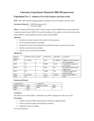
1. Laboratory Experiments Manual for 8085 Microprocessor
Experiment No. 1 - Addition of Two 8-bit Numbers and Sum is 8-bit
AIM: Write 8085 assembly language program for addition of two 8-bit numbers and sum is 8 bit.
Instruments Required: 1. 8085 Microprocessor Kit
2. +5V Power supply
Theory : Consider the first number 26H is stored in memory location 8000H and the second number 62H
is stored in memory location 8001H. The result after addition of two numbers is to be stored in the memory
location 8002 H. Assume program starts from memory location 8500H.
Algorithm
1. Initialise the memory location of first number in HL register pair.
2. Move first number/data into accumulator
3. Increment the content of HL register pair to initialise the memory location of second data
4. Add the second data with accumulator
5. Store the result in memory location 8003H
PROGRAM
Memory
address
Machine Codes Labels Mnemonics Operands Comments
8500 21, 00, 80 LXI H, 8000 H Address of first number in
H-L register pair.
8503 7E MOV A,M Transfer first number in
accumulator.
8504 23 INX H Increment content of H-L
register pair
8505 66 ADD M Add first number and
second number
8506 32, 03, 80 STA 8003H Store sum in 8003 H
8509 76 HLT Halt
Experimental Results
Input DATA RESULT
Memory location Data Memory location Data
8000 26H
8001 62H
8003 88H
Conclusion:
The addition of two 8-bit numbers is performed using 8085 microprocessor where sum is 8-bit.
Precautions:
1. Properly connect the 8085 microprocessor kit with power supply terminals.
2. Switch on the power supply after checking connections
3. Handle the Trainer kit carefully.
Viva-Voice Questions:
2. 1. What is the function of LXI H, 8000 H instruction?
2. How you can store a data in a memory location?
3. How you can read a data from a memory location?
4. What are flags available in 8085 ?
5. What is the function of RESET key of a 8085 microprocessor kit
Experiment No. 2 - Addition of two 8 bit numbers and sum is 16-bit
AIM: Write 8085 assembly language program for addition of two 8-bit numbers and sum is 16 bit.
Instruments Required: 1. 8085 Microprocessor Kit
2. +5V Power supply
Theory : The first number F2H is stored in memory location 8501H and the second number 2FH is stored
in memory location 8502H. The result after addition will be stored in the memory location 8503 H and
8504H. Consider program is written from memory location 8000H.
Algorithm:
Initialise the memory location of 1st
data in HL register pair.
Store first data in the memory location
Increment the content of HL register pair for entering next data in the next memory location
Store second data in the memory location
Move second number in accumulator
Decrease the content of HL register pair
Add the content of memory (first data) with accumulator
Store the results in memory location 8503H and 8504H.
PROGRAM
Memory
address
Machine Codes Labels Mnemonics Operands Comments
8000 21, 01, 85 LXI H, 8501 H Address of 1st
number in
H-L register pair.
8003 36, F2 MVI M, F2H Store 1st
number in
memory location
represented by H-L
register pair.
8005 23 INX H Increment content of H-L
register pair
8006 36, 2F MVI M, 2FH Store 2nd
number in
memory location
represented by H-L
register pair
8008 7E MOV A, M 2nd
number in accumulator
8009 0E, 00 MVI C,00H Initialise C register with
00H to store MSBs of sum
800B 2B DCX H Address of 1st
number
3. 2501 in H-L pair
800C 66 ADD M Addition of 1st
number
and 2nd
number
800D D2, 11, 85 JNC LEVEL_1 If carry does not
generated , jump to
LEVEL_1 ?
8010 0C INR C When carry is generated,
increment C register.
8011 32, 03, 85 LEVEL_1 STA 8503H Store LSBs of sum in
memory location 8503H
8014 79 MOV A,C Move MSBs of sum in
accumulator
8015 32, 04, 85 STA 2504 H Store MSBs of sum in
memory location 8503H.
8018 76 HLT Halt
Experimental Results
Input DATA RESULT
Memory location Data Memory location Data
8501 F2H 8503 82H LSBs of sum
8502 2FH 8504 01H MSBs of sum
Conclusion:
The addition of two 8-bit numbers is performed using 8085 microprocessor where sum is 16-bit.
Precautions:
Properly connect the 8085 microprocessor kit with power supply terminals.
Switch on the power supply after checking connections
Handle the Trainer kit carefully.
Viva-Voice Questions:
1. What is the function of JNC instruction?
2. What is the difference between conditional and unconditional jump instruction?
3. What is the function of STA 2500$ instruction?
4. What is multi byte?
Experiment No. 3 - Addition of Two 16-Bit Numbers and Sum is 16-bit
AIM: Write 8085 assembly language program for addition of two16-bit numbers and sum is 16 bit.
Instruments Required: 1. 8085 Microprocessor Kit
2. +5V Power supply
Theory : The first 16-bit number is stored in 8501 and 8502 memory locations. The second 16-bit number
is stored in 8503 and 8504 memory locations. After addition result will be stored from 8505 and 8506
memory locations. Assume program starts from memory location 8000H
4. Algorithm:
1. Store first 16-bit number in H-L pair.
2. Exchange the contents of D-E pair and H-L pair to store first number in D-E registers pair.
3. Store second 16-bit number in HL register pair.
4. Addition of 1st
and 2nd
number
5. Store result in 8505H and 8506H locations.
PROGRAM
Memory
address
Machine Codes Labels Mnemonics Operands Comments
8000 2A, 01, 85 LHLD 8501 H Load the content of 8501H
location in L register and H
register is loaded with the
content of 8502H location.
8000 EB XCHG` The contents of HL register
pair are exchanged with
D-E register pair. So that
first data is stored in DE
register pair.
8000 2A, 03, 85 LHLD 8503 H Load second 16-bit number
(data-2) in H-L pair.
8000 19 DAD D The contents of D-E pair
are added with the contents
of H-L pair and result is
stored in H-L pair.
8000 22, 05, 85 SHLD 8505 H Store LSBs of sum in 8505
and MSBs of sum 8506 H.
8000 76 HLT Halt
Experimental Results
Input DATA RESULT
Memory location Data Memory
location
Data
8501 05H LSBs of data-1 8505 07H LSBs of sum
8502 01H MSBs of data-1 8506 04H MSBs of sum
8503 02H LSBs of data-2
8504 03H MSBs of data-2
Conclusion:
The addition of two 16-bit numbers is performed using 8085 microprocessor where sum is 16-bit.
Precautions:
1. Properly connect the 8085 microprocessor kit with power supply terminals.
2. Switch on the power supply after checking connections
3. Handle the Trainer kit carefully.
Viva-Voice Questions:
5. 1. What is the function of XCHG instruction?
2. How you can load 16-bit data in 8500H and 8501H memory locations?
3. What is the difference between LSLD and SHLD instructions?
4. What is the function of DAD D instruction?
5. What is difference between byte and word?
Experiment No. 4 - Decimal Addition of Two 8-Bit Numbers and Sum is 8-bit
AIM: Write 8085 assembly language program for decimal addition of two8-bit numbers and sum is 8 bit.
Instruments Required: 1. 8085 Microprocessor Kit
2. +5V Power supply
Theory : Two decimal numbers are stored in 8000H and 8001H. The result is to be stored in 8002H
location. Consider program starts from memory location 8100H
Algorithm
1. Initialise the memory location of first number in HL register pair.
2. Load the first number in accumulator
3. Increment the content of HL register pair to initialise the memory location of second data
4. Addition of the content of second memory location with first data
5. Decimal adjustment of result
6. Store the result in memory location 8002H
PROGRAM
Memory
address
Machine Codes Labels Mnemonics Operands Comments
8100 21, 50, 80 LXI H,8050 Load the address of first
number in H-L register pair
8103 7E MOV A,M Store the first number in
accumulator
8104 23 INX H Increment H-L register pair to
locate second number
8105 86 ADD M Addition of 1st
and 2nd
number
8106 27 DAA Decimal Adjust
8107 32, 02, 80 STA 8002 Store result in 8002H location
810A 76 HLT Halt
Experimental Results
Input DATA RESULT
Memory location Data Memory location Data
8000 22H
8001 67H
8002 89H
6. Conclusion:
The decimal addition of two 8-bit numbers is performed using 8085 microprocessor where sum is 8-bit.
Precautions:
1. Properly connect the 8085 microprocessor kit with power supply terminals.
2. Switch on the power supply after checking connections
3. Handle the Trainer kit carefully.
Viva-Voice Questions:
1. What is the function of DAA instruction?
Experiment No. 5 - One’s Complement of an 8-bit Number
AIM: Write 8085 assembly language program for one’s complement of an 8-bit numbers
Instruments Required: 1. 8085 Microprocessor Kit
2. +5V Power supply
Theory : The number is stored in memory location 8050H and one’s complement of number will be stored in
location 8051H. Assume the program memory starts from 8000H.
Algorithm
1. Load memory location of data 8050H in H-L registers pair.
2. Move data into accumulator
3. Complement accumulator
4. Store the result in memory location 8051H
PROGRAM
Memory
address
Machine Codes Labels Mnemonics Operands Comments
8000 21, 50, 80 LXI H,8050H Load address of number in H-
L register pair
8003 7E MOV A,M Move the number into
accumulator
8004 3F CMA Complement accumulator
8005 32, 51, 80 STA 8051H Store the result in 8051H
8008 76 HLT Stop
In the above program, the first two instructions LXI H,8050H and MOV A,M can be replaced by directly
loading the content of location 8050H in accumulator. For this LDA 8050H can be used.
Experimental Results
DATA RESULT
7. Memory location Data Memory location Data
8050 F0H 8051 0FH
Conclusion:
The one’s complement of an 8-bit numbers is performed using 8085 microprocessor.
Precautions:
1. Properly connect the 8085 microprocessor kit with power supply terminals.
2. Switch on the power supply after checking connections
3. Handle the Trainer kit carefully.
Viva-Voice Questions:
2. Define one’s complement of an 8-bit numbers
3. What is the function of CMA instruction?
4.
Experiment No. 6 Two’s Complement of an 8-bit Number
AIM: Write 8085 assembly language program for two’s complement of an 8-bit numbers
Instruments Required: 1. 8085 Microprocessor Kit
2. +5V Power supply
Theory : The number is stored in memory location 8500H. The two’s complement will be stored in 8501H. The
program is written from memory location 8510H
Algorithm:
1. Transfer the content of memory location 8500H to accumulator.
2. Complement the content of accumulator
3. Add 01H with accumulator to get two’s complement of number
4. Store the result in memory location 8501H
PROGRAM
Memory
address
Machine
Codes
Labels Mnemonics Operands Comments
8510 3A, 00, 85 LDA 8500H Load the content of memory
location 8500H in
accumulator
8513 2F CMA Complement accumulator
8514 C6, 01 ADI 01H Add 01H with accumulator
to find two’s complement of
number
8516 32, 01, 85 STA 8501H Store result in 8501H
location
8519 76 HLT Stop
Experimental Results
8. DATA RESULT
Memory location Data Memory location Data
8500 F0H 8501 10H
Conclusion:
The two’s complement of an 8-bit numbers is performed using 8085 microprocessor.
Precautions:
1. Properly connect the 8085 microprocessor kit with power supply terminals.
2. Switch on the power supply after checking connections
3. Handle the Trainer kit carefully.
Viva-Voice Questions:
1. Define two’s complement of an 8-bit numbers
2. What is the function of CMA instruction?
3. Why ADI 01H is used in two’s complement of an 8-bit number.
Experiment No. 7 - Find out Square Root of 0, 1, 4, 9, 16, 25, 36, 49, 64 and 81
Using Look Up Table
AIM: Write 8085 assembly language program to find out square root of 0, 1, 4, 9, 16, 25, 36, 49 , 64 and
81 using look up table
Instruments Required: 1. 8085 Microprocessor Kit
2. +5V Power supply
Theory : Load the number in memory location 9000H and the square root of number will be stored in the
memory location 9001H. The square root of numbers 0, 1, 4, 9, 16, 25, 36, 49, 64 and 81 are stored in
8500H, 8501H, 8504H, 8509H, 8516H, 8525H, 8536H, 8549H, 8564H and 8581H locations respective1y
as given in tabular form. Assume the program is written from memory location 9100H.
Algorithm
1. Store the number in accumulator from memory location 9000H
2. Move the content of Accumulator in L register and store 85H in H register
3. When the number is 16, the content of H and L register are 85 and 16H respectively. Then the H-L
register pair represents 8516H memory location.
4. Copy square root of number in accumulator from memory location which is represented by H-L
register pair
5. Store the result in 9001H
PROGRAM
9. Memory
address
Machine
Codes
Labels Mnemonics Operands Comments
9100 3A, 00, 90 LDA 9000H Load the number in
accumulator from memory
location 9000H
9103 6F MOV L, A Copy the content of
Accumulator in L register
9104 26, 85 MVI H, 85 Load 85H in H register
9106 7E MOV A, M Move square root of decimal
number in accumulator from
memory
9107 32, 01, 90 STA 9001H Store square root value in
9001H
910A 76 HLT
Look –up Table
ADDRESS SUUARE ROOT
8500 00
8501 01
8504 02
8509 03
8516 04
8525 05
8536 06
8549 07
8564 08
8581 09
Experimental Results
ADDRESS SQUARE ADDRESS Result
9000 H 16 9001 H 04
Conclusion:
The square root of 0, 1, 4, 9, 16, 25, 36, 49 , 64 and 81 are determined using look up table
in 8085 microprocessor.
Precautions:
1. Properly connect the 8085 microprocessor kit with power supply terminals.
2. Switch on the power supply after checking connections
3. Handle the Trainer kit carefully.
Viva-Voice Questions:
1. How look up table is used to determine the square of a number?
2. Write some applications of look up table.
10. Experiment No. 8 - Display Digits 0 1 2 3 4 5 6 7 8 9 A B C D E F on the data
field of screen
AIM: Write 8085 assembly language program to display 0 1 2 3 4 5 B C D E F on the data filed.
Instruments Required: 1. 8085 Microprocessor Kit
2. +5V Power supply
Theory : This program will display a 6 7 8 9 A flashing 0 1 2 3 4 5 B C D E F on the data filed. The
flashing rate is 500ms. Consider program is written from memory location 8000H and data is stored from
8C50H.
Algorithm
1. Initialize the stack pointer
2. Clear the display
3. Point to the data which will be displayed in the data field
4. Wait for 500mili second
5. Cear the display and wait for 500 ms
6. Jump to step-3
PROGRAM
Memory
address
Machine
Codes
Labels Mnemonics Operands Comments
8000 31, FF, 8C LXI SP,8CFF Initialize the stack pointer
8003 0E, 0F MVI C,0F Load the counter, C register with
0FH
8005 21, 50, 8C LXI H,8C50 Starting address where the display
data is stored
8008 3E, 01 MVI A,01
800A 06, 00 MVI B,00
A is 01 and B is 00 to display
character in the data field
800C E5 LOOP_I PUSH H
800D C5 PUSH B
800E F5 PUSH PSW
Move the content of HL, BC, PSW
and A registers into stack
800F CD, 47, 03 CALL CLEAR Clear the display by using a
subroutine whose address is 0347H
8012 11, 00, 00 LXI D,0000H
8015 CD, BC, 03 CALL DELAY
Generate 500 ms delay
8018 CD, D0, 05 CALL OUTPUT Display character in data field
801B CD, 47, 03 LXI D,0000H
801E 11, 00, 00 CALL DELAY
To display the number for 500 ms
8021 F1 POP PSW
8022 C1 POP B
8023 E1 POP H
POP the content of PSW, A, BC and
HL from stack
8024 23 INX H Increment HL register pair to
display next number
8025 0D DCR C Decrement C register
8026 C2, 0C, 80 JNZ LOOP_I Jump to LOOP_I if the content of C
11. is not equal to zero
Input
ADDRESS DATA ADDRESS DATA
8C50 00 H 8C58 08 H
8C51 01 H 8C59 09H
8C52 02 H 8C5A 0AH
8C53 03 H 8C5B 0B H
8C54 04 H 8C5C 0C H
8C55 05 H 8C5D 0D H
8C56 06 H 8C5E 0E H
8C57 07 H 8C5F 0F H
Conclusion:
Display 0 1 2 3 4 5 B C D E F on the data filed of 8085 microprocessor.
Precautions:
1. Properly connect the 8085 microprocessor kit with power supply terminals.
2. Switch on the power supply after checking connections
3. Handle the Trainer kit carefully.
Viva-Voice Questions:
1. How we can display any number on the data field of 8085 microprocessor.
3. Write some applications of flashing display.
Experiment No. 9 - Rolling Display “HELP 85 up” on the address and data field
of screen
AIM: Write 8085 assembly language program for rolling display “HELP 85 up” in the address and data
filed.
Instruments Required: 1. 8085 Microprocessor Kit
2. +5V Power supply
Theory : This program will display a flashing “HELP 85 up” in the address and data filed. The flashing
rate is 500ms. Assume program is written from memory location 9000H and data is stored from 9C50H.
Algorithm
1. Initialize the stack pointer
2. Clear the display
Point to the data of “HELP 85” and display “HELP 85 ” in the address and data field
Wait for 500 ms
Clear the display and wait for 500 ms
Jump to start
12. PROGRAM
Memory
address
Machine
Codes
Labels Mnemonics Operands Comments
9000 31, FF, 9C LXI SP,9CFF Initialize the stack pointer
9003 CD, 47, 03 CALL CLEAR Clear the display by using a
subroutine whose address is 0347H
9006 0E, 0A START MVI C, 06 Load the counter, C register with 06
9008 AF XRA A
9009 47 MOV B, A
A is 00 to display character in the
address field
900A 21, 50, 9C LXI H, 9C50 Starting address where the display is
to be started
900D E5 LOOP_ I PUSH H
900E C5 PUSH B
900F F5 PUSH PSW
Move the content of HL, BC, PSW
and A registers into stack
9010 CD, D0, 05 CALL OUTPUT Call OUTPUT subroutine to display
characters in address field
9013 3E, 01 MVI A, 01
9015 06, 00 MVI B, 00
Initialize A, B for data to be
displayed in data field
9017 CD, D0, 05 CALL OUTPUT Call OUTPUT subroutine to display
characters in data field
901A 21, 00, 00 LXI D,0000H
901D CD, BC, 03 CALL DELAY
Generate 500 ms delay
9020 F1 POP PSW
9021 C1 POP B
9022 E1 POP H
POP the content of PSW, A, BC and
HL from stack
9023 23 INX H Increment HL register pair to
display next number
9024 0D DCR C Decrement C register
9025 C2, 0D, 90 JNZ LOOP_ I Jump to LOOP_I if the content of C
is not equal to zero.
C3, 06, 90 JMP START Jump to START
Input
ADDRESS DATA ADDRESS DATA
9C50 16 H 9C55 10H (H)
9C51 16 H 9C56 0E H (E)
9C52 16 H 9C57 11H (L)
9C53 16 H 9C58 12H (P)
9C54 16 H 9C59 08 H (8)
9C5A 05 H (5)
Conclusion:
Rolling Display “HELP 85 up” in the address and data filed of 8085 microprocessor is performed.
Precautions:
1. Properly connect the 8085 microprocessor kit with power supply terminals.
2. Switch on the power supply after checking connections
13. 3. Handle the Trainer kit carefully.
Viva-Voice Questions:
1. How we can display any number and characters on the data field of 8085 microprocessor.
4. Write some applications of rolling display.
Laboratory Experiments Manual for 8086 Microprocessor
Experiment No. 10 - Program for Addition of Two 8 Bit Numbers and Sum is 16 Bit
AIM: Write 8086 assembly language program for Addition of Two 8 Bit Numbers and Sum is 16 Bit.
Instruments Required: 1. 8086 Microprocessor Kit
2. +5V Power supply
3. Personal Computer
4. UPS
Theory : The first number FFH is stored in AL register and the second number 22H is stored in BL
register. The result after addition will be stored in AX.
Algorithm
1. Store first data in AL register
2. Store second data in BL register
3. Add the content of AL and BL.
4. CY flag will be set, if result is more than 8 bit
PROGRAM
C:>DEBUG
-A 1000
17DA:1000 MOV AL, FF ;Load FFH in AL register
17DA:1002 MOV BL, 22 ;Load 22H in AL register
17DA:1004 ADD AL, BL ;Add content of BL to AL
17DA:1006 HLT
17DA:1007
-U 1000 1006
17DA:1000 B0 FF MOV AL,FF
17DA:1002 B3 22 MOV BL,22
17DA:1004 00 D8 ADD AL,BL
17DA:1006 F4 HLT
-G 1006
AX=0021 BX=0022 CX=0000 DX=0000 SP=0004 BP=20CD SI=0000 DI=0000
DS=17DA ES=17DA SS=9FFF CS=17DA IP=1006 NV UP EI PL NZ AC PE CY
17DA:1006 F4 HLT
14. Conclusion:
Initially the program is loaded in the memory location 17DA:1000 to 17DA:1006. Then the object codes
of program the program will be visualized after execution of U 1000 1006 command. If the above program
is executed by G1006 command, result will be displayed on the screen. As result is more that 8 bit, the
content of AL is 21 which is LSB and the CY flag is set to detect the MSB.
Precautions:
Properly connect the 8086 microprocessor kit with power supply terminals and Personal computer.
Switch on the power supply after checking connections
Handle the Trainer kit carefully.
Viva-Voice Questions:
What are the registers are used to store data?
At what condition the carry flag is set?.
What are the different flags available in 8086?
Experiment No. 11-Program for Addition of Two 16 Bit Numbers and Sum is 16 Bit
AIM: Write 8086 assembly language program for Addition of Two 16 Bit Numbers and Sum is 16 Bit.
Instruments Required: 1. 8086 Microprocessor Kit
2. +5V Power supply
3. Personal Computer
4. UPS
Theory : The first 16-bit number is stored in AX register. The second 16-bit number is stored in BX
register. After addition result will be stored in AX.
Algorithm
Store first 16-bit number in AX.
Store second 16-bit number in BX.
Addition of 1st
and 2nd
number.
PROGRAM
C:>DEBUG
-A 1000
17DA:1000 MOV AX, 4622 ; 16 bit data in AX.
17DA:1003 MOV BX, 3244 ; 16 bit data in BX.
17DA:1006 ADD AX, BX ; Contents of BX is added to AX.
17DA:1008 HLT
17DA:1009
-U 1000 1008
17DA:1000 B8 22 46 MOV AX,4622
17DA:1003 BB 44 32 MOV BX,3244
17DA:1006 01 D8 ADD AX,BX
17DA:1008 F4 HLT
-G 1008
AX=7866 BX=3244 CX=0000 DX=0000 SP=0004 BP=20CD SI=0000 DI=0000
15. DS=17DA ES=17DA SS=9FFF CS=17DA IP=1008 NV UP EI PL NZ NA PE NC
17DA:1008 F4 HLT
Conclusion:
The program for addition of two 16 bit numbers is loaded in the memory location 17DA:1000 to
17DA:1008. After editing the program, U 1000 1008 command is used to display the object codes of
program. When the above program is executed by G1008 command, result will be displayed on the screen.
The content of AX is 7866H which is the addition of 4622H and 3244H. As sum is 16 bit, no carry is
generated.
Precautions:
1. Properly connect the 8086 microprocessor kit with power supply terminals and Personal computer.
2. Switch on the power supply after checking connections
3. Handle the Trainer kit carefully.
Viva-Voice Questions:
1. What are the registers are used to store word?
2. At what condition the carry flag is set?.
3. What are the different flags available in 8086?
4. What is the command to execute the above program?
Experiment No. 12 - Program for Addition of a String of Words and Sum is 16 Bit
AIM: Write 8086 assembly language program for Addition of a string of words and sum is 16 Bit.
Instruments Required: 1. 8086 Microprocessor Kit
2. +5V Power supply
3. Personal Computer
4. UPS
Theory : Assume the number of 16-bit data is stored in CX register and a string of words are stored in
17DA:0300 to 17DA:0305. After addition the result is stored in BX. Initially content of BX is 0000H
Algorithm
1. Initialize SI register with 0300H as source address of data.
2. Load number of bytes to be added in CX register.
3. Load a word in AX from the source specified by SI and SI is incremented by 2.
4. Addition of AX content and BX content.
5. Move content of AX to BX.
6. Continue step-3 to step-5 until CX=0.
16. PROGRAM
C:>DEBUG
-A 0100
17DA:0100 MOV SI,0300 ; Source address in SI.
17DA:0103 MOV CX,0005 ; Count value is loaded in CX.
17DA:0106 MOV AX,[SI] ; Load AX with data which is located by SI
17DA:0108 ADD AX,BX ; Contents of BX in AX.
17DA:010A INC SI ; Increment SI
17DA:010B INC SI ; Increment SI
17DA:010C MOV BX,AX ; Contents of BX in AX.
17DA:010E DEC CX ; Decrement CX
17DA:010F JNZ 0106 ; Jump to 0106 if CX≠0
17DA:0111 HLT
17DA:0112
-U 0100 0111
17DA:0100 BE 00 03 MOV SI,0300
17DA:0103 B9 05 00 MOV CX,0005
17DA:0106 8B 04 MOV AX,[SI]
17DA:0108 01 D8 ADD AX,BX
17DA:010A 46 INC SI
17DA:010B 46 INC SI
17DA:010C 89 C3 MOV BX,AX
17DA:010E 49 DEC CX
17DA:010F 75 F5 JNZ 0106
17DA:0111 F4 HLT
-
-ECS:0300
17DA:0300 00.01 00.01 00.02 00.02 00.03 00.03 00.04 00.04
17DA:0308 00.05 00.05
-G 0111
AX=0F0F BX=0F0F CX=0000 DX=0000 SP=FFEE BP=0000 SI=030A DI=0000
DS=17DA ES=17DA SS=17DA CS=17DA IP=0111 NV UP EI PL ZR NA PE NC
17DA:0111 F4 HLT
-
Conclusion:
The above program is entered in the memory location 17DA:0100 to 17DA:0111. The U 0100 0111
command is used to display the object codes of program. Five 16-bit data 0101, 0202, 0303, 0404 and 0505
are entered by the command -ECS:0300 17DA:0300 00.01 00.01 00.02 00.02 00.03 00.03 00.04
00.04 17DA:0308 00.05 00.05. After addition 0101, 0202, 0303, 0404, and 0505 we get 0F0F.
Therefore, when the program is executed by G0111 command and result will be displayed on the screen as
the content of BX and AX registers, 0F0F.
Precautions:
1. Properly connect the 8086 microprocessor kit with power supply terminals and Personal computer.
2. Switch on the power supply after checking connections
3. Handle the Trainer kit carefully.
17. Viva-Voice Questions:
1. What is a string of words?
2. What are the registers are used to store words?
3. At what condition the carry flag is set?.
4. What is the difference between conditional and unconditional jump instructions?
5. What are the different flags available in 8086?
6. Which register is used as pointer?
7. What is the command to execute the above program?
Experiment No. 13 - Program for 2’s Complement of a 16 Bit Number
AIM: Write 8086 assembly language program for 2’s complement of a 16 bit number.
Instruments Required: 1. 8086 Microprocessor Kit
2. +5V Power supply
3. Personal Computer
4. UPS
Theory : Assume that the 16-bit number is stored in AX register. Find the two’s complement of number
and stored it in BX register.
Algorithm
1. Store the 16-bit number in AX register.
2. Determine 2’s complement of AX .
3. Store two’s complement of AX in BX
PROGRAM
C:>DEBUG
-A 1000
17DA:1000 MOV AX, 2244 ; 16 bit data in AX
17DA:1003 NEG AX ; 2’s complement of 16 bit data
17DA:1005 MOV BX, AX ; Result is stored in BX
17DA:1007 HLT
17DA:1008
-U 1000 1007
17DA:1000 B8 44 22 MOV AX,2244
17DA:1003 F7 D8 NEG AX
17DA:1005 89 C3 MOV BX,AX
17DA:1007 F4 HLT
-G 1007
AX=DDBC BX=DDBC CX=0000 DX=0000 SP=0004 BP=20CD SI=0000 DI=0000
DS=17DA ES=17DA SS=9FFF CS=17DA IP=1007 NV UP EI NG NZ AC PO CY
17DA:1007 F4 HLT
-
18. Conclusion:
The program for 2’s complement of a 16-bit number is stored in the memory location 17DA:1000 to
17DA:1007. The U 1000 1006 command is used to display the object codes of program. When this
program is executed by G1007 command and result will be available in AX. Therefore the content of AX
is copied into BX.
Precautions:
1. Properly connect the 8086 microprocessor kit with power supply terminals and Personal computer.
2. Switch on the power supply after checking connections
3. Handle the Trainer kit carefully.
Viva-Voice Questions:
1. What is 1’s complement?
2. What is 2’s complement?
3. What is the difference between 1’s complement and 2’s complement?
4. What is the application of 2’s complement of a number?
Experiment No. 14 - Program to Multiply Two 8 Bit Numbers
AIM: Write 8086 assembly language program for multiplication of two 8 bit number.
Instruments Required: 1. 8086 Microprocessor Kit
2. +5V Power supply
3. Personal Computer
4. UPS
Theory : Assume the first number 11H is stored in AL register and the second number 22H is stored in BL
register. Multiply contents of AL by BL and the result is to be stored in AX register.
Algorithm:
1. Load first number in AL register.
2. Store the second data in BL register
3. Multiply contents of AL by BL
PROGRAM
C:>DEBUG
-A 1000
17DA:1000 MOV AL,11 ;8 bit multiplicand in AL
17DA:1002 MOV BL,22 ;8 bit multiplier in BL
19. 17DA:1004 MUL BL ;Multiply contents of AL by BL
17DA:1006 HLT
17DA:1007
-U 1000 1006
17DA:1000 B011 MOV AL,11
17DA:1002 B322 MOV BL,22
17DA:1004 F6E3 MUL BL
17DA:1006 F4 HLT
-G 1006
AX=0242 BX=0022 CX=0000 DX=0000 SP=0004 BP=20CD SI=0000 DI=0000
DS=17DA ES=17DA SS=9FFF CS=17DA IP=1006 OV UP EI NG NZ NA PO CY
17DA:1006 F4 HLT
-
Conclusion:
The program for multiplication of two 8 bit numbers is edited in the memory location 17DA:1000 to
17DA:1006. The U 1000 1006command is used to display the object codes of program. This program is
executed by G1006 command and result will be stored in AX register. Hence the result is content of
AX=0242H.
Precautions:
1. Properly connect the 8086 microprocessor kit with power supply terminals and Personal computer.
2. Switch on the power supply after checking connections
3. Handle the Trainer kit carefully.
Viva-Voice Questions:
1. Which command is used to multiply two numbers?
2. What are the registers are used for multiplication?
3. Which registers are used to store the result after multiplication?
Experiment No. 15 - Program to Divide Two 8 Bit Numbers.
AIM: Write 8086 assembly language program to divide two 8 bit numbers.
Instruments Required: 1. 8086 Microprocessor Kit
2. +5V Power supply
3. Personal Computer
4. UPS
Theory : Assume the first number 56H is stored in AL register and the second number 02H is stored in CL
register. Divide contents of AL by BL and the result is to be stored in AX register.
Algorithm
1. Load first number in AL register.
20. Store the second data in CL register
Divide contents of AL by CL and result is AX
PROGRAM
C:>DEBUG
-A 1000
17DA:1000 MOV AL, 56 ; 8 bit dividend in AL
17DA:1002 MOV CL, 02 ; 8 bit divisor in CL
17DA:1004 DIV CL ; Divide contents of AL by CL
17DA:1006 HLT
17DA:1007
-U 1000 1006
17DA:1000 B0 56 MOV AL,56
17DA:1002 B1 02 MOV CL,02
17DA:1004 F6 F1 DIV CL
17DA:1006 F4 HLT
-G 1006
AX=002B BX=0000 CX=0002 DX=0000 SP=0004 BP=20CD SI=0000 DI=0000
DS=17DA ES=17DA SS=9FFF CS=17DA IP=1006 NV UP EI NG NZ NA PO NC
17DA:1006 F4 HLT
-
Conclusion:
The program for division of two 8 bit numbers is stored in the memory location 17DA:1000 to 17DA:1006.
The U 1000 1006command is used to display the object codes of program. When this program is executed
by G1006 command and result will be stored in AX register. Quotient is stored in AL and remainder is
stored in AH. Hence the result is quotient=content of AL= 2B and remainder =content of AH= 00H.
Precautions:
1. Properly connect the 8086 microprocessor kit with power supply terminals and Personal computer.
2. Switch on the power supply after checking connections
3. Handle the Trainer kit carefully.
Viva-Voice Questions:
1. Which command is used to divide two numbers?
2. What are the registers are used for division?
3. Which registers are used to store the result after division?
Experiment No. 16 - Program for addition of two string decimal numbers
AIM: Write 8086 assembly language program for addition of two string decimal numbers.
Instruments Required: 1. 8086 Microprocessor Kit
2. +5V Power supply
3. Personal Computer
21. 4. UPS
Theory : The first string decimal numbers 11 22 33 44 55 are stored in memory locations 17B3:0100 to
17B3:0104. The second string decimal numbers 22 33 55 66 77 are stored in memory locations 17B3:0400
to 17B3:0404. After addition of two string decimal numbers, the result will be stored in memory locations
17B3:0500 to 17B3:0504.
Algorithm
1. Initialize SI and BX as offset address of first and second string decimal numbers.
2. Initialize DI as offset address of result and number of decimal numbers in a string is loaded in
CX
3. Move first decimal number from first string to AL
4. Add first decimal number from second string decimal numbers with AL
5. Decimal adjustment of AL after addition and store AL content in destination address represented
by DI Decrement CX
6. Increment SI, BX and DI
7. Move next decimal number from first string to AL
8. Next decimal number from second string decimal numbers is added with AL and carry
9. Decimal adjustment of AL after addition and store AL content in destination address represented
by DI
10. Decrement CX. If CX≠0, jump to step 6
PROGRAM
C:>DEBUG
-A0100
17B3:0100 MOV SI,0300 ;Load 0300H in SI as offset address of first string
17B3:0103 MOV BX,0400 ;Load 0400H in BX as offset address of second string
17B3:0106 MOV DI,0500 ;Load 0500H in DI as offset address of destination to store result
17B3:0109 MOV CX,0005 ;Number of decimal numbers in a string is loaded in CX
17B3:010C MOV AL,[SI] ; Load decimal number from first string
17B3:010E ADD AL,[BX] ; Add decimal number of second string to AL
17B3:0110 DAA ;Decimal adjustment after addition
17B3:0111 MOV [DI],AL ; Store the content of AL into destination memory location
17B3:0113 DEC CX ; decrement CX by1
17B3:0114 INC SI ; increment SI by 1
17B3:0115 INC BX ; increment BX by 1
17B3:0116 INC DI ; increment DI by 1
17B3:0117 MOV AL,[SI] ; Load next decimal number from first string
17B3:0119 ADC AL,[BX] ; Add next decimal number of second string to AL with carry
17B3:011B DAA ;Decimal adjustment after addition
17B3:011C MOV [DI],AL ; Store the content of AL into destination memory location
17B3:011E DEC CX ; decrement CX by1
17B3:011F JNZ 0114 ; if CX≠0, jump to offset address 0114
17B3:0121 HLT
17B3:0122
22. -U 0100 0121
17B3:0100 BE 00 03 MOV SI,0300
17B3:0103 BB 00 04 MOV BX,0400
17B3:0106 BF 00 05 MOV DI,0500
17B3:0109 B9 05 00 MOV CX,0005
17B3:010C 8A 04 MOV AL,[SI]
17B3:010E 02 07 ADD AL,[BX]
17B3:0110 27 DAA
17B3:0111 88 05 MOV [DI],AL
17B3:0113 49 DEC CX
17B3:0114 46 INC SI
17B3:0115 43 INC BX
17B3:0116 47 INC DI
17B3:0117 8A 04 MOV AL,[SI]
17B3:0119 12 07 ADC AL,[BX]
17B3:011B 27 DAA
17B3:011C 88 05 MOV [DI],AL
17B3:011E 49 DEC CX
17B3:011F 75 F3 JNZ 0114
17B3:0121 F4 HLT
-ECS:0300
17B3:0300 00.11 00.22 00.33 00.44 00.55
-ECS:0400
17B3:0400 00.22 00.33 00.55 00.66 00.77
-G0121
AX=0033 BX=0404 CX=0000 DX=0000 SP=FFEE BP=0000 SI=0304 DI=0504
DS=17B3 ES=17B3 SS=17B3 CS=17B3 IP=0121 NV UP EI PL ZR NA PE CY
17B3:0121 F4 HLT
-ECS:0500
17B3:0500 33. 55. 88. 10. 33.
Conclusion:
The above program can be used for addition of two string decimal numbers. The U 0100 0121 command is
used to display the object codes of program. The ECS:0300 and ECS:0400 command are used to enter first
string 11 22 33 44 55 and second string 22 33 55 66 77 respectively. The program is executed by G0121
command and after addition result 33 55 88 10 33 will be stored in memory location 17B3:0500 to
17B3:0404.
Precautions:
1. Properly connect the 8086 microprocessor kit with power supply terminals and Personal computer.
2. Switch on the power supply after checking connections
3. Handle the Trainer kit carefully.
Viva-Voice Questions:
1. How a string of decimal numbers is called in 8086?
2. Why DAA instruction is used after addition?
3. Which register is used to store the address of the source?
4. Which register is used to store the address of the destination?
23. Experiment No. 17 - Program to Find out the Largest Number from a String of
Words
AIM: Write 8086 assembly language program to find out the largest number from a string of words.
Instruments Required: 1. 8086 Microprocessor Kit
2. +5V Power supply
3. Personal Computer
4. UPS
Theory : The count value of number of words 05H is stored in CX register. A string of words is stored in
the memory locations starting from17B3:0300 to 17B3:0309. The largest word will be stored in memory
location 17B3:0400.
Algorithm
1 Initialize SI as source offset address of word and load numbers of words in CX register.
2. Initialize AX register with 0000H
3. Compare the word from memory with content of accumulator AX. If the word is above and equal
to AX, jump to step-5
4. Move word from memory to AL
5. Increment SI by 2
6. Decrement CX. If CX≠0, jump to step- 3
7. Store result in memory location 17B3:0400.
PROGRAM
C:>DEBUG
-A0100
17B3:0100 MOV SI,0300 ; Initialize SI with 0300H as source offset address of word
17B3:0103 MOV CX,0005 ; Count value of words in CX
17B3:0106 MOV AX,0000 ; Initialize AX with 0000H
17B3:0109 CMP AX,[SI] ; compare word from memory with AX
17B3:010B JAE 010F ; Jump to 010F if above and equal
17B3:010D MOV AX,[SI] ; Load word from memory
17B3:010F INC SI ; Increment SI
17B3:0110 INC SI ; Increment SI
17B3:0111 LOOPNZ 0109 ; If CX≠0, jump to0109
17B3:0113 MOV [0400],AX ; Store the content of AX at destination address
17B3:0116 HLT
-U 0100 0116
17B3:0100 BE 00 03 MOV SI,0300
17B3:0103 B9 05 00 MOV CX,0005
17B3:0106 B8 00 00 MOV AX,0000
17B3:0109 3B 04 CMP AX,[SI]
17B3:010B 73 02 JNB 010F
17B3:010D 8B 04 MOV AX,[SI]
17B3:010F 46 INC SI
17B3:0110 46 INC SI
17B3:0111 E0 F6 LOOPNZ 0109
24. 17B3:0113 A3 00 04 MOV [0400],AX
17B3:0116 F4 HLT
-ECS:0300
17B3:0300 00.11 00.11 00.22 00.22 00.33 00.33 00.FF 00.FF
17B3:0308 00.99 00.99
-G0116
AX=FFFF BX=0000 CX=0000 DX=0000 SP=FFEE BP=0000 SI=030A DI=0000
DS=17B3 ES=17B3 SS=17B3 CS=17B3 IP=0116 NV UP EI PL NZ NA PE NC
17B3:0116 F4 HLT
-ECS:0400
17B3:0400 FF. FF.
Conclusion:
The five 16-bit data or word 1111, 2222, 3333, FFFF, and 9999 are stored in the memory location starting
from 17B3:0300 to 17B3:0309. Therefore the largest number is FFFFH. After execution of above
program, the largest number is stored in memory location 17B3:0400 and it can be displayed by ECS:0400
command as given above.
Precautions:
1. Properly connect the 8086 microprocessor kit with power supply terminals and Personal computer.
2. Switch on the power supply after checking connections
3. Handle the Trainer kit carefully.
Viva-Voice Questions:
1. What is the use of CMP AX, [SI] instruction?
2. What is the function LOOPNZ 0109H instruction?
3. How you can store the largest number in memory?
Experiment No. 18 - Program to Arrange a String of Word in Descending Order
AIM: Write 8086 assembly language program to arrange a string of words in descending order.
Instruments Required: 1. 8086 Microprocessor Kit
2. +5V Power supply
3. Personal Computer
4. UPS
Theory : A series of five words 1111H, 5555H, 3333H, 2222H, and 4444H are stored in memory
locations from 17B3:0302 to 17B3:030B and number of words is stored in memory location 17B3:0300.
Arrange the above words in Descending Order.
Algorithm
1. Store 0005H, number of words to be arranged in DX register from memory and store number of
comparisons in CX register
2. Load the 1st
word in accumulator from memory
25. 3. Increment SI register by 2 for addressing next word
4. Compare next word from memory with accumulator. Store the smallest word in accumulator and
largest word in memory
5. Then next number (word) is compared with accumulator and Store the largest number in memory
and smallest number in accumulator.
6. This process will continue, till comparisons of all numbers have been completed. After completion
of comparison of all numbers, the smallest number in accumulator and store it in memory. In this
way first process will be completed.
7. At the starting of second process, DX register is decremented by one and store number of
comparisons in CX register. Then repeat step-2 to step-6. After completion of this process,
smallest number in 17B3:030A and second smallest number in 17B3:0308.
8. DX register is decremented by one and the next process starts, if the content of DX register is not
zero. Then repeat step-2 to step-6.
PROGRAM
C:>DEBUG
-A0100
17B3:0100 MOV SI,0300 ; SI loaded with 0300 as source address
17B3:0103 MOV DX,[SI] ; DX loaded with the content of SI
17B3:0105 MOV CX,[SI] ; CX loaded with the content of SI
17B3:0107 DEC CX ; Decrement CX
17B3:0108 INC SI ; Increment SI
17B3:0109 INC SI ; Increment SI
17B3:010A MOV AX,[SI] ;AX is loaded with word from memory represented by SI
17B3:010C INC SI ; Increment SI
17B3:010D INC SI ; Increment SI
17B3:010E CMP AX,[SI] ; Compare AX with the content of memory represented by SI
17B3:0110 JNB 0118 ; Jump to 0118
17B3:0112 XCHG AX,[SI] ; Exchange AX and word stored at memory represented by SI
17B3:0114 DEC SI ; Decrement SI
17B3:0115 DEC SI ; Decrement SI
17B3:0116 MOV [SI],AX ;Move AX to memory represented by SI
17B3:0118 LOOP 010A ; CX decrement by 1. If CX≠0, jump to 010A
17B3:011A DEC DX ; Decrement DX
17B3:011B MOV SI,0300 ; SI loaded with 0300 as source address
17B3:011E JNZ 0105 ; Jump not zero to 0105
17B3:0120 HLT
-U 0100 0120
17B3:0100 BE 00 03 MOV SI,0300
17B3:0103 8B 14 MOV DX,[SI]
17B3:0105 8B 0C MOV CX,[SI]
17B3:0107 49 DEC CX
17B3:0108 46 INC SI
17B3:0109 46 INC SI
17B3:010A 8B 04 MOV AX,[SI]
17B3:010C 46 INC SI
17B3:010D 46 INC SI
17B3:010E 3B 04 CMP AX,[SI]
26. 17B3:0110 73 06 JNB 0118
17B3:0112 87 04 XCHG AX,[SI]
17B3:0114 4E DEC SI
17B3:0115 4E DEC SI
17B3:0116 89 04 MOV [SI],AX
17B3:0118 E2 F0 LOOP 010A
17B3:011A 4A DEC DX
17B3:011B BE 00 03 MOV SI,0300
17B3:011E 75 E5 JNZ 0105
17B3:0120 F4 HLT
-ECS:0300
17B3:0300 00.05 00.00 00.11 00.11 00.55 00.55 00.33 00.33
17B3:0308 00.22 00.22 00.44 00.44
-G0120
AX=3333 BX=0000 CX=0000 DX=0000 SP=FFEE BP=0000 SI=0300 DI=0000
DS=17B3 ES=17B3 SS=17B3 CS=17B3 IP=0120 NV UP EI PL ZR NA PE NC
17B3:0120 F4 HLT
-ECS:0300
17B3:0300 05. 00. 55. 55. 44. 44. 33. 33.
17B3:0308 22. 22. 11. 11.
Conclusion:
The above program is used to arrange a string of words in descending order and this program is stored into
memory 17B3:0100 to 17B3:0120. The U 0100 0120 command is used to display the object codes of the
above program. The 5 words (1111H, 5555H, 3333H, 2222H, and 4444H) are entered by the command
ECS:300. Thereafter G0120 is used to execute the program and words will be stored in descending order
(5555H, 4444H 3333H, 2222H, and 1111H) as given above.
Precautions:
1. Properly connect the 8086 microprocessor kit with power supply terminals and Personal computer.
2. Switch on the power supply after checking connections
3. Handle the Trainer kit carefully.
Viva-Voice Questions:
1. What do you mean by descending order?
2. What is the function of LOOP and XCHG AX,[SI] instructions?
3. How you can store the smallest number in memory?
Experiment No. 19 - Program to Find the Transpose of a 3x3 Matrix
AIM: Write 8086 assembly language program to find the transpose of a 3 x 3 matrix.
Instruments Required: 1. 8086 Microprocessor Kit
2. +5V Power supply
3. Personal Computer
27. 4. UPS
Theory :
The transpose of a matrix A = is A
333231
232221
131211
aaa
aaa
aaa
T
=
332313
322212
312111
aaa
aaa
aaa
The matrix A is stored in the memory location 17B3:0200 to17B3:0209. After transpose, AT
matrix will be
stored in the memory location 17B3:0300 to17B3:0309.
Algorithm
1. Store source address of matrix A in SI and store destination address of AT
in DI
2. Load number of rows of a matrix in CL register
3. Load element of matrix A from memory to AL
4. Store element into destination address
5. Increment SI by three and DI by one
6. Load element of matrix A from memory to AL and store into destination address
7. Increment SI by three and DI by one
8. Load element of matrix A from memory to AL and store into destination address
9. Subtract 05 from SI
10. Decrement CL, If CL≠0, continue step-3-step-10
PROGRAM
C:>DEBUG
-A0100
17B3:0100 MOV SI,0200 ; SI loaded with 0200 as source address of matrix A
17B3:0103 MOV DI,0300 ; DI loaded with 03200 as destination address of matrix A
17B3:0106 MOV CL,03 ; Number of rows in CL
17B3:0108 MOV AL,[SI] ; Load element of matrix A
17B3:010A MOV [DI],AL ; Store element of A in destination address
17B3:010C ADD SI,+03 ; Add 03 with SI
17B3:010F INC DI ; Increment DI
17B3:0110 MOV AL,[SI] ; Load element of matrix A
17B3:0112 MOV [DI],AL ; Store element of A in destination address
17B3:0114 ADD SI,+03 ; Add 03 with SI
17B3:0117 INC DI ; Increment DI
17B3:0118 MOV AL,[SI] ; Load element of matrix A
17B3:011A MOV [DI],AL ; Store element of A in destination address
17B3:011C SUB SI,+05 ; Subtract 03 from SI
17B3:011F INC DI ; Increment DI
17B3:0120 DEC CL ; Decrement CL
17B3:0122 JNZ 0108 ; If CL≠0, jump to 0108C
17B3:0124 HLT
-U100 124
17B3:0100 BE 00 02 MOV SI,0200
28. 17B3:0103 BF 00 03 MOV DI,0300
17B3:0106 B1 03 MOV CL,03
17B3:0108 8A 04 MOV AL,[SI]
17B3:010A 88 05 MOV [DI],AL
17B3:010C 83 C6 03 ADD SI,+03
17B3:010F 47 INC DI
17B3:0110 8A 04 MOV AL,[SI]
17B3:0112 88 05 MOV [DI],AL
17B3:0114 83 C6 03 ADD SI,+03
17B3:0117 47 INC DI
17B3:0118 8A 04 MOV AL,[SI]
17B3:011A 88 05 MOV [DI],AL
17B3:011C 83 EE 05 SUB SI,+05
17B3:011F 47 INC DI
17B3:0120 FE C9 DEC CL
17B3:0122 75 E4 JNZ 0108
17B3:0124 F4 HLT
-ECS:200
17B3:0200 11. 22. 33. 44. 55. 66. 77. 88.
17B3:0208 99. 00.
-G124
AX=0099 BX=0000 CX=0000 DX=0000 SP=FFEE BP=0000 SI=0203 DI=0309
DS=17B3 ES=17B3 SS=17B3 CS=17B3 IP=0124 NV UP EI PL ZR NA PE NC
17B3:0124 F4 HLT
-ECS:0300
17B3:0300 11. 44. 77. 22. 55. 88. 33. 66.
17B3:0308 99.
-
Conclusion:
This program can be used to find transpose of a 3x3 matrix. The ECS : 200 command is used to enter the
matrix elements of A such as 11, 22, 33, 44, 55, 66, 77, 88 and 99. When we execute the program using
G0124 command, AT
of matrix A will be stored in the destination address. To display the result, ECS :
0300 will be used and AT
will displayed on screen as 11, 44, 77, 22, 55, 88, 33, 66 and 99
Precautions:
1. Properly connect the 8086 microprocessor kit with power supply terminals and Personal computer.
2. Switch on the power supply after checking connections
3. Handle the Trainer kit carefully.
Viva-Voice Questions:
1. What is the use of transpose of a matrix ?
2. What is the function MOV AL,[SI] instruction?
3. How you can determine the transpose of a matrix?
29. Experiment No. 20 - Program to Find Factorial of BCD number
AIM: Write 8086 assembly language program to find the factorial of BCD number.
Instruments Required: 1. 8086 Microprocessor Kit
2. +5V Power supply
3. Personal Computer
4. UPS
Theory : The program to determine the factorial of one digit BCD number is developed based on the
algorithm as given below:
Algorithm
1. If N=1, then factorial=1
2. If N>1, the factorial =N×(factorial of N-1)
PROGRAM
C:>DEBUG
-A0100
17DA:0100 MOV CX,0005 ; Store number in CX register
17DA:0103 MOV AX,CX ; Copy the content of CX in AX register
17DA:0105 DEC CX ; Decrement CX
17DA:0106 MUL CX ; Multiply CX with AX
17DA:0108 DEC CX ; Decrement CX
17DA:0109 JNZ 0106 ; Jump not zero to 0106
17DA:010B MOV BX,AX ; Store factorial value in BX register
17DA:010D HLT
-U100 10D
17DA:0100 B9 05 00 MOV CX,0005
17DA:0103 89 C8 MOV AX,CX
17DA:0105 49 DEC CX
17DA:0106 F7 E1 MUL CX
17DA:0108 49 DEC CX
17DA:0109 75 FB JNZ 0106
17DA:010B 89 C3 MOV BX,AX
17DA:010D F4 HLT
-G010D
AX=0078 BX=0078 CX=0000 DX=0000 SP=FFEE BP=0000 SI=0000 DI=0000
DS=17DA ES=17DA SS=17DA CS=17DA IP=010D NV UP EI PL ZR NA PE NC
17DA:010D F4 HLT
Conclusion:
The above program can be used to determine factorial 5 or 5!. After editing the program, G010D is used to
execute. Then factorial 5 will be stored in BX register i.e. 78H.
Precautions:
1. Properly connect the 8086 microprocessor kit with power supply terminals and Personal computer.
2. Switch on the power supply after checking connections
30. 3. Handle the Trainer kit carefully.
Viva-Voice Questions:
1. What is the use of MUL CX and DEC CX instructions?
2. What are the registers used to determine the factorial of a number?
3. How you can determine the factorial of a number?