Combinational Logic Circuits
•
5 likes•1,044 views

This document contains notes on combinational logic circuits including multiplexers, demultiplexers, encoders, and decoders. It provides circuit diagrams, truth tables, and explanations of the working principles for various digital components such as 2:1 and 4:1 multiplexers, 1:2 and 1:4 demultiplexers, priority encoders, decimal to BCD encoders, 3:8 decoders, and 2-bit comparators. Advantages of using multiplexers are also discussed, such as reducing the number of wires and circuit complexity.

Recommended
More Related Content
What's hot
What's hot (20)
Similar to Combinational Logic Circuits
Similar to Combinational Logic Circuits (20)
More from Prof. Swapnil V. Kaware
More from Prof. Swapnil V. Kaware (20)
Recently uploaded
Recently uploaded (20)
Combinational Logic Circuits
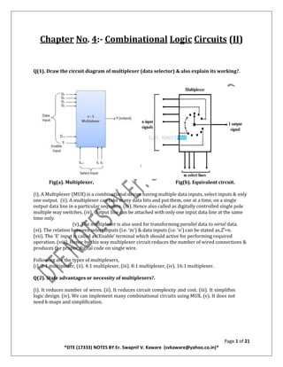
- 1. Page 1 of 21 *DTE (17333) NOTES BY Er. Swapnil V. Kaware (svkaware@yahoo.co.in)* Chapter No. 4:- Combinational Logic Circuits (II) Q(1). Draw the circuit diagram of multiplexer (data selector) & also explain its working?. Fig(a). Multiplexer, Fig(b). Equivalent circuit. (i). A Multiplexer (MUX) is a combinational device having multiple data inputs, select inputs & only one output. (ii). A multiplexer can take many data bits and put them, one at a time, on a single output data line in a particular sequence. (iii). Hence also called as digitally controlled single pole multiple way switches. (iv). Output line can be attached with only one input data line at the same time only. (v). The multiplexer is also used for transforming parallel data to serial data. (vi). The relation between select inputs (i.e. ‘m’) & data inputs (i.e. ‘n’) can be stated as,2 ͫ=n. (vii). The ‘E’ input is called as ‘Enable’ terminal which should active for performing required operation. (viii). Hence by this way multiplexer circuit reduces the number of wired connections & produces the proper digital code on single wire. Following are the types of multiplexers, (i). 2:1 multiplexer, (ii). 4:1 multiplexer, (iii). 8:1 multiplexer, (iv). 16:1 multiplexer. Q(2). State advantages or necessity of multiplexers?. (i). It reduces number of wires. (ii). It reduces circuit complexity and cost. (iii). It simplifies logic design. (iv). We can implement many combinational circuits using MUX. (v). It does not need k-maps and simplification.
- 2. Page 2 of 21 *DTE (17333) NOTES BY Er. Swapnil V. Kaware (svkaware@yahoo.co.in)* Q(3). Draw logic symbol, circuit diagram & truth table of 2:1 multiplexer?. Fig. (a). Logic symbol, Fig.(b). Circuit diagram, Fig.(c). Truth table Q(4). Draw logic symbol, circuit diagram & truth table of 4:1 multiplexer?. Fig. (a). Logic symbol, Fig.(b). Circuit diagram, Fig.(c). Truth table Q(5). Draw logic symbol, circuit diagram & truth table of 8:1 multiplexer?. E S Y 1 0 Io 1 1 I1 E S1 S0 Y 1 0 0 Io 1 0 1 I1 1 1 0 I2 1 1 1 I3 E S2 S1 S0 Y 1 0 0 0 Do 1 0 0 1 D1 1 0 1 0 D2 1 0 1 1 D3 1 1 0 0 D4 1 1 0 1 D5 1 1 1 0 D6 1 1 1 1 D7 S1 S0
- 3. Page 3 of 21 *DTE (17333) NOTES BY Er. Swapnil V. Kaware (svkaware@yahoo.co.in)* (6). Obtain 8:1 multiplexer using two 4:1 multiplexer?. (7). Obtain 16:1 multiplexer using 4:1 multiplexer?.
- 4. Page 4 of 21 *DTE (17333) NOTES BY Er. Swapnil V. Kaware (svkaware@yahoo.co.in)* (8). Obtain 32:1 multiplexer using 8:1 multiplexer?. Q(9). Draw the circuit diagram of demultiplexer & also explain its operation?. (i). A Demultiplexer (DEMUX) is a combinational device having multiple data outputs, select inputs & only one input. (ii). Hence, a demultiplexer can take only data bits and put them, one at a time, on a multiple output data lines in a particular sequence. (iii). Hence also called as digitally controlled multiple pole single way switch. (iv). The Demultiplexer is also used for transforming serial data to parallel data. (v). The relation between select inputs (i.e. ‘m’) & outputs (i.e. ‘n’) can be stated as, 2 ͫ=n. (vi). The E input is called as Probe/Enable terminal which should active for performing required operation. (vii). Hence by this way demultiplexer circuit increases the number of wired connections & produces the proper digital code on multiple wires. Following are the types of demultiplexers, (i). 1:2 demultiplexer, (ii). 1:4 demultiplexer, (iii). 1:8 demultiplexer, (iv). 1:16 demultiplexer.
- 5. Page 5 of 21 *DTE (17333) NOTES BY Er. Swapnil V. Kaware (svkaware@yahoo.co.in)* Fig(a). Multiplexer, Fig(b). Equivalent circuit. Q(10). Draw logic symbol, circuit diagram & truth table of 1:2 demultiplexer?. Fig. (a). Logic symbol, Fig.(b). Circuit diagram, Fig.(c). Truth table E S0 Y1 Y0 1 0 0 Din=1 1 1 Din=1 0
- 6. Page 6 of 21 *DTE (17333) NOTES BY Er. Swapnil V. Kaware (svkaware@yahoo.co.in)* Q(11). Draw logic symbol, circuit diagram & truth table of 1:4 demultiplexer?. Fig. (a). Logic symbol, Fig.(b). Circuit diagram, Q(12). Give/compare differences between Multiplexer & Demultiplxer?. Parameter Multiplexer Demultiplxer (i). No. of data inputs:- n 1 (ii). No. of data outputs:- 1 n (iii). Switch type:- Single pole multiple way Multiple pole single way (iv). Data selector:- Yes No (v). Examples:- 2:1 MUX, 4:1 MUX etc. 1:2 DEMUX, 1:4 DEMUX etc. (vi). Application:- Data selector Data distributor E Din S1 S0 Y0 Y1 Y2 Y3 1 0 0 0 0 0 0 0 1 1 0 0 1 0 0 0 1 0 0 1 0 0 0 0 1 1 0 1 0 1 0 0 1 0 1 0 0 0 0 0 1 1 1 0 0 0 1 0 1 0 1 1 0 0 0 0 1 1 1 1 0 0 0 1 Fig.(c). Truth table
- 7. Page 7 of 21 *DTE (17333) NOTES BY Er. Swapnil V. Kaware (svkaware@yahoo.co.in)* Q(13). Draw logic symbol, circuit diagram & truth table of 1:8 demultiplexer?.
- 8. Page 8 of 21 *DTE (17333) NOTES BY Er. Swapnil V. Kaware (svkaware@yahoo.co.in)* (14). Obtain 1:8 demultiplexer using two 1:4 demultiplexer?. (15). Obtain 1:16 demultiplexer using 1:4 demultiplexer?.
- 9. Page 9 of 21 *DTE (17333) NOTES BY Er. Swapnil V. Kaware (svkaware@yahoo.co.in)* Q(16). What is encoder?. Draw its block diagram?. (i). Digital Encoder is a combinational circuit that generates a specific code at its outputs such as binary or BCD in response to one or more active inputs. (ii). Hence an encoder is a device, circuit, transducer, software program, algorithm or person that converts information from one format or code to another, for the purposes of standardization, speed or compression. (iii). There are two main types of digital encoder. (iv). The Binary Encoder and the Priority Encoder. Q(17). Explain priority encoder with block diagram?. (i). A priority encoder provide n bits of binary coded output representing the position of the highest order active input of 2ninputs. (ii). The priority encoders output corresponds to the currently active input which has the highest priority (iii). If two or more inputs are high at the same time, the input having the highest priority will take precedence. 8-to-3 Bit Priority Encoder:- (iv). Priority encoders output the highest order input first for example, if input lines “D2“, “D3” and “D5” are applied simultaneously the output code would be for input “D5” (“101”) as this has the highest order out of the 3 inputs. (v). Once input “D5” had been removed the next highest output code would be for input “D3” (“011”), and so on. (vi). Where X equals “dont care”, that is logic “0” or a logic “1”.
- 10. Page 10 of 21 *DTE (17333) NOTES BY Er. Swapnil V. Kaware (svkaware@yahoo.co.in)* Output Q0 Output Q1 Output Q2 Then the final Boolean expression for the priority encoder including the zero inputs is defined as: Digital Encoder using Logic Gates
- 11. Page 11 of 21 *DTE (17333) NOTES BY Er. Swapnil V. Kaware (svkaware@yahoo.co.in)* Q(18). Explain decimal to BCD encoder with truth table?. Decimal to BCD Encoder:- (i). This type of encoder usually consists of ten input lines and 4 output lines. (ii). Each input line corresponds to the each decimal digit and 4 outputs correspond to the BCD code. (iii). This encoder accepts the decoded decimal data as an input and encodes it to the BCD output which is available on the output lines. (iv). The figure below shows the basic logic symbol of decimal to BCD encoder along with its truth table. (v). The truth table represents the BCD code for each decimal digit. (vi). From this we can formulate the relationship between the BCD bit and decimal digit. (vii). It is important to note that there is no explicit input line for decimal zero. (viii). When this condition occurs, i.e., decimal inputs 1 to 9 all are zero, then the BCD output is 0000. From the above table, we get the expressions as Y3 = D8 + D9 Y2 = D4 + D5 + D6 + D7 Y1 = D2 + D3 + D6 + D7 Y0 = D1 + D3 + D5 + D7 + D9 From the above expressions, the decimal to BCD encoder logic circuit can be implemented by using set of OR gates as shown in below figure.
- 12. Page 12 of 21 *DTE (17333) NOTES BY Er. Swapnil V. Kaware (svkaware@yahoo.co.in)* Back to top Q(19). Explain Octal to Binary Encoder with truth table?. Octal to Binary Encoder:- (i). An octal to binary encoder consists of eight input lines and three output lines. (ii). Each input line corresponds to each octal digit and three outputs generate corresponding binary code. (iii). In encoders, it is to be assumed that only one input is active or has a value 1 at any given time otherwise the circuit has no meaning. (iv). The figure below shows the logic symbol of octal to binary encoder along with its truth table.
- 13. Page 13 of 21 *DTE (17333) NOTES BY Er. Swapnil V. Kaware (svkaware@yahoo.co.in)* (v). From the above table, the output Y2 becomes 1 if any of the digits D4 or D5 or D6 or D7 is one. Thus, we can write its expression as Y2 = D4 + D5 + D6 + D7 Similarly, Y1 = D2 + D3 + D6 + D7 and Y0 = D1 + D3 + D5 + D7 (vi). Also it is to be observed that D0 does not exist in any of the expressions so it is considered as don’t care. (vii). From the above expressions, we can implement the octal to binary encoder using set of OR gates as shown in figure below. (vii). There is ambiguity in the octal to binary encoder that when all the inputs are zero, an output with all 0’s is generated. (viii). Also, when Do is 1, the output generated is zero. (ix). This is a major problem in this type of encoder. (x). This can be resolved by specifying the condition that none of the inputs are active with an additional output. Q(20). What is decoder?. Explain with equivalent circuit diagram?. DECODERS:- (I). Decoder is a combinational circuit that decodes the data from n input lines to 2^n outputs. (ii). Figure shows the blocks of 2-to-4, 3-to-8 and 4-to-16 decoders. (iii). Here, if three inputs are available in the decoder eight outputs will be available in the decoder which is known as 3-to-8 decoder. (iv). A decoder is a circuit that changes a code into a set of signals. (v). It is called a decoder because it does the reverse of encoding, but we will begin our study of encoders and decoders with decoders because they are simpler to design. (vi). A common type of decoder is the line decoder which takes an n-digit binary number and decodes it into 2ndata lines.
- 14. Page 14 of 21 *DTE (17333) NOTES BY Er. Swapnil V. Kaware (svkaware@yahoo.co.in)* Q(21). Draw the logic symbol, circuit diagram & truth table of 3:8 decoder?. Fig. (a). Logic symbol, Fig.(b). Circuit diagram, Fig.(c). Truth table.
- 15. Page 15 of 21 *DTE (17333) NOTES BY Er. Swapnil V. Kaware (svkaware@yahoo.co.in)* Q(22). Explain BCD to seven segment decoder with neat circuit diagram?. (i). BCD to seven segment decoder is a circuit used to convert the input BCD into a form suitable for the display. (ii). It has four input lines (A, B, C and D) and 7 output lines (a, b, c, d, e, f and g) as shown in Figure 3. (iii). Considering common cathode type of arrangement, the truth table for the decoder can be given as in Table I. (iv). Table I Truth table for common cathode type BCD to seven segment decoder
- 16. Page 16 of 21 *DTE (17333) NOTES BY Er. Swapnil V. Kaware (svkaware@yahoo.co.in)* (v). This table indicates the segments which are to be driven high to obtain certain decimal digit at the output of the seven segment display. (vi). However, it is to be noted that in the case of common anode type, the only change will be to interchange ones and zeros on the table. (vii). This means that from the truth table so obtained one can get to know where low has to be driven so as to obtain the required digit at the output. Q(23). Explain digital comparator with neat circuit diagram?. (i). Digital Comparator:- (i). A magnitude digital comparator is a combinational circuit that compares two digital or binary numbers (consider A and B). (ii). It also determines their relative magnitudes in order to find out whether one number is equal, less than or greater than the other digital number. (iii). Three binary variables are used to indicate the outcome of the comparison as A>B, A<B, or A=B. (iv). The below figure shows the block diagram of a n-bit comparator which compares the two numbers of n-bit length and generates their relation between themselves. (v). These comparators can compare 2-bit, 4-bit and 8-bit numbers depending on the application requirement. (vi). These are available in TTL as well as CMOS logic family ICs and some of these ICs include IC 7485 (4-bit comparator), IC 4585 (4-bit comparator in CMOS family) and IC 74AS885 (8- bit comparator). Q(24). Explain 2-Bit Comparator with neat circuit diagram?. (i). A 2-bit comparator compares two binary numbers, each of two bits and produces their relation such as one number is equal or greater than or less than the other. (ii). The figure below shows the block diagram of a two-bit comparator which has four inputs and three outputs. (iii). The first number A is designated as A = A1A0 and the second number is designated as B = B1B0. (iv). This comparator produces three outputs as G (G = 1 if A>B), E (E = 1, if A = B) and L (L = 1 if A<B).
- 17. Page 17 of 21 *DTE (17333) NOTES BY Er. Swapnil V. Kaware (svkaware@yahoo.co.in)* The truth table of this comparator is shown below which depicting various input and output states. The k-map simplification for the above truth table is as follows.
- 18. Page 18 of 21 *DTE (17333) NOTES BY Er. Swapnil V. Kaware (svkaware@yahoo.co.in)* From the above k-map simplification, each output can be expressed as The figure below shows the logic diagram of a 2-bit comparator using basic logic gates. It is also possible to construct this comparator by cascading of two 1-bit comparators.
- 19. Page 19 of 21 *DTE (17333) NOTES BY Er. Swapnil V. Kaware (svkaware@yahoo.co.in)* Q(25). Explain 4-Bit Comparator with neat circuit diagram?. (i). 4-Bit Comparator:- (i). It can be used to compare two four-bit words. The two 4-bit numbers are A = A3 A2 A1 A0 and B3 B2 B1 B0 where A3 and B3 are the most significant bits. (ii). It compares each of these bits in one number with bits in that of other number and produces one of the following outputs as A = B, A < B and A>B. The output logic statements of this converter are If A3 = 1 and B3 = 0, then A is greater than B (A>B). Or If A3 and B3 are equal, and if A2 = 1 and B2 = 0, then A > B. Or If A3 and B3 are equal & A2 and B2 are equal, and if A1 = 1, and B1 = 0, then A>B. Or If A3 and B3 are equal, A2 and B2 are equal and A1 and B1 are equal, and if A0 = 1 and B0 = 0, then A > B. (iv). From the above statements, the output A > B logic expression can be written as (v). The equal output is produced when all the individual bits of one number are exactly coincides with corresponding bits of another number. (vi). Then the logical expression for A=B output can be written as E = (A3 Ex-NOR B3) (A2 Ex-NOR B2) (A1 Ex-NOR B1) (A0 Ex-NOR B0) (vii). From the above output Boolean expressions, the logic circuit for this comparator can be implemented by using logic gates as given below. (viii). In this the four outputs from Ex-NOR gates are applied to AND gate to give the binary variable E or A = B. (ix). The other two outputs are also use Ex-NOR outputs to generate the Boolean functions as shown figure. (x). The 4-bit comparator is mostly available in IC form and common type of this IC is 7485. (xi). This IC can be used to compare two 4-bit binary words by grounding I (A>B), I (A<B) and I (A=B) connector inputs to Vcc terminal. (xii). In addition to the normal comparator, this IC is provided with cascading inputs in order to facilitate the cascading several comparators. (xiii). Any number of bits can be compared by cascading several of these comparator ICs.
- 20. Page 20 of 21 *DTE (17333) NOTES BY Er. Swapnil V. Kaware (svkaware@yahoo.co.in)* Q(26). Explain 8-Bit Comparator with neat circuit diagram?. (i). 8-Bit Comparator:- (i). An 8-bit comparator compares the two 8-bit numbers by cascading of two 4-bit comparators. (ii). The circuit connection of this comparator is shown below in which the lower order comparator A<B, A=B and A>B outputs are connected to the respective cascade inputs of the higher order comparator. (iii). For the lower order comparator, the A=B cascade input must be connected High, while the other two cascading inputs A ,B must be connected to LOW. (iv). The outputs of the higher order comparator become the outputs of this eight-bit comparator.
- 21. Page 21 of 21 *DTE (17333) NOTES BY Er. Swapnil V. Kaware (svkaware@yahoo.co.in)* Applications of Comparators (i). These are used in the address decoding circuitry in computers and microprocessor based devices to select a specific input/output device for the storage of data. (ii). These are used in control applications in which the binary numbers representing physical variables such as temperature, position, etc. are compared with a reference value. (iii). Then the outputs from the comparator are used to drive the actuators so as to make the physical variables closest to the set or reference value. ***************************************** ALL THE BEST *****************************************