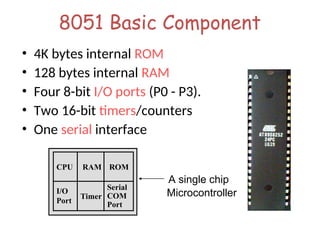
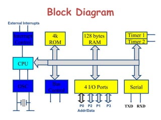
8051 Basic Component
•4K bytes internal ROM
• 128 bytes internal RAM
• Four 8-bit I/O ports (P0 - P3).
• Two 16-bit timers/counters
• One serial interface
RAM
I/O
Port
Timer
Serial
COM
Port
Microcontroller
CPU
A single chip
ROM
Other 8051 featurs
•only 1 On chip oscillator (external crystal)
• 6 interrupt sources (2 external , 3 internal, Reset)
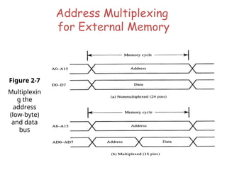
• 64K external code (program) memory(only read)PSEN
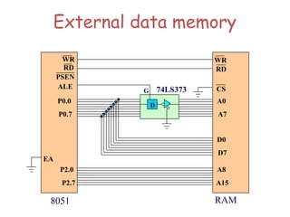
• 64K external data memory(can be read and write) by RD,WR
• Code memory is selectable by EA (internal or external)
• We may have External memory as data and code
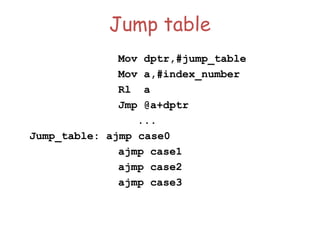
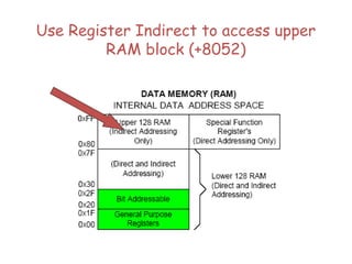
5.
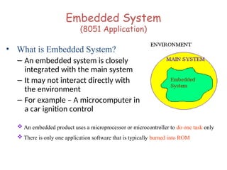
Embedded System
(8051 Application)
•What is Embedded System?
– An embedded system is closely
integrated with the main system
– It may not interact directly with
the environment
– For example – A microcomputer in
a car ignition control
An embedded product uses a microprocessor or microcontroller to do one task only
There is only one application software that is typically burned into ROM
6.
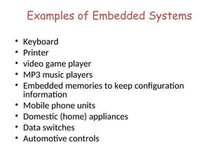
Examples of EmbeddedSystems
• Keyboard
• Printer
• video game player
• MP3 music players
• Embedded memories to keep configuration
information
• Mobile phone units
• Domestic (home) appliances
• Data switches
• Automotive controls
7.
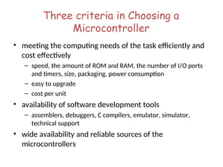
Three criteria inChoosing a
Microcontroller
• meeting the computing needs of the task efficiently and
cost effectively
– speed, the amount of ROM and RAM, the number of I/O ports
and timers, size, packaging, power consumption
– easy to upgrade
– cost per unit
• availability of software development tools
– assemblers, debuggers, C compilers, emulator, simulator,
technical support
• wide availability and reliable sources of the
microcontrollers
8.
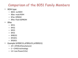
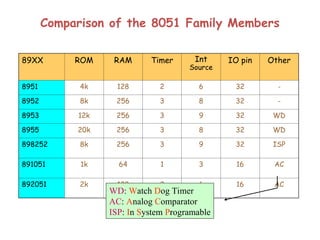
Comparison of the8051 Family Members
• ROM type
– 8031 no ROM
– 80xx mask ROM
– 87xx EPROM
– 89xx Flash EEPROM
• 89xx
– 8951
– 8952
– 8953
– 8955
– 898252
– 891051
– 892051
• Example (AT89C51,AT89LV51,AT89S51)
– AT= ATMEL(Manufacture)
– C = CMOS technology
– LV= Low Power(3.0v)
9.
Comparison of the8051 Family Members
89XX ROM RAM Timer Int
Source
IO pin Other
8951 4k 128 2 6 32 -
8952 8k 256 3 8 32 -
8953 12k 256 3 9 32 WD
8955 20k 256 3 8 32 WD
898252 8k 256 3 9 32 ISP
891051 1k 64 1 3 16 AC
892051 2k 128 2 6 16 AC
WD: Watch Dog Timer
AC: Analog Comparator
ISP: In System Programable
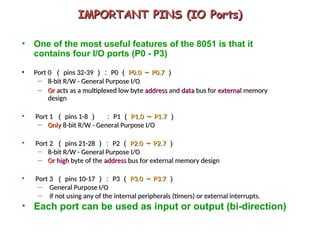
IMPORTANT PINS (IOPorts)
IMPORTANT PINS (IO Ports)
• One of the most useful features of the 8051 is that it
contains four I/O ports (P0 - P3)
• Port 0
Port 0 (
( pins 32-39
pins 32-39 ):
): P0
P0 (
( P0.0
P0.0 ~
~ P0.7
P0.7 )
)
– 8-bit R/W - General Purpose I/O
8-bit R/W - General Purpose I/O
– Or
Or acts as a multiplexed low byte
acts as a multiplexed low byte address
address and
and data
data bus for
bus for external
external memory
memory
design
design
• Port 1
Port 1 (
( pins 1-8
pins 1-8 )
) :
: P1
P1 (
( P1.0
P1.0 ~
~ P1.7
P1.7 )
)
– Only
Only 8-bit R/W - General Purpose I/O
8-bit R/W - General Purpose I/O
• Port 2
Port 2 (
( pins 21-28
pins 21-28 ):
): P2
P2 (
( P2.0
P2.0 ~
~ P2.7
P2.7 )
)
– 8-bit R/W - General Purpose I/O
8-bit R/W - General Purpose I/O
– Or
Or high
high byte of the
byte of the address
address bus for external memory design
bus for external memory design
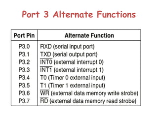
• Port 3
Port 3 (
( pins 10-17
pins 10-17 ):
): P3
P3 (
( P3.0
P3.0 ~
~ P3.7
P3.7 )
)
– General Purpose I/O
General Purpose I/O
– if not using any of the internal peripherals (timers) or external interrupts.
if not using any of the internal peripherals (timers) or external interrupts.
• Each port can be used as input or output (bi-direction)
Port 0 withPull-Up Resistors
P0.0
P0.1
P0.2
P0.3
P0.4
P0.5
P0.6
P0.7
DS5000
8751
8951
Vcc
10 K
Port
0
16.
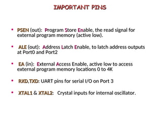
IMPORTANT PINS
IMPORTANT PINS
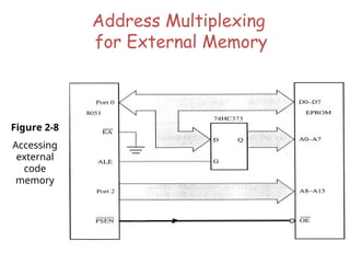
•PSEN
PSEN (out):
(out): P
Program
rogram S
Store
tore En
Enable, the read signal for
able, the read signal for
external program memory (active low).
external program memory (active low).
• ALE
ALE (out):
(out): A
Address
ddress L
Latch
atch E
Enable, to latch address outputs
nable, to latch address outputs
at Port0 and Port2
at Port0 and Port2
• EA
EA (in):
(in): E
External
xternal A
Access Enable, active low to access
ccess Enable, active low to access
external program memory locations 0 to 4K
external program memory locations 0 to 4K
• RXD
RXD,
,TXD
TXD: UART pins for serial I/O on Port 3
: UART pins for serial I/O on Port 3
• XTAL1
XTAL1 &
& XTAL2
XTAL2: Crystal inputs for internal oscillator.
: Crystal inputs for internal oscillator.
17.
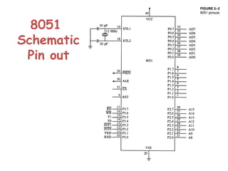
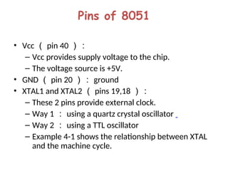
Pins of 8051
•Vcc ( pin 40 ):
– Vcc provides supply voltage to the chip.
– The voltage source is +5V.
• GND ( pin 20 ): ground
• XTAL1 and XTAL2 ( pins 19,18 ):
– These 2 pins provide external clock.
– Way 1 : using a quartz crystal oscillator
– Way 2 : using a TTL oscillator
– Example 4-1 shows the relationship between XTAL
and the machine cycle.
18.
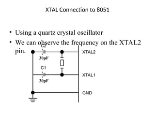
XTAL Connection to8051
• Using a quartz crystal oscillator
• We can observe the frequency on the XTAL2
pin.
C2
30pF
C1
30pF
XTAL2
XTAL1
GND
19.
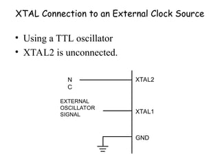
XTAL Connection toan External Clock Source
• Using a TTL oscillator
• XTAL2 is unconnected.
N
C
EXTERNAL
OSCILLATOR
SIGNAL
XTAL2
XTAL1
GND
Pins of 8051
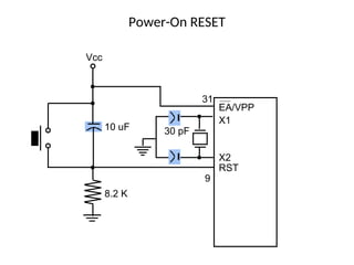
•RST ( pin 9 ): reset
– input pin and active high ( normally low ) .
• The high pulse must be high at least 2 machine
cycles.
– power-on reset.
• Upon applying a high pulse to RST, the
microcontroller will reset and all values in registers
will be lost.
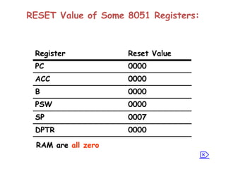
• Reset values of some 8051 registers
– power-on reset circuit
RESET Value ofSome 8051 Registers:
0000
DPTR
0007
SP
0000
PSW
0000
B
0000
ACC
0000
PC
Reset Value
Register
RAM are all zero
24.
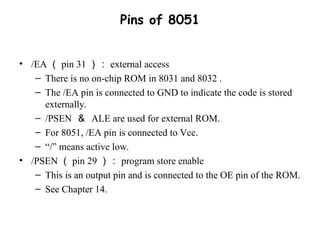
Pins of 8051
•/EA ( pin 31 ): external access
– There is no on-chip ROM in 8031 and 8032 .
– The /EA pin is connected to GND to indicate the code is stored
externally.
– /PSEN & ALE are used for external ROM.
– For 8051, /EA pin is connected to Vcc.
– “/” means active low.
• /PSEN ( pin 29 ): program store enable
– This is an output pin and is connected to the OE pin of the ROM.
– See Chapter 14.
25.
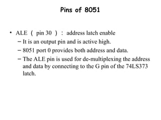
Pins of 8051
•ALE ( pin 30 ): address latch enable
– It is an output pin and is active high.
– 8051 port 0 provides both address and data.
– The ALE pin is used for de-multiplexing the address
and data by connecting to the G pin of the 74LS373
latch.
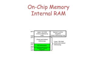
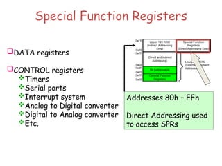
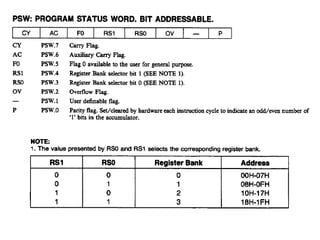
Special Function Registers
DATAregisters
CONTROL registers
Timers
Serial ports
Interrupt system
Analog to Digital converter
Digital to Analog converter
Etc.
Addresses 80h – FFh
Direct Addressing used
to access SPRs
Overview
• Data transferinstructions
• Addressing modes
• Data processing (arithmetic and logic)
• Program flow instructions
42.
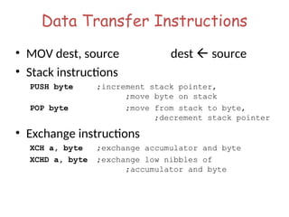
Data Transfer Instructions
•MOV dest, source dest source
• Stack instructions
PUSH byte ;increment stack pointer,
;move byte on stack
POP byte ;move from stack to byte,
;decrement stack pointer
• Exchange instructions
XCH a, byte ;exchange accumulator and byte
XCHD a, byte ;exchange low nibbles of
;accumulator and byte
43.
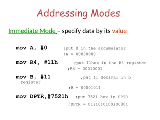
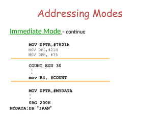
Addressing Modes
Immediate Mode– specify data by its value
mov A, #0 ;put 0 in the accumulator
;A = 00000000
mov R4, #11h ;put 11hex in the R4 register
;R4 = 00010001
mov B, #11 ;put 11 decimal in b
register
;B = 00001011
mov DPTR,#7521h ;put 7521 hex in DPTR
;DPTR = 0111010100100001
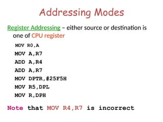
Addressing Modes
Register Addressing– either source or destination is
one of CPU register
MOV R0,A
MOV A,R7
ADD A,R4
ADD A,R7
MOV DPTR,#25F5H
MOV R5,DPL
MOV R,DPH
Note that MOV R4,R7 is incorrect
46.
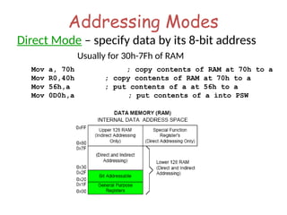
Addressing Modes
Direct Mode– specify data by its 8-bit address
Usually for 30h-7Fh of RAM
Mov a, 70h ; copy contents of RAM at 70h to a
Mov R0,40h ; copy contents of RAM at 70h to a
Mov 56h,a ; put contents of a at 56h to a
Mov 0D0h,a ; put contents of a into PSW
47.
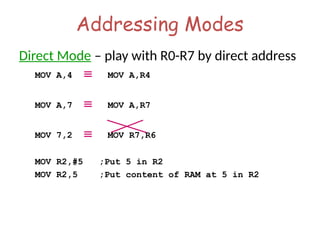
Addressing Modes
Direct Mode– play with R0-R7 by direct address
MOV A,4 MOV A,R4
MOV A,7 MOV A,R7
MOV 7,2 MOV R7,R6
MOV R2,#5 ;Put 5 in R2
MOV R2,5 ;Put content of RAM at 5 in R2
48.
Addressing Modes
Register Indirect– the address of the source or destination is
specified in registers
Uses registers R0 or R1 for 8-bit address:
mov psw, #0 ; use register bank 0
mov r0, #0x3C
mov @r0, #3 ; memory at 3C gets #3
; M[3C] 3
Uses DPTR register for 16-bit addresses:
mov dptr, #0x9000 ; dptr 9000h
movx a, @dptr ; a M[9000]
Note that 9000 is an address in external memory
Addressing Modes
Register IndexedMode – source or destination
address is the sum of the base address and
the accumulator(Index)
• Base address can be DPTR or PC
mov dptr, #4000h
mov a, #5
movc a, @a + dptr ;a M[4005]
51.
Addressing Modes
Register IndexedMode continue
• Base address can be DPTR or PC
ORG 1000h
1000 mov a, #5
1002 movc a, @a + PC ;a M[1008]
1003 Nop
• Table Lookup
• MOVC only can read internal code memory
PC
52.
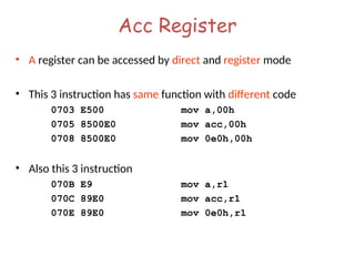
Acc Register
• Aregister can be accessed by direct and register mode
• This 3 instruction has same function with different code
0703 E500 mov a,00h
0705 8500E0 mov acc,00h
0708 8500E0 mov 0e0h,00h
• Also this 3 instruction
070B E9 mov a,r1
070C 89E0 mov acc,r1
070E 89E0 mov 0e0h,r1
53.
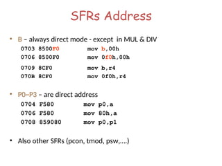
SFRs Address
• B– always direct mode - except in MUL & DIV
0703 8500F0 mov b,00h
0706 8500F0 mov 0f0h,00h
0709 8CF0 mov b,r4
070B 8CF0 mov 0f0h,r4
• P0~P3 – are direct address
0704 F580 mov p0,a
0706 F580 mov 80h,a
0708 859080 mov p0,p1
• Also other SFRs (pcon, tmod, psw,….)
54.
SFRs Address
All SFRssuch as
(ACC, B, PCON, TMOD, PSW, P0~P3, …)
are accessible by name and direct address
But
both of them
Must be coded as direct address
55.
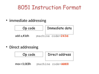
8051 Instruction Format
•immediate addressing
add a,#3dh ;machine code=243d
• Direct addressing
mov r3,0E8h ;machine code=ABE8
Op code Direct address
Op code Immediate data
56.
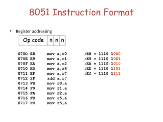
8051 Instruction Format
•Register addressing
070D E8 mov a,r0 ;E8 = 1110 1000
070E E9 mov a,r1 ;E9 = 1110 1001
070F EA mov a,r2 ;EA = 1110 1010
0710 ED mov a,r5 ;ED = 1110 1101
0711 EF mov a,r7 ;Ef = 1110 1111
0712 2F add a,r7
0713 F8 mov r0,a
0714 F9 mov r1,a
0715 FA mov r2,a
0716 FD mov r5,a
0717 FD mov r5,a
Op code n n n
57.
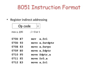
8051 Instruction Format
•Register indirect addressing
mov a, @Ri ; i = 0 or 1
070D E7 mov a,@r1
070D 93 movc a,@a+dptr
070E 83 movc a,@a+pc
070F E0 movx a,@dptr
0710 F0 movx @dptr,a
0711 F2 movx @r0,a
0712 E3 movx a,@r1
Op code i
58.
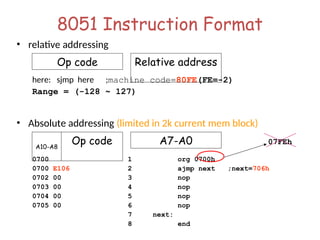
8051 Instruction Format
•relative addressing
here: sjmp here ;machine code=80FE(FE=-2)
Range = (-128 ~ 127)
• Absolute addressing (limited in 2k current mem block)
0700 1 org 0700h
0700 E106 2 ajmp next ;next=706h
0702 00 3 nop
0703 00 4 nop
0704 00 5 nop
0705 00 6 nop
7 next:
8 end
A10-A8
Op code
Op code Relative address
A7-A0 07FEh
59.
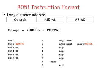
8051 Instruction Format
•Long distance address
Range = (0000h ~ FFFFh)
0700 1 org 0700h
0700 020707 2 ajmp next ;next=0707h
0703 00 3 nop
0704 00 4 nop
0705 00 5 nop
0706 00 6 nop
7 next:
8 end
Op code A15-A8 A7-A0
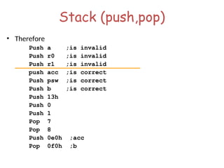
Stack
• Stack-oriented datatransfer
– Only one operand (direct addressing)
– SP is other operand – register indirect - implied
• Direct addressing mode must be used in Push and Pop
mov sp, #0x40 ; Initialize SP
push 0x55 ; SP SP+1, M[SP] M[55]
; M[41] M[55]
pop b ; b M[55]
Note: can only specify RAM or SFRs (direct mode) to push or pop. Therefore,
to push/pop the accumulator, must use acc, not a
Exchange Instructions
two waydata transfer
XCH a, 30h ; a M[30]
XCH a, R0 ; a R0
XCH a, @R0 ; a M[R0]
XCHD a, R0 ; exchange
“digit”
R0[7..4] R0[3..0]
a[7..4] a[3..0]
Only 4 bits exchanged
64.
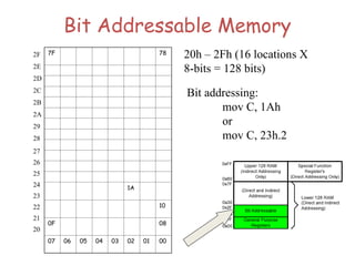
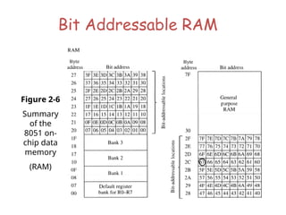
Bit-Oriented Data Transfer
•transfers between individual bits.
• Carry flag (C) (bit 7 in the PSW) is used as a single-bit
accumulator
• RAM bits in addresses 20-2F are bit addressable
mov C, P0.0
mov C, 67h
mov C, 2ch.7
65.
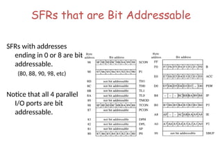
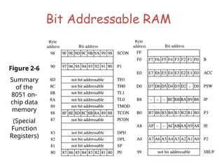
SFRs that areBit Addressable
SFRs with addresses
ending in 0 or 8 are bit-
addressable.
(80, 88, 90, 98, etc)
Notice that all 4 parallel
I/O ports are bit
addressable.
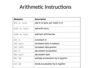
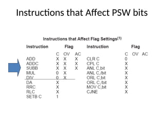
Arithmetic Instructions
Mnemonic Description
ADDA, byte add A to byte, put result in A
ADDC A, byte add with carry
SUBB A, byte subtract with borrow
INC A increment A
INC byte increment byte in memory
INC DPTR increment data pointer
DEC A decrement accumulator
DEC byte decrement byte
MUL AB multiply accumulator by b register
DIV AB divide accumulator by b register
69.
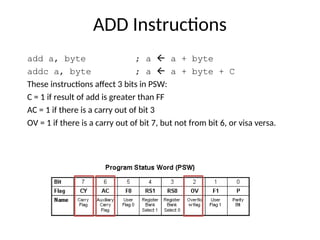
ADD Instructions
add a,byte ; a a + byte
addc a, byte ; a a + byte + C
These instructions affect 3 bits in PSW:
C = 1 if result of add is greater than FF
AC = 1 if there is a carry out of bit 3
OV = 1 if there is a carry out of bit 7, but not from bit 6, or visa versa.
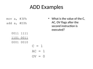
ADD Examples
mov a,#3Fh
add a, #D3h
• What is the value of the C,
AC, OV flags after the
second instruction is
executed?
0011 1111
1101 0011
0001 0010
C = 1
AC = 1
OV = 0
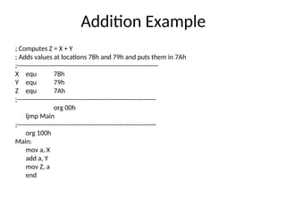
Addition Example
; ComputesZ = X + Y
; Adds values at locations 78h and 79h and puts them in 7Ah
;------------------------------------------------------------------
X equ 78h
Y equ 79h
Z equ 7Ah
;-----------------------------------------------------------------
org 00h
ljmp Main
;-----------------------------------------------------------------
org 100h
Main:
mov a, X
add a, Y
mov Z, a
end
74.
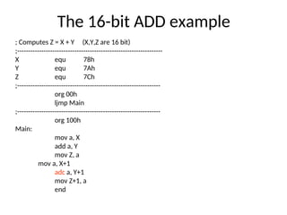
The 16-bit ADDexample
; Computes Z = X + Y (X,Y,Z are 16 bit)
;------------------------------------------------------------------
X equ 78h
Y equ 7Ah
Z equ 7Ch
;-----------------------------------------------------------------
org 00h
ljmp Main
;-----------------------------------------------------------------
org 100h
Main:
mov a, X
add a, Y
mov Z, a
mov a, X+1
adc a, Y+1
mov Z+1, a
end
75.
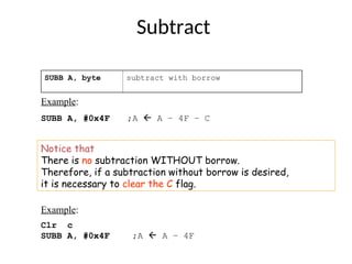
Subtract
SUBB A, bytesubtract with borrow
Example:
SUBB A, #0x4F ;A A – 4F – C
Notice that
There is no subtraction WITHOUT borrow.
Therefore, if a subtraction without borrow is desired,
it is necessary to clear the C flag.
Example:
Clr c
SUBB A, #0x4F ;A A – 4F
76.
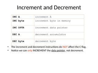
Increment and Decrement
•The increment and decrement instructions do NOT affect the C flag.
• Notice we can only INCREMENT the data pointer, not decrement.
INC A increment A
INC byte increment byte in memory
INC DPTR increment data pointer
DEC A decrement accumulator
DEC byte decrement byte
77.
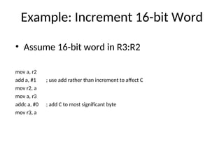
Example: Increment 16-bitWord
• Assume 16-bit word in R3:R2
mov a, r2
add a, #1 ; use add rather than increment to affect C
mov r2, a
mov a, r3
addc a, #0 ; add C to most significant byte
mov r3, a
78.
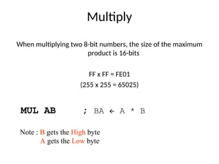
Multiply
When multiplying two8-bit numbers, the size of the maximum
product is 16-bits
FF x FF = FE01
(255 x 255 = 65025)
MUL AB ; BA A * B
Note : B gets the High byte
A gets the Low byte
79.
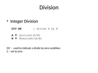
Division
• Integer Division
DIVAB ; divide A by B
A Quotient(A/B)
B Remainder(A/B)
OV - used to indicate a divide by zero condition.
C – set to zero
80.
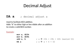
Decimal Adjust
DA a; decimal adjust a
Used to facilitate BCD addition.
Adds “6” to either high or low nibble after an addition
to create a valid BCD number.
Example:
mov a, #23h
mov b, #29h
add a, b ; a 23h + 29h = 4Ch (wanted 52)
DA a ; a a + 6 = 52
81.
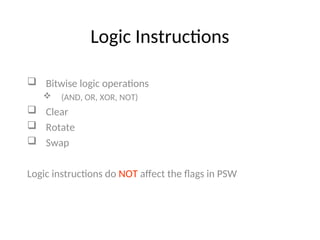
Logic Instructions
Bitwiselogic operations
(AND, OR, XOR, NOT)
Clear
Rotate
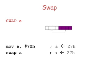
Swap
Logic instructions do NOT affect the flags in PSW
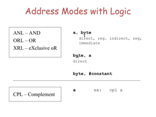
Address Modes withLogic
a, byte
direct, reg. indirect, reg,
immediate
byte, a
direct
byte, #constant
a ex: cpl a
ANL – AND
ORL – OR
XRL – eXclusive oR
CPL – Complement
84.
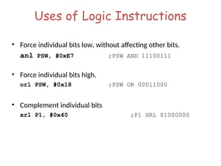
Uses of LogicInstructions
• Force individual bits low, without affecting other bits.
anl PSW, #0xE7 ;PSW AND 11100111
• Force individual bits high.
orl PSW, #0x18 ;PSW OR 00011000
• Complement individual bits
xrl P1, #0x40 ;P1 XRL 01000000
85.
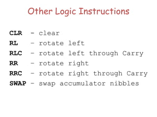
Other Logic Instructions
CLR- clear
RL – rotate left
RLC – rotate left through Carry
RR – rotate right
RRC – rotate right through Carry
SWAP – swap accumulator nibbles
86.
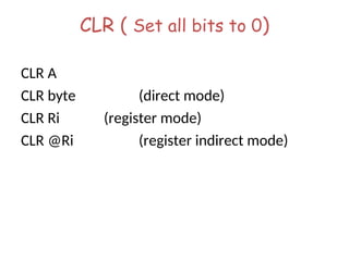
CLR ( Setall bits to 0)
CLR A
CLR byte (direct mode)
CLR Ri (register mode)
CLR @Ri (register indirect mode)
87.
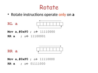
Rotate
• Rotate instructionsoperate only on a
RL a
Mov a,#0xF0 ; a 11110000
RR a ; a 11100001
RR a
Mov a,#0xF0 ; a 11110000
RR a ; a 01111000
88.
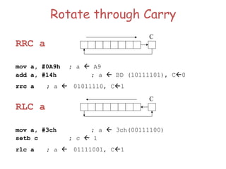
Rotate through Carry
RRCa
mov a, #0A9h ; a A9
add a, #14h ; a BD (10111101), C0
rrc a ; a 01011110, C1
RLC a
mov a, #3ch ; a 3ch(00111100)
setb c ; c 1
rlc a ; a 01111001, C1
C
C
89.
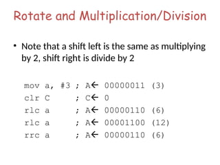
Rotate and Multiplication/Division
•Note that a shift left is the same as multiplying
by 2, shift right is divide by 2
mov a, #3 ; A 00000011 (3)
clr C ; C 0
rlc a ; A 00000110 (6)
rlc a ; A 00001100 (12)
rrc a ; A 00000110 (6)
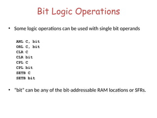
Bit Logic Operations
•Some logic operations can be used with single bit operands
ANL C, bit
ORL C, bit
CLR C
CLR bit
CPL C
CPL bit
SETB C
SETB bit
• “bit” can be any of the bit-addressable RAM locations or SFRs.
Program Flow Control
•Unconditional jumps (“go to”)
• Conditional jumps
• Call and return
94.
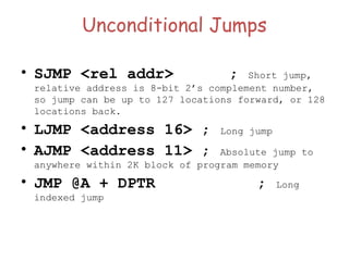
Unconditional Jumps
• SJMP<rel addr> ; Short jump,
relative address is 8-bit 2’s complement number,
so jump can be up to 127 locations forward, or 128
locations back.
• LJMP <address 16> ; Long jump
• AJMP <address 11> ; Absolute jump to
anywhere within 2K block of program memory
• JMP @A + DPTR ; Long
indexed jump
95.
Infinite Loops
Start: movC, p3.7
mov p1.6, C
sjmp Start
Microcontroller application programs are almost always infinite loops!
96.
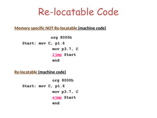
Re-locatable Code
Memory specificNOT Re-locatable (machine code)
org 8000h
Start: mov C, p1.6
mov p3.7, C
ljmp Start
end
Re-locatable (machine code)
org 8000h
Start: mov C, p1.6
mov p3.7, C
sjmp Start
end
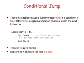
Conditional Jump
• Theseinstructions cause a jump to occur only if a condition is
true. Otherwise, program execution continues with the next
instruction.
loop: mov a, P1
jz loop ; if a=0, goto loop,
; else goto next instruction
mov b, a
• There is no zero flag (z)
• Content of A checked for zero on time
99.
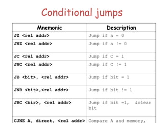
Conditional jumps
Mnemonic Description
JZ<rel addr> Jump if a = 0
JNZ <rel addr> Jump if a != 0
JC <rel addr> Jump if C = 1
JNC <rel addr> Jump if C != 1
JB <bit>, <rel addr> Jump if bit = 1
JNB <bit>,<rel addr> Jump if bit != 1
JBC <bir>, <rel addr> Jump if bit =1, &clear
bit
CJNE A, direct, <rel addr> Compare A and memory,
100.
Example: Conditional Jumps
jzled_off
Setb P1.6
sjmp skipover
led_off: clr P1.6
mov A, P0
skipover:
if (a = 0) is true
send a 0 to LED
else
send a 1 to LED
101.
More Conditional Jumps
MnemonicDescription
CJNE A, #data <rel addr> Compare A and data, jump
if not equal
CJNE Rn, #data <rel addr> Compare Rn and data,
jump if not equal
CJNE @Rn, #data <rel addr> Compare Rn and memory,
jump if not equal
DJNZ Rn, <rel addr> Decrement Rn and then
jump if not zero
102.
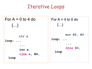
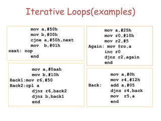
Iterative Loops
For A= 0 to 4 do
{…}
clr a
loop: ...
...
inc a
cjne a, #4,
loop
For A = 4 to 0 do
{…}
mov R0, #4
loop: ...
...
djnz R0,
loop
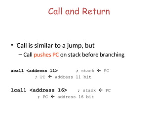
Call and Return
•Call is similar to a jump, but
– Call pushes PC on stack before branching
acall <address ll> ; stack PC
; PC address 11 bit
lcall <address 16> ; stack PC
; PC address 16 bit
105.
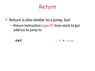
Return
• Return isalso similar to a jump, but
– Return instruction pops PC from stack to get
address to jump to
ret ; PC stack
Initializing Stack Pointer
•SP is initialized to 07 after reset.(Same address as R7)
• With each push operation 1st
, pc is increased
• When using subroutines, the stack will be used to store the PC, so it is
very important to initialize the stack pointer. Location 2Fh is often used.
mov SP, #2Fh
108.
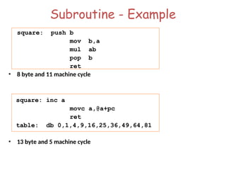
Subroutine - Example
square:push b
mov b,a
mul ab
pop b
ret
• 8 byte and 11 machine cycle
square: inc a
movc a,@a+pc
ret
table: db 0,1,4,9,16,25,36,49,64,81
• 13 byte and 5 machine cycle
109.
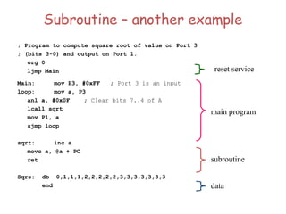
Subroutine – anotherexample
; Program to compute square root of value on Port 3
; (bits 3-0) and output on Port 1.
org 0
ljmp Main
Main: mov P3, #0xFF ; Port 3 is an input
loop: mov a, P3
anl a, #0x0F ; Clear bits 7..4 of A
lcall sqrt
mov P1, a
sjmp loop
sqrt: inc a
movc a, @a + PC
ret
Sqrs: db 0,1,1,1,2,2,2,2,2,3,3,3,3,3,3,3
end
reset service
main program
subroutine
data
110.
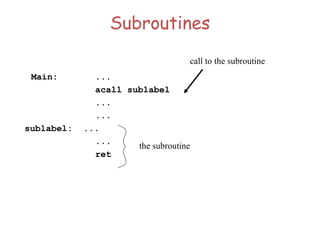
Why Subroutines?
• Subroutinesallow us to have "structured"
assembly language programs.
• This is useful for breaking a large design into
manageable parts.
• It saves code space when subroutines can be
called many times in the same program.
111.
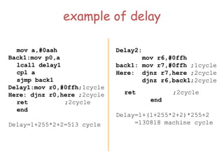
example of delay
mova,#0aah
Back1:mov p0,a
lcall delay1
cpl a
sjmp back1
Delay1:mov r0,#0ffh;1cycle
Here: djnz r0,here ;2cycle
ret ;2cycle
end
Delay=1+255*2+2=513 cycle
Delay2:
mov r6,#0ffh
back1: mov r7,#0ffh ;1cycle
Here: djnz r7,here ;2cycle
djnz r6,back1;2cycle
ret ;2cycle
end
Delay=1+(1+255*2+2)*255+2
=130818 machine cycle
112.
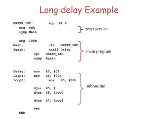
Long delay Example
GREEN_LED:equ P1.6
org ooh
ljmp Main
org 100h
Main: clr GREEN_LED
Again: acall Delay
cpl GREEN_LED
sjmp Again
Delay: mov R7, #02
Loop1: mov R6, #00h
Loop0: mov R5, #00h
djnz R5, $
djnz R6, Loop0
djnz R7, Loop1
ret
END
reset service
main program
subroutine
113.
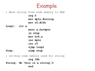
Example
; Move stringfrom code memory to RAM
org 0
mov dptr,#string
mov r0,#10h
Loop1: clr a
movc a,@a+dptr
jz stop
mov @r0,a
inc dptr
inc r0
sjmp loop1
Stop: sjmp stop
; on-chip code memory used for string
org 18h
String: db ‘this is a string’,0
end
114.
Example
; p0:input p1:output
mova,#0ffh
mov p0,a
back: mov a,p0
mov p1,a
sjmp back
setb p1.2
mov a,#45h ;data
Again: jnb p1.2,again ;wait for data
request
mov p0,a ;enable strobe
setb p2.3
clr p2.3
115.
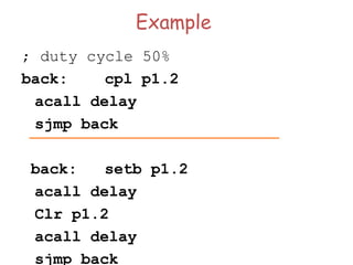
Example
; duty cycle50%
back: cpl p1.2
acall delay
sjmp back
back: setb p1.2
acall delay
Clr p1.2
acall delay
sjmp back
116.
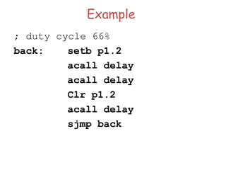
Example
; duty cycle66%
back: setb p1.2
acall delay
acall delay
Clr p1.2
acall delay
sjmp back
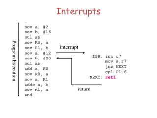
Interrupts
…
mov a, #2
movb, #16
mul ab
mov R0, a
mov R1, b
mov a, #12
mov b, #20
mul ab
add a, R0
mov R0, a
mov a, R1
addc a, b
mov R1, a
end
Program
Execution
interrupt
ISR: inc r7
mov a,r7
jnz NEXT
cpl P1.6
NEXT: reti
return
119.
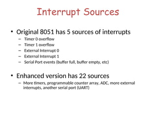
Interrupt Sources
• Original8051 has 5 sources of interrupts
– Timer 0 overflow
– Timer 1 overflow
– External Interrupt 0
– External Interrupt 1
– Serial Port events (buffer full, buffer empty, etc)
• Enhanced version has 22 sources
– More timers, programmable counter array, ADC, more external
interrupts, another serial port (UART)
120.
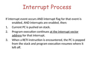
Interrupt Process
If interruptevent occurs AND interrupt flag for that event is
enabled, AND interrupts are enabled, then:
1. Current PC is pushed on stack.
2. Program execution continues at the interrupt vector
address for that interrupt.
3. When a RETI instruction is encountered, the PC is popped
from the stack and program execution resumes where it
left off.
121.
Interrupt Priorities
• Whatif two interrupt sources interrupt at the
same time?
• The interrupt with the highest PRIORITY gets
serviced first.
• All interrupts have a default priority order.
• Priority can also be set to “high” or “low”.
122.
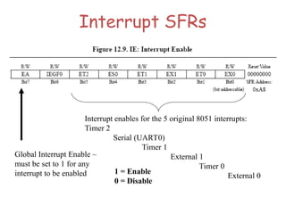
Interrupt SFRs
Global InterruptEnable –
must be set to 1 for any
interrupt to be enabled
Interrupt enables for the 5 original 8051 interrupts:
Timer 2
Serial (UART0)
Timer 1
External 1
Timer 0
External 0
1 = Enable
0 = Disable
123.
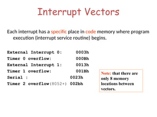
Interrupt Vectors
Each interrupthas a specific place in code memory where program
execution (interrupt service routine) begins.
External Interrupt 0: 0003h
Timer 0 overflow: 000Bh
External Interrupt 1: 0013h
Timer 1 overflow: 001Bh
Serial : 0023h
Timer 2 overflow(8052+) 002bh
Note: that there are
only 8 memory
locations between
vectors.
124.
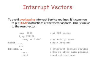
Interrupt Vectors
To avoidoverlapping Interrupt Service routines, it is common
to put JUMP instructions at the vector address. This is similar
to the reset vector.
org 009B ; at EX7 vector
ljmp EX7ISR
cseg at 0x100 ; at Main program
Main: ... ; Main program
...
EX7ISR:... ; Interrupt service routine
... ; Can go after main program
reti ; and subroutines.
125.
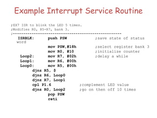
Example Interrupt ServiceRoutine
;EX7 ISR to blink the LED 5 times.
;Modifies R0, R5-R7, bank 3.
;----------------------------------------------------
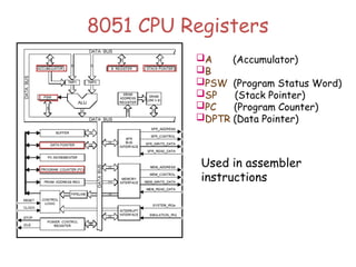
ISRBLK: push PSW ;save state of status
word
mov PSW,#18h ;select register bank 3
mov R0, #10 ;initialize counter
Loop2: mov R7, #02h ;delay a while
Loop1: mov R6, #00h
Loop0: mov R5, #00h
djnz R5, $
djnz R6, Loop0
djnz R7, Loop1
cpl P1.6 ;complement LED value
djnz R0, Loop2 ;go on then off 10 times
pop PSW
reti


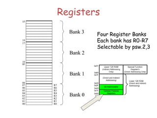
![ Active bank selected by PSW [RS1,RS0] bit
Permits fast “context switching” in interrupt
service routines (ISR).
Register Banks](https://image.slidesharecdn.com/8051-microcontroller-250627032249-3fa361d5/85/8051-MICROCONTROLLER-all-contents-with-diagram-ppt-36-320.jpg)

![Addressing Modes
Register Indirect – the address of the source or destination is
specified in registers
Uses registers R0 or R1 for 8-bit address:
mov psw, #0 ; use register bank 0
mov r0, #0x3C
mov @r0, #3 ; memory at 3C gets #3
; M[3C] 3
Uses DPTR register for 16-bit addresses:
mov dptr, #0x9000 ; dptr 9000h
movx a, @dptr ; a M[9000]
Note that 9000 is an address in external memory](https://image.slidesharecdn.com/8051-microcontroller-250627032249-3fa361d5/85/8051-MICROCONTROLLER-all-contents-with-diagram-ppt-48-320.jpg)
![Addressing Modes
Register Indexed Mode – source or destination
address is the sum of the base address and
the accumulator(Index)
• Base address can be DPTR or PC
mov dptr, #4000h
mov a, #5
movc a, @a + dptr ;a M[4005]](https://image.slidesharecdn.com/8051-microcontroller-250627032249-3fa361d5/85/8051-MICROCONTROLLER-all-contents-with-diagram-ppt-50-320.jpg)
![Addressing Modes
Register Indexed Mode continue
• Base address can be DPTR or PC
ORG 1000h
1000 mov a, #5
1002 movc a, @a + PC ;a M[1008]
1003 Nop
• Table Lookup
• MOVC only can read internal code memory
PC](https://image.slidesharecdn.com/8051-microcontroller-250627032249-3fa361d5/85/8051-MICROCONTROLLER-all-contents-with-diagram-ppt-51-320.jpg)

![Stack
• Stack-oriented data transfer
– Only one operand (direct addressing)
– SP is other operand – register indirect - implied
• Direct addressing mode must be used in Push and Pop
mov sp, #0x40 ; Initialize SP
push 0x55 ; SP SP+1, M[SP] M[55]
; M[41] M[55]
pop b ; b M[55]
Note: can only specify RAM or SFRs (direct mode) to push or pop. Therefore,
to push/pop the accumulator, must use acc, not a](https://image.slidesharecdn.com/8051-microcontroller-250627032249-3fa361d5/85/8051-MICROCONTROLLER-all-contents-with-diagram-ppt-61-320.jpg)
![Exchange Instructions
two way data transfer
XCH a, 30h ; a M[30]
XCH a, R0 ; a R0
XCH a, @R0 ; a M[R0]
XCHD a, R0 ; exchange
“digit”
R0[7..4] R0[3..0]
a[7..4] a[3..0]
Only 4 bits exchanged](https://image.slidesharecdn.com/8051-microcontroller-250627032249-3fa361d5/85/8051-MICROCONTROLLER-all-contents-with-diagram-ppt-63-320.jpg)