Download to read offline

![VOLTAGE DIVIDER BIAS METHOD
Circuit Analysis:
1. 𝐼𝑐
2. 𝑉𝐶𝐸
Collector Current IC:
I1 =VCC ̸ R1+ R2
So, voltage across resistance R2 is
V2 = (VCC ̸ R1+ R2) R2
Appling KVL to the base circuit of the Fig
V2 = VBE + VE
or, V2 = VBE + IERE
or, IE = (V2 - VBE) ̸ RE
Since, IE ≈ IC
∴ IC = (V2 - VBE) ̸ RE
Though IC depends upon VEE but in practice
V2 >> VBE, so that IC is practically
independent of VBE.
Collector-emitter voltage VCE:
Applying KVL to the collector side.
VCC = ICRC + VCE + IERE
= ICRC + VCE + ICRE [Because
IE = IC]
= IC (RC + RE) + VCE
VCE = VCC – IC (RC + RE)](https://image.slidesharecdn.com/mechanism-of2-170909183845/75/Mechanism-of-Electronics-Devices-6-2048.jpg)


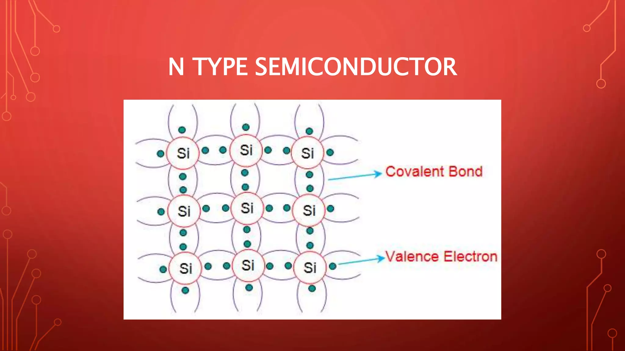
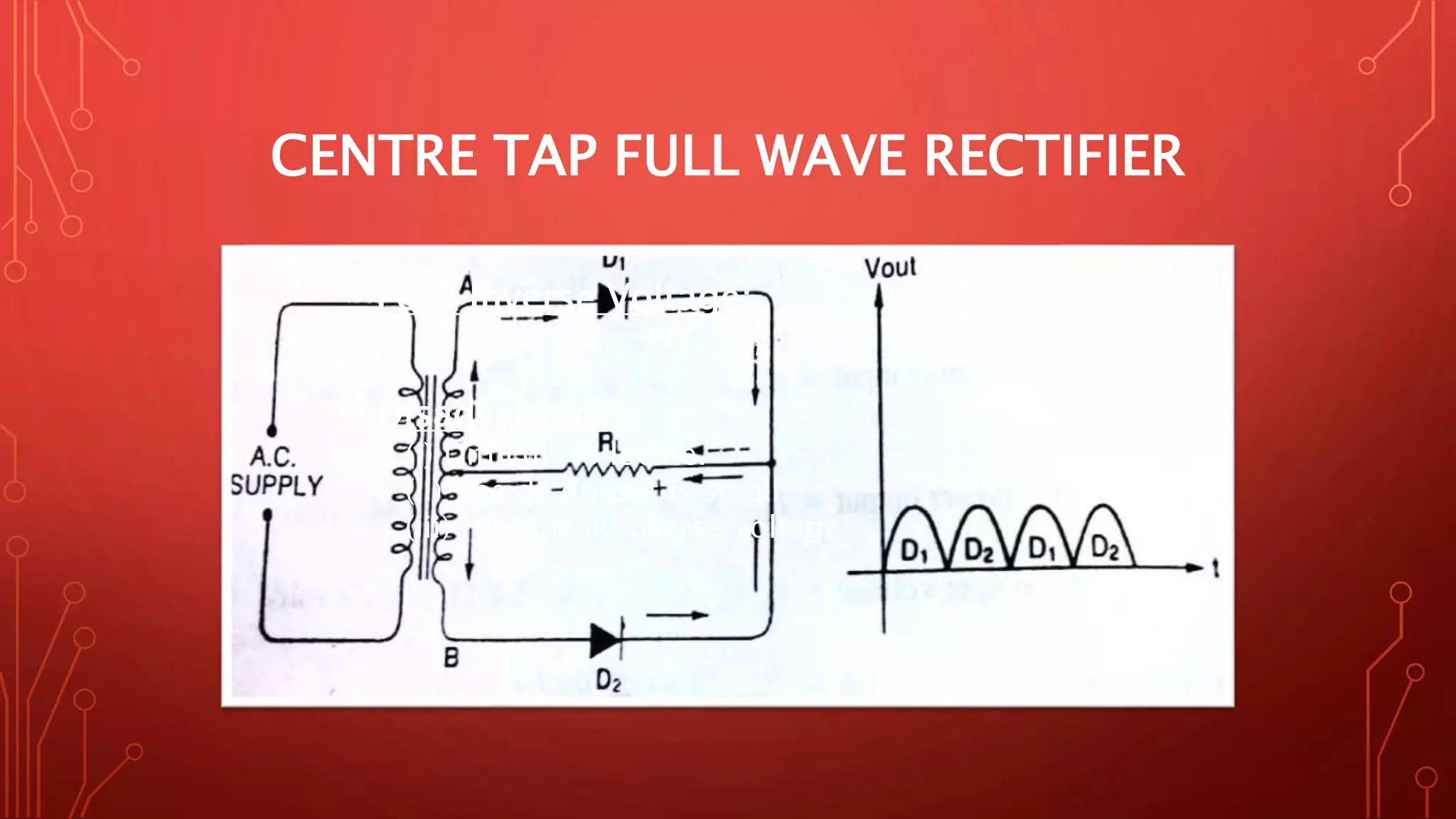
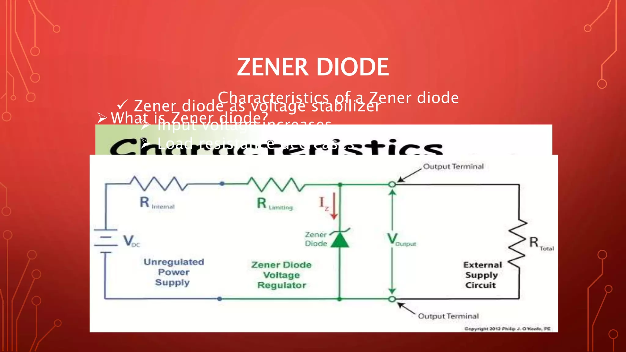
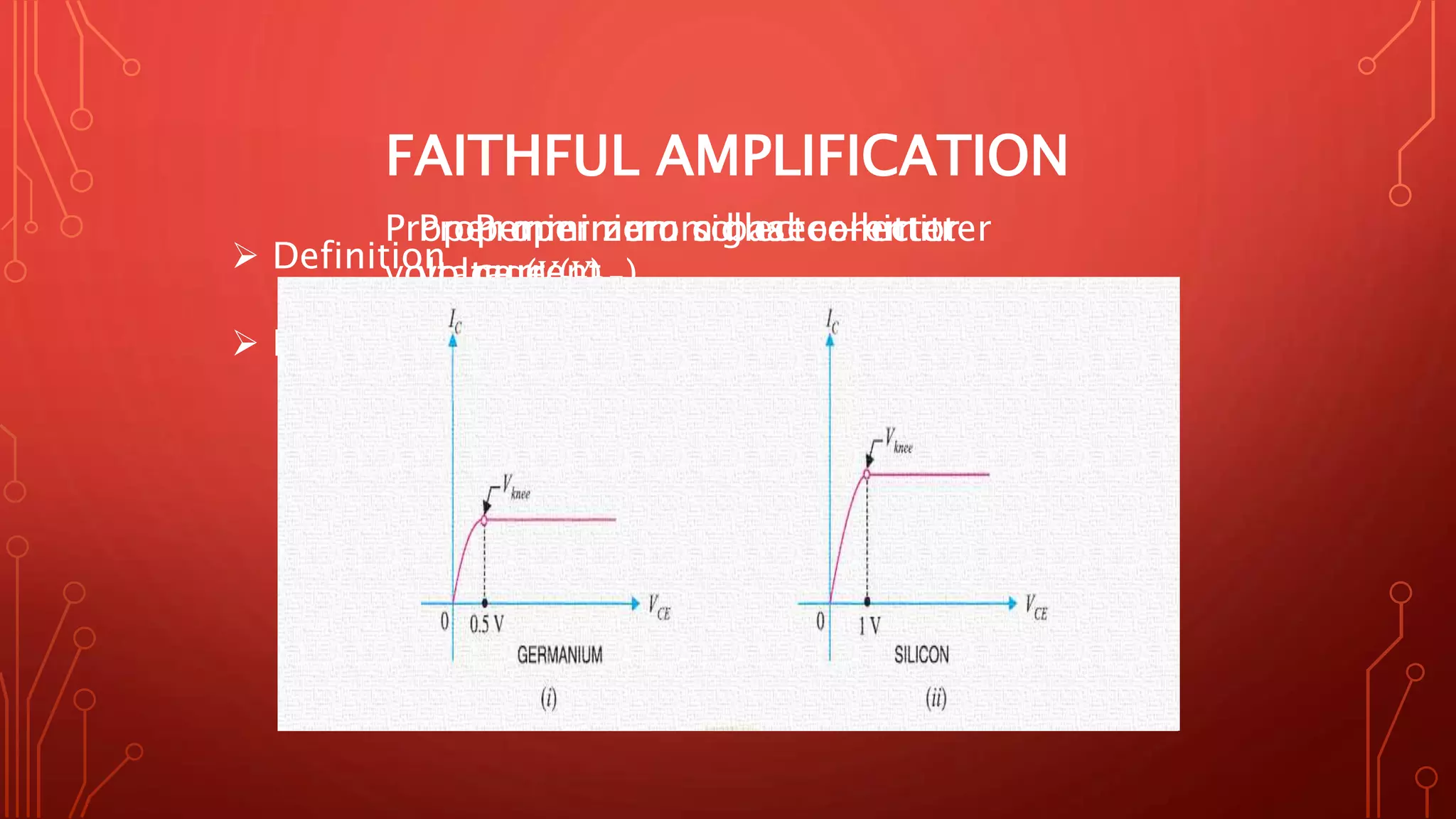
This document discusses several electronic devices and circuits. It describes N-type semiconductors and center tap full wave rectifiers. It also explains zener diodes, their equivalent circuit and characteristics when used for voltage stabilization. The concepts of faithful amplification and proper biasing conditions for transistors are introduced. Specifically, the voltage divider bias method is analyzed, showing calculations for collector current and collector-emitter voltage.