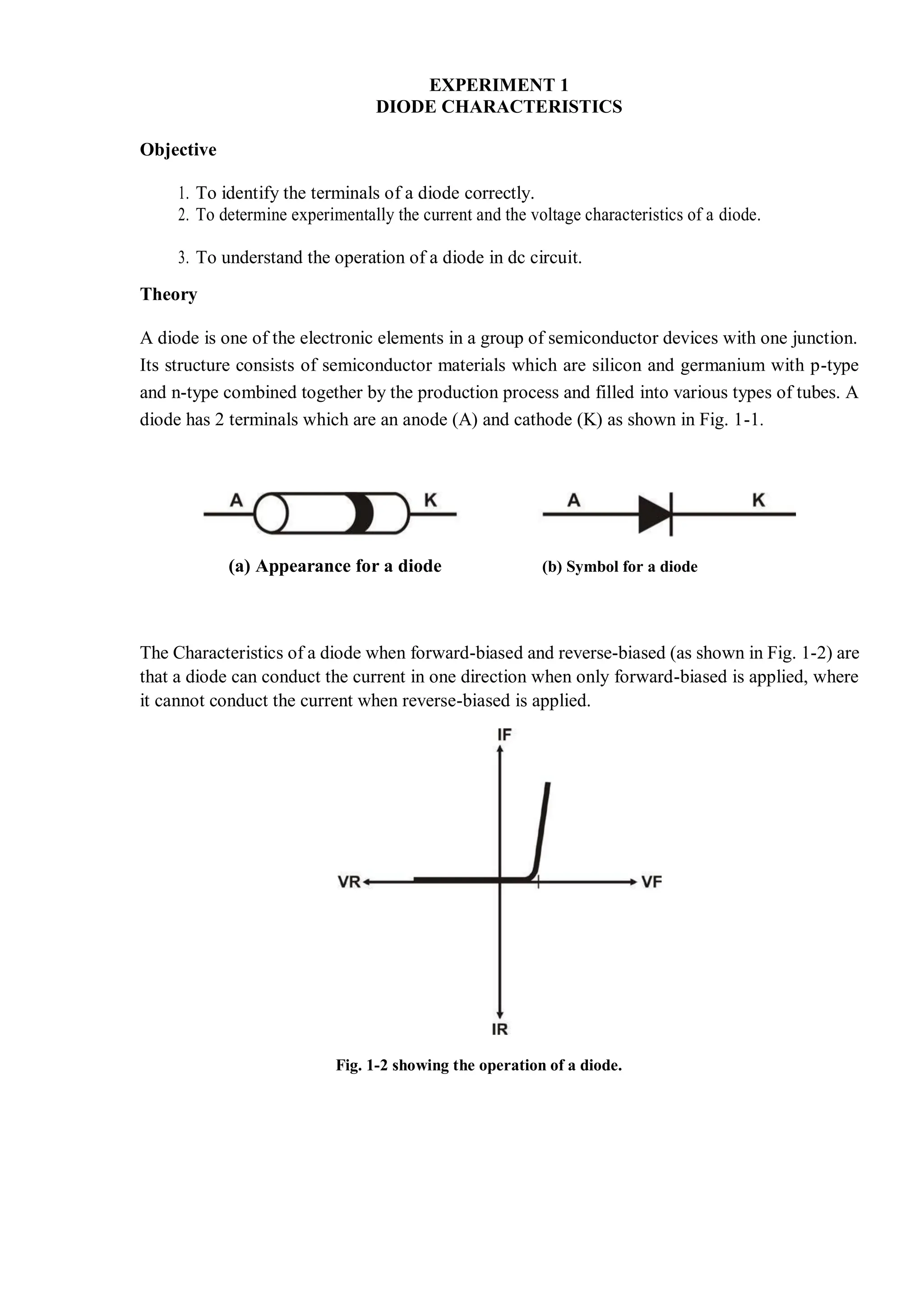
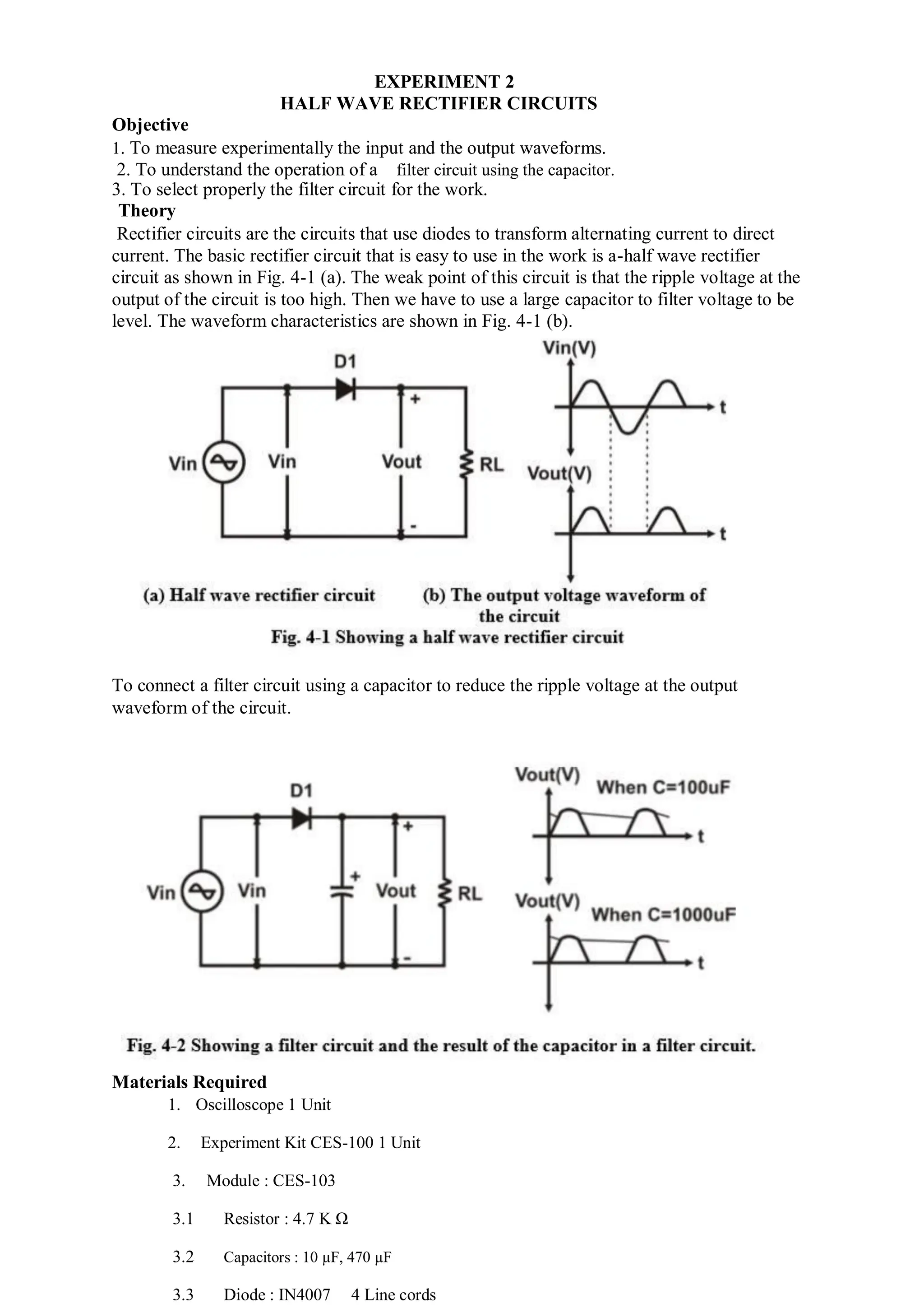
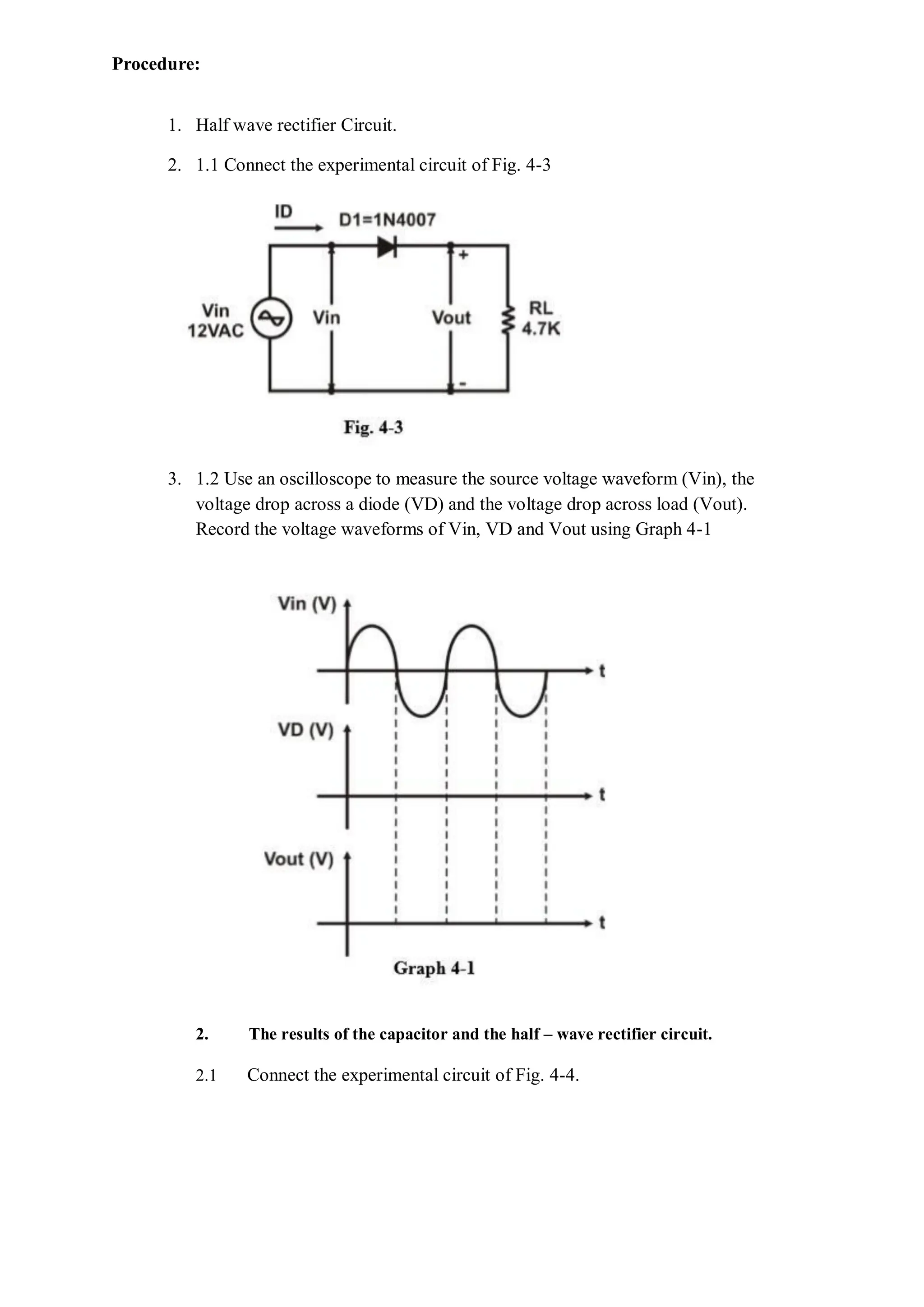
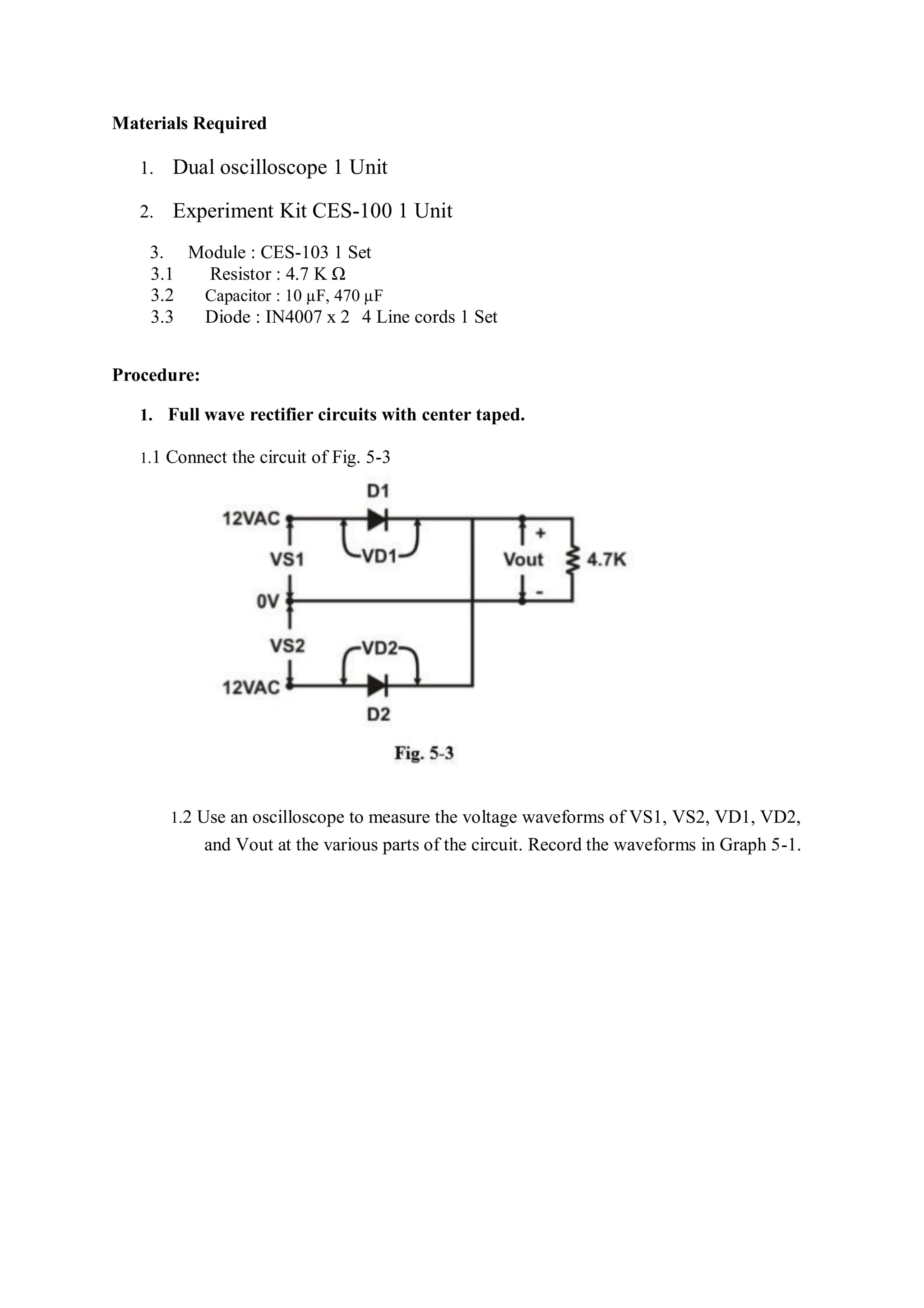
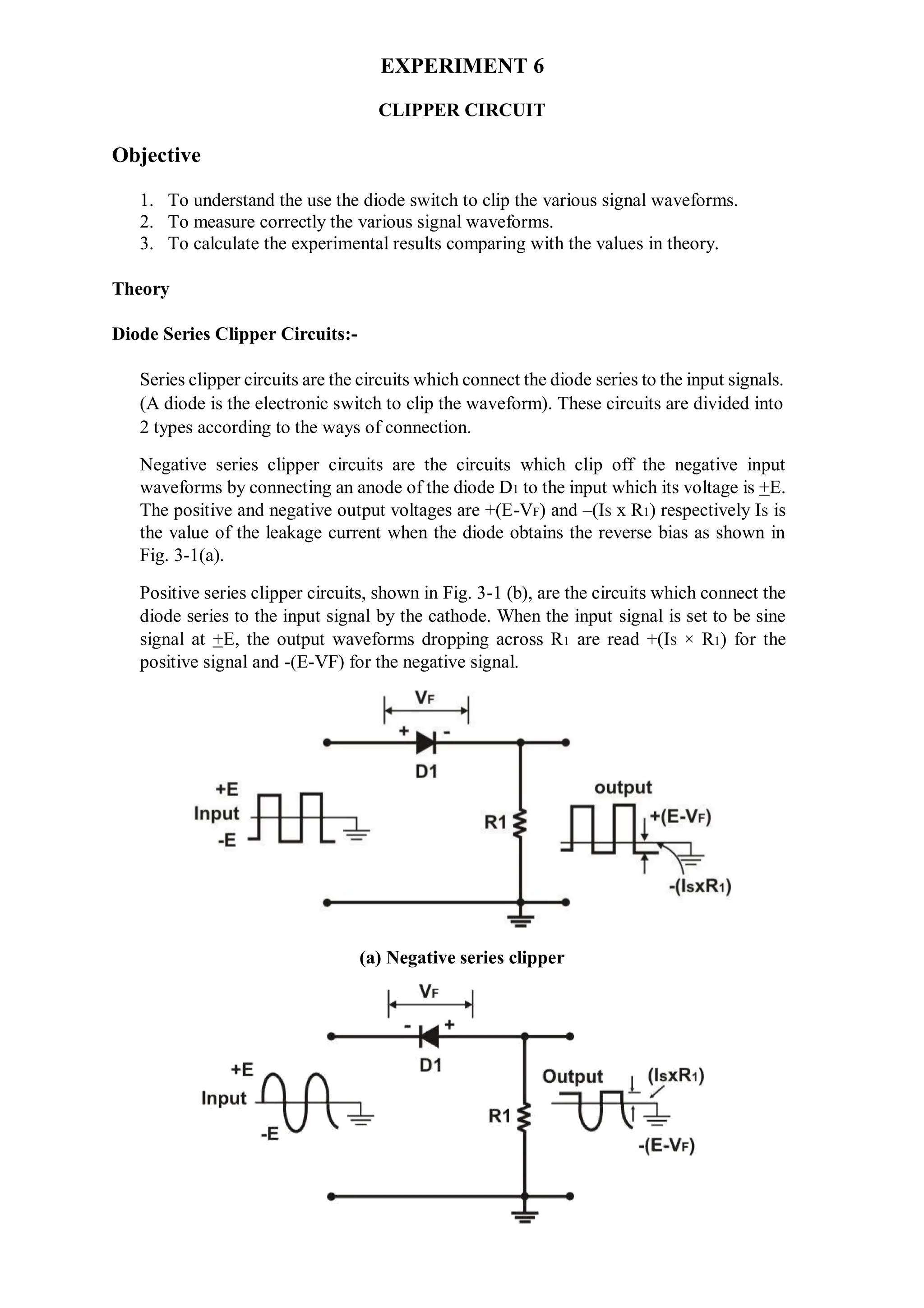
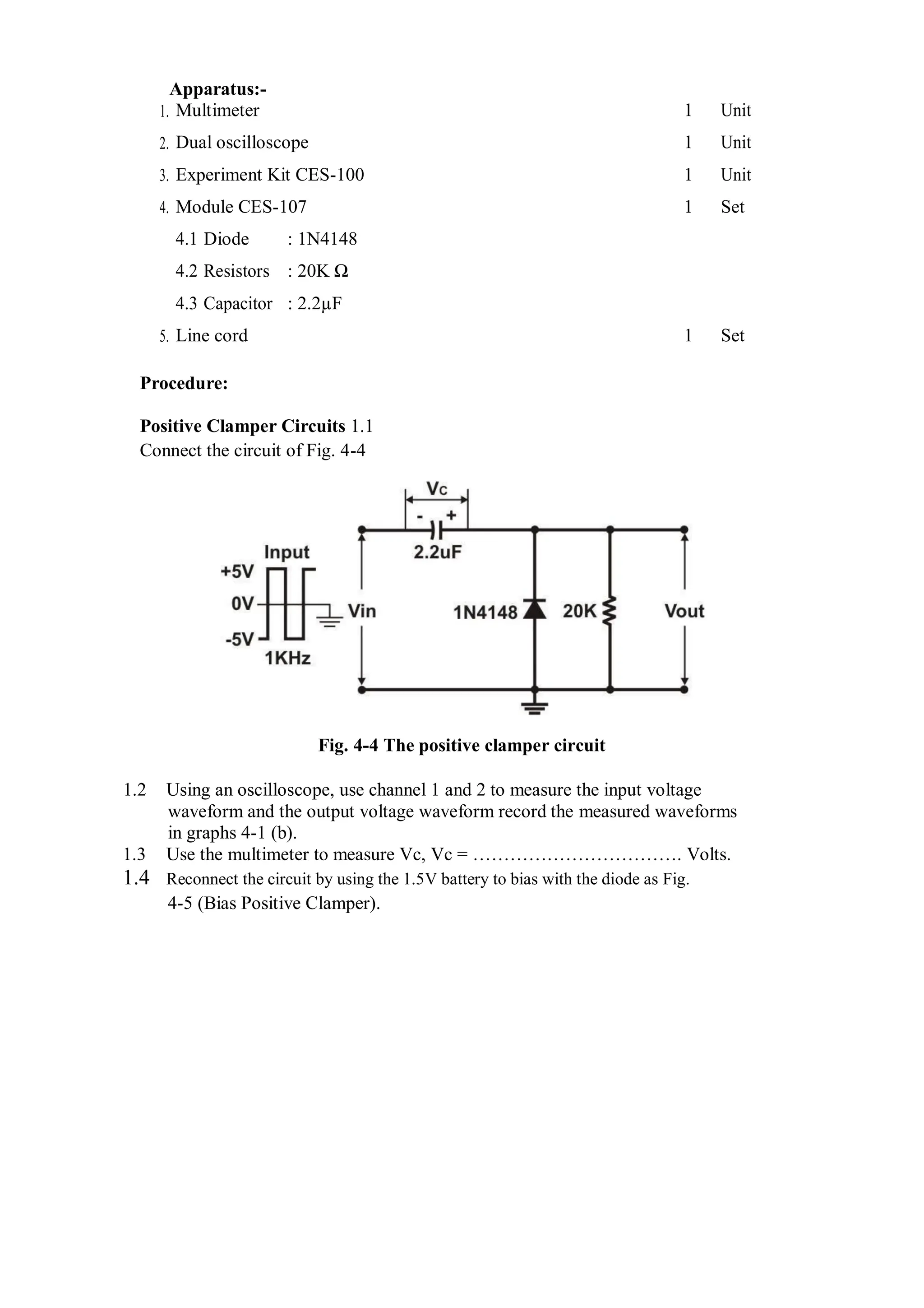
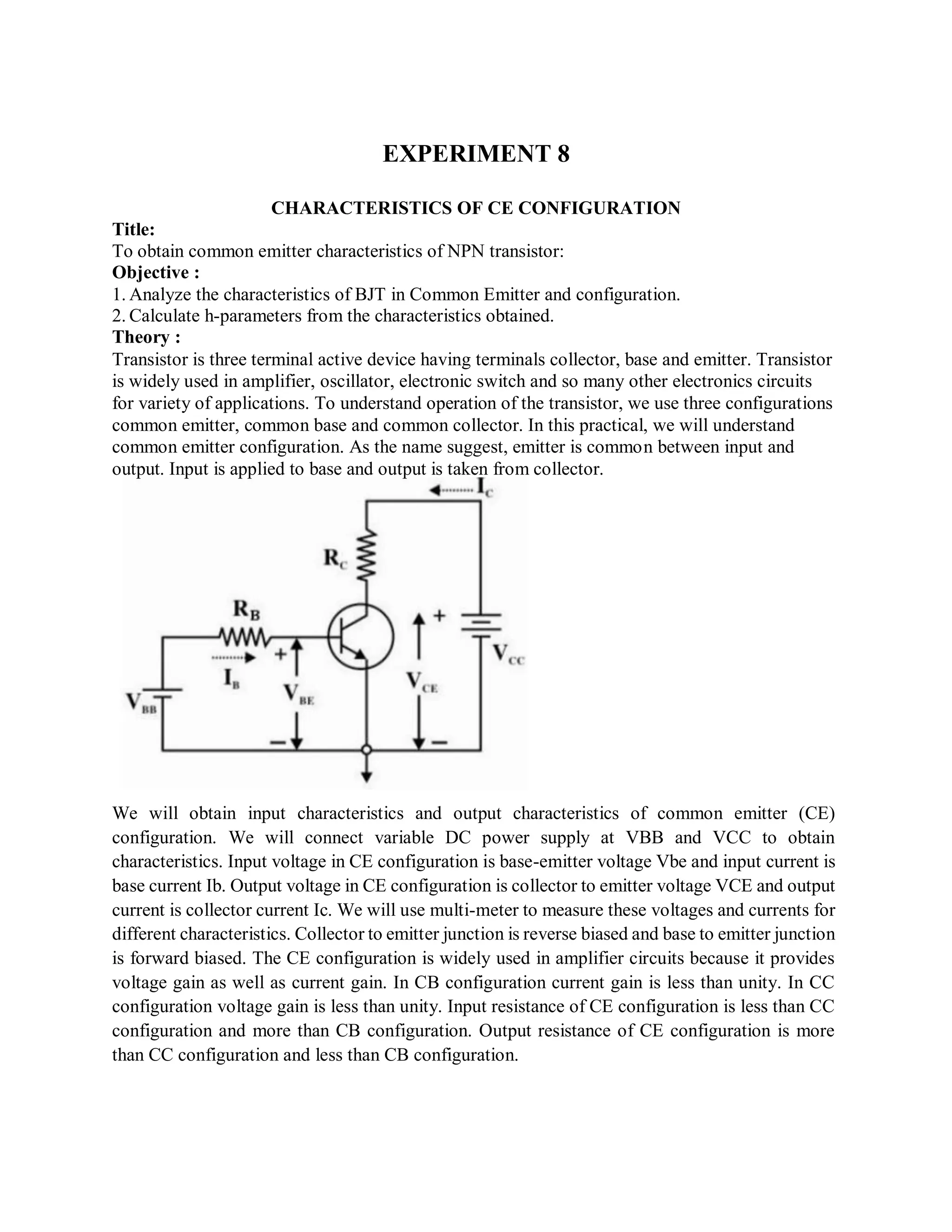
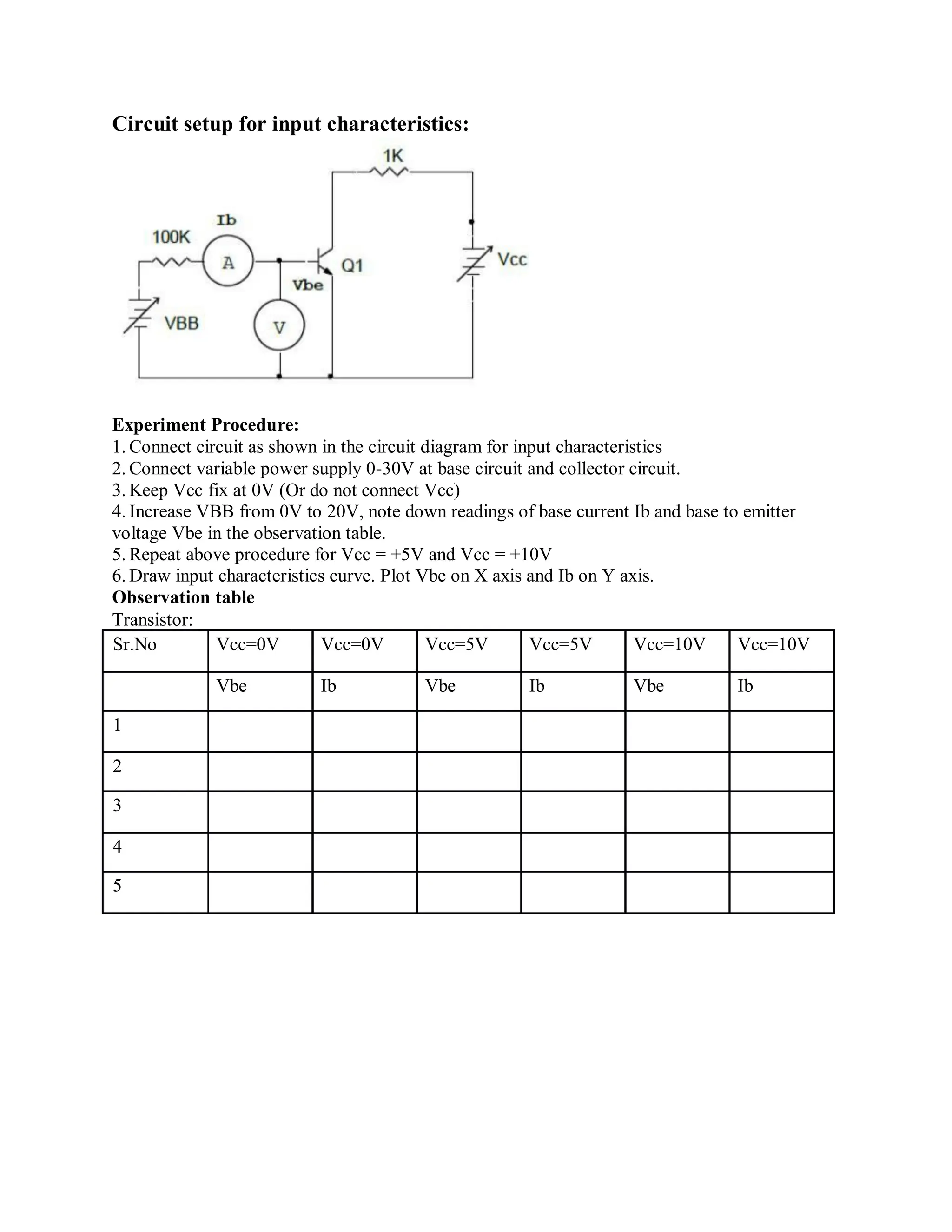
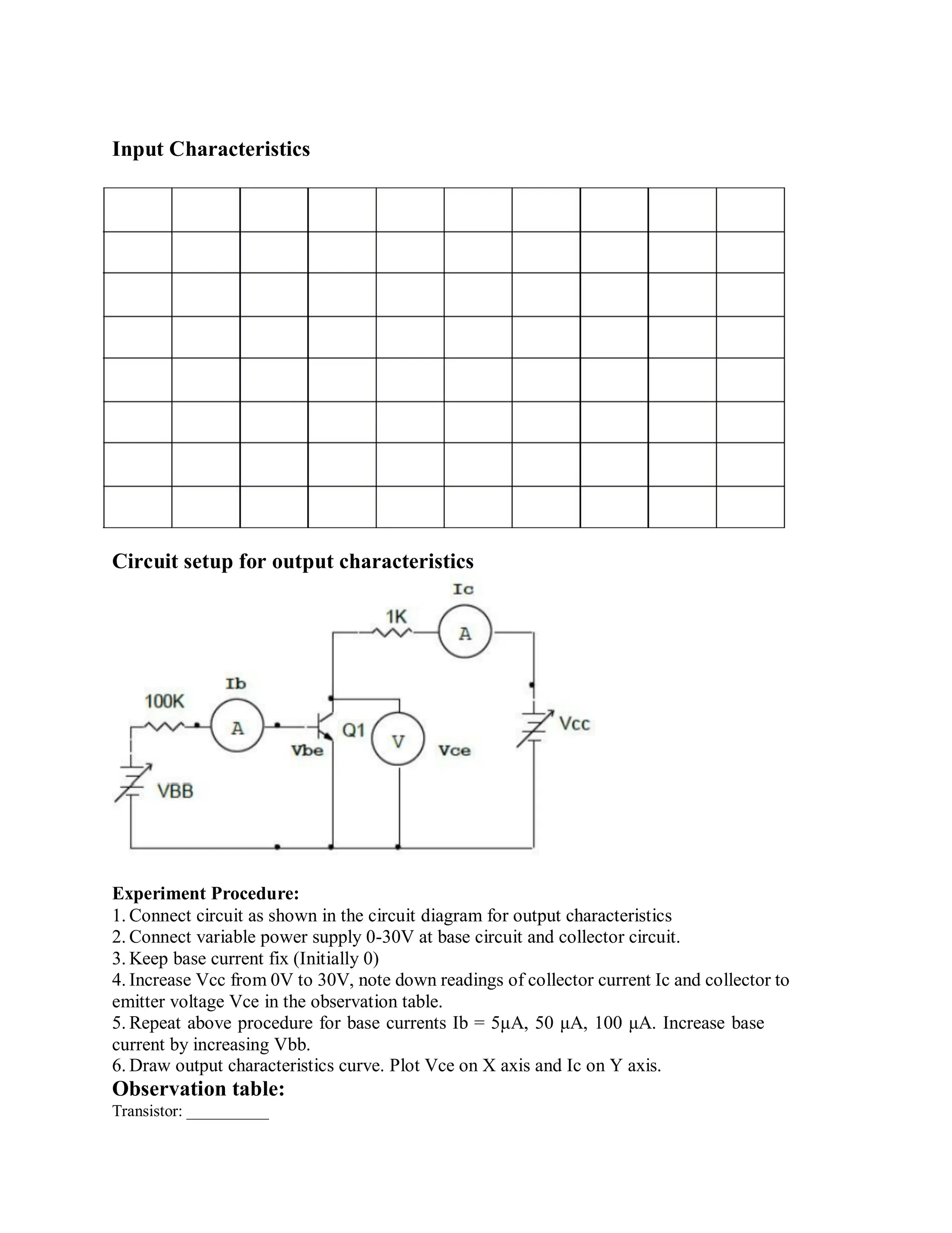
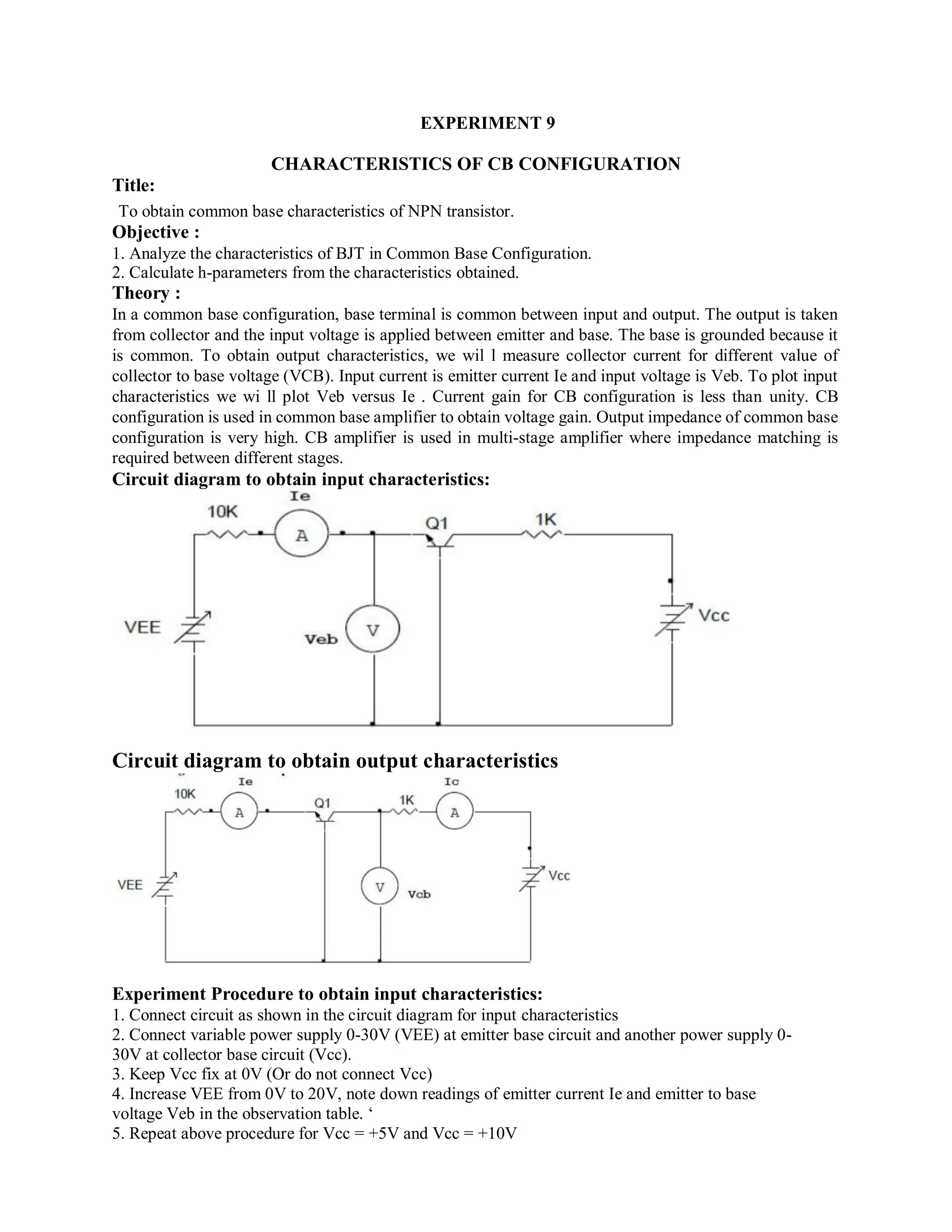
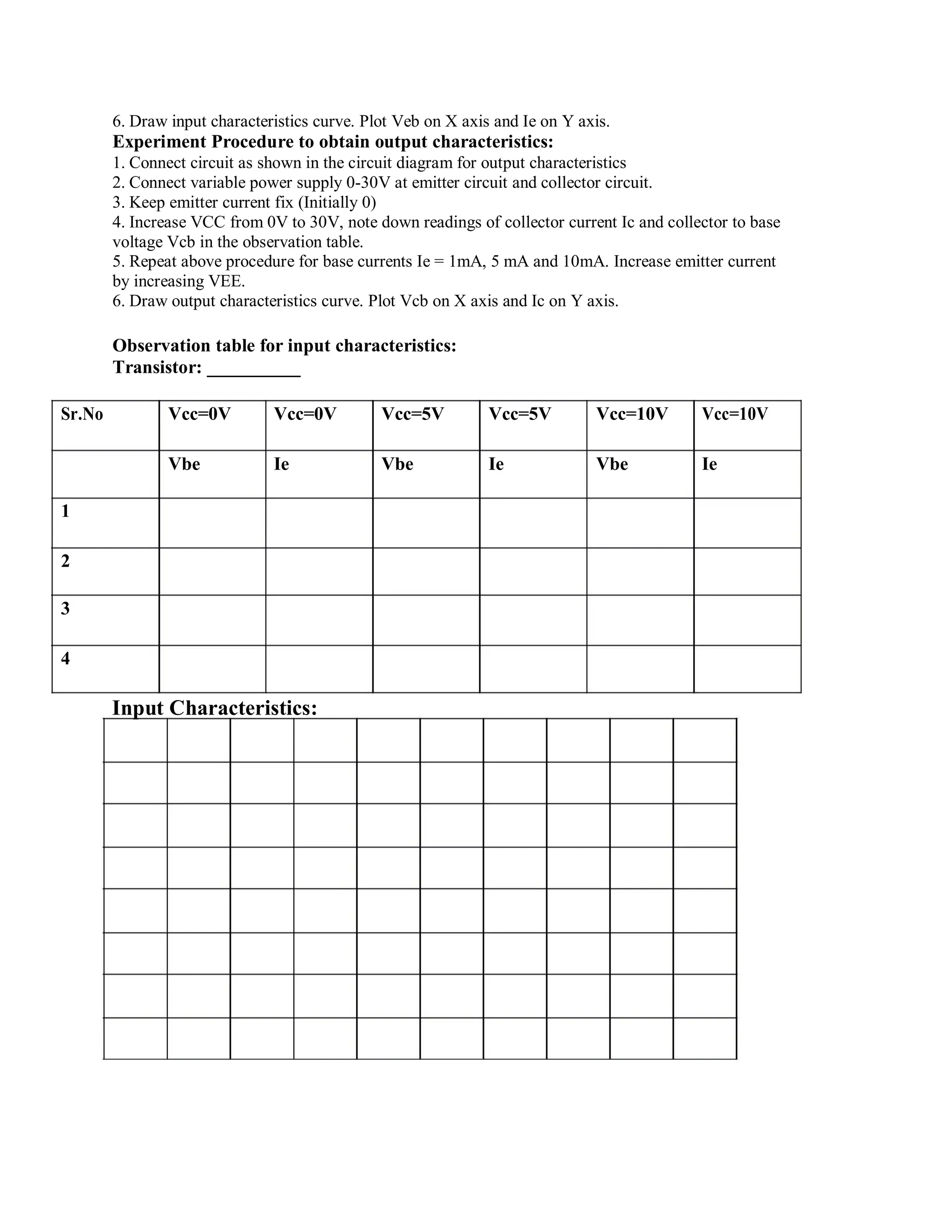
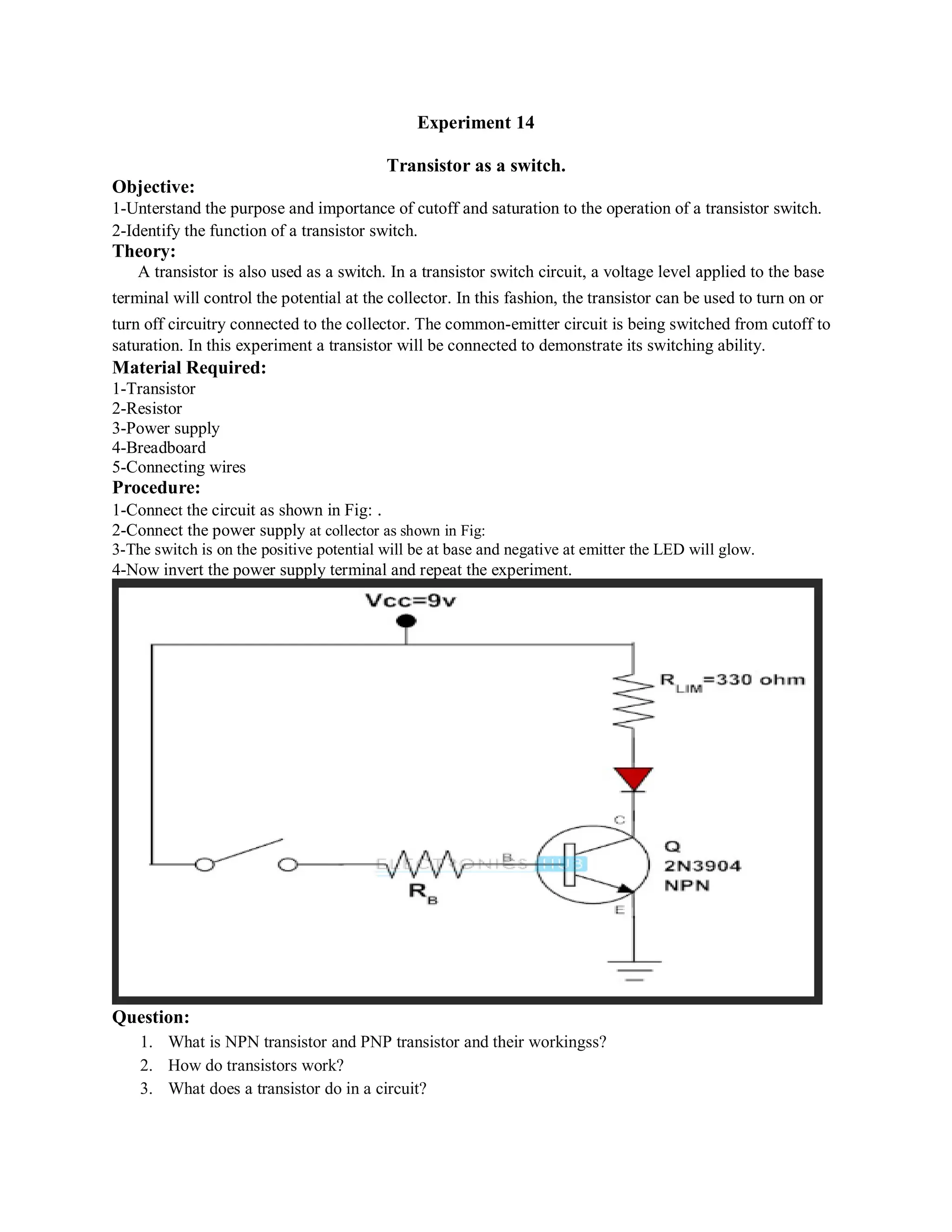
FRONT PAGE AND LIST OF EXPERIMENTS ARE MADE BUT PLACE IN
ANOTHER WORLD FILE THAT I SEND TO YOU DEAR WITH THIS MANAUL.
EXPERIMENT 1
DIODE CHARACTERISTICS
Objective
1. To identify the terminals of a diode correctly.
2. To determine experimentally the current and the voltage characteristics of a diode.
3. To understand the operation of a diode in dc circuit.
Theory
A diode is one of the electronic elements in a group of semiconductor devices with one junction.
Its structure consists of semiconductor materials which are silicon and germanium with p-type
and n-type combined together by the production process and filled into various types of tubes. A
diode has 2 terminals which are an anode (A) and cathode (K) as shown in Fig. 1-1.
(a) Appearance for a diode (b) Symbol for a diode
The Characteristics of a diode when forward-biased and reverse-biased (as shown in Fig. 1-2) are
that a diode can conduct the current in one direction when only forward-biased is applied, where
it cannot conduct the current when reverse-biased is applied.
Fig. 1-2 showing the operation of a diode.
Materials Required
1 Multimeter 1 Unit
2 Dual beams oscilloscope 1 Unit
3 Experiment Kit CES-100 1 Unit
4 Module : CES-103 1 Set
4.1 Diode : IN4007
4.2 Resistor : 1kΩ, 47Ω
5 Line cords 1 Set
Procedure:
Testing terminals of a diode
1.1 To identify the terminal property of a diode using in the experiment.
1.2 Use a multimeter to measure the resistance of a diode at the range of R x 10kΩ
Record the results in Table 1-1.
Table 1-1
Red wire Probe Black wire Probe Resistance (Ω)
A B
B A
1.3 From the measurement results of the resistance, terminal A is ……………
B is …………...
Characteristics of silicon diode
2.1 Connect the experimental circuit of Fig. 1-3
Fig. 1-3
the
2.2 Adjust the voltage Vin to the values which is listed in Table 1-2, then measure
values of VD, ID, Record the measured results in Table 1-2.
Table 1-2
Vin (Volts ) 0 0.2 0.4 0.6 0.8 1 2 3 4 5
VD (Volts)
ID (mA)
2.3 Reconnect the circuit by reversing the terminals of a diode to be reverse-biased.
2.4 Again adjust the voltage Vin to the indicated in Table 1-3 and measure the values of VD
and ID Record the measured results in Table 1-3.
Table 1-3
Vin (Volts ) 1 2 3 4 5 6 7 8 9 10
VD (Volts)
ID (mA)
2.5 From the data in Table 1-2 and Table 1-3, draw the relation graph of VD = f (ID)
of a silicon diode no. IN4007.
Graph 1-1
3. Determining the characteristics of germanium diode when forward– biased is
applied.
3.1 Connect the circuit as in step 2.1 so that the diode is forward-biased using the
germanium diode.
3.2 Adjust Vin to the values which is listed in Table 1-4 and measure VD, ID, Record the
results in Table 1-4
Table 1-4
Vin (Volts ) 0 0.2 0.4 0.6 0.8 1 2 3 4 5
VD (Volts)
ID (mA)
3.3 Reverse the diode terminals in step 3.1 and do the experiment again. Record the
results in Table 1-5.
Table 1-5
Vin (Volts ) 1 2 3 4 5 6 7 8 9 10
VD (Volts)
ID (mA)
3.4 Use the data in Table 1-4 and Table 1-5 to draw a graph showing the relation of VD
= f (ID) of Germanium diode.
Questions:
1. What is a semiconductor diode?
2. What are the properties of a diode?
3. When a diode is forward biased?
4. What are the uses of diode?
EXPERIMENT 2
HALF WAVE RECTIFIER CIRCUITS
Objective
1. To measure experimentally the input and the output waveforms.
2. To understand the operation of a filter circuit using the capacitor.
3. To select properly the filter circuit for the work.
Theory
Rectifier circuits are the circuits that use diodes to transform alternating current to direct
current. The basic rectifier circuit that is easy to use in the work is a-half wave rectifier
circuit as shown in Fig. 4-1 (a). The weak point of this circuit is that the ripple voltage at the
output of the circuit is too high. Then we have to use a large capacitor to filter voltage to be
level. The waveform characteristics are shown in Fig. 4-1 (b).
To connect a filter circuit using a capacitor to reduce the ripple voltage at the output
waveform of the circuit.
Materials Required
1. Oscilloscope 1 Unit
2. Experiment Kit CES-100 1 Unit
3. Module : CES-103
3.1 Resistor : 4.7 K Ω
3.2 Capacitors : 10 µF, 470 µF
3.3 Diode : IN4007 4 Line cords
Procedure:
1. Half wave rectifier Circuit.
2. 1.1 Connect the experimental circuit of Fig. 4-3
3. 1.2 Use an oscilloscope to measure the source voltage waveform (Vin), the
voltage drop across a diode (VD) and the voltage drop across load (Vout).
Record the voltage waveforms of Vin, VD and Vout using Graph 4-1
2. The results of the capacitor and the half – wave rectifier circuit.
2.1 Connect the experimental circuit of Fig. 4-4.
2.2 Using an oscilloscope, measure and record the voltage waveforms of Vin and
volt using Graph 4-2
2.3 In the circuit of Fig. 4-4, change the value of C form 10µF to 100µF. On the
oscilloscope screen, observe the changing Vout waveform and record in Graph
4-3
Questions:
• What is the principle of a rectifier?
• What are the applications of half wave rectifier?
• What are the advantages and disadvantages
of a half-wave rectifier?
EXPERIMENT 3
FULL WAVE RECTIFIER CIRCUITS WITH CENTER TAPED
Objective
1. To connect correctly a full wave rectifier circuit using with center taped.
2. To measure experimentally the voltage waveforms at the various parts of a circuit.
3. To understand the principle of using a capacitor to filter the voltage of a full wave
rectifier circuit with center taped.
Theory
A full wave rectifier circuit with center taped will use two rectifying diodes. Each diode will
rectify the alternating current (especially the positive) of the alternating voltage source to the
full wave direct voltage. This causes 2 waveforms in 1 alternating cycle of the source as
shown in Fig. 5-1. The quantity of the direct voltage at the output of the circuit will be 2
times more than a half wave rectifier circuit but the voltage PIV is 2 times of the maximum
voltage at the source Vin.
The capacitor known as the filter current will effect the circuit to generate more level
direct voltage and to have a lower ripple voltage than a half wave rectifier circuit.
Materials Required
1. Dual oscilloscope 1 Unit
2. Experiment Kit CES-100 1 Unit
3. Module : CES-103 1 Set
3.1 Resistor : 4.7 K Ω
3.2 Capacitor : 10 µF, 470 µF
3.3 Diode : IN4007 x 2 4 Line cords 1 Set
Procedure:
1. Full wave rectifier circuits with center taped.
1.1 Connect the circuit of Fig. 5-3
1.2 Use an oscilloscope to measure the voltage waveforms of VS1, VS2, VD1, VD2,
and Vout at the various parts of the circuit. Record the waveforms in Graph 5-1.
2. The filter circuit using a capacitor
2.1 Reconnect the experimental circuit by adding the 10 µF capacitor as in Fig. 5- 4.
2.2 Use an oscilloscope to measure the waveform of the voltage drop across load.
Draw the waveform in Graph 5-2.
2.3 In the circuit of Fig. 5-4 change the capacitor 10µF with 470µF. Again draw the
waveform of Vout in Graph 5-3.
Questions:
1. What is the frequency of AC component at the output of full wave rectifier? Give
reason.
2. What is the difference in DC output voltage in half wave and full wave rectifier for
the same AC input?
3. What is the efficiency of bridge rectifier?
4. Define Ripple factor „γ‟ and its values for the three types of rectifiers?
EXPERIMENT 4 & 5
CHARACTERISTICS AND APPLICATIONS OF A
ZENER DIODE
Objective
1. To determine experimentally the zener diode characteristics when forward – biased or
reverse – biased applied.
2. To understand the operation of zener diode in dc voltage regulator circuit.
3. To check and determine correctly the terminals of a zener diode.
Theory
A zener diode is one of the semiconductor devices which have 2 terminals as a diode. The
special characteristics of a zener diode which is different form the one of general diodes is
that when a zener diode is reverse – biased until it reaches the breakdown region, the voltage
drop across it is constant. That is the prominent of a zener diode which is applied to lots of
work. The symbol and the zener diode are shown in Fig. 2-1.
Zener diode are widely used to the work especially in dc voltage regulator circuits as shown
in Fig 2 -2 Generally, zener diodes product have the zener voltage limit form 2.4 volt to 200
volt.
Materials Required :
1 Multimeter 1 unit
2 Milliampmeter 1 Unit
3 Dual beam oscilloscope 1 Unit
4 Experiment Kit CES-100 1 Unit
5 Module : CES-103 1 Set
5.1 Zener diode 5.6V 1W
5.2 Resistors : 47Ω, 100 Ω, 1K Ω
5.3 Variable resistor : 2.2K Ω
6 Line cords 1 Set
Procedure:
1. Characteristics and applications of zener diode. 1.1 Determining the characteristics
of zener diode when forward biased is applied by connecting the circuit as Fig 2-3.
2. Adjust the voltage Vin to the values as shown in Table 2-1, Record the voltage VD
and current ID in Table 2-1.
3. Determining the Characteristics a zener diode when reverse-biased is applied by
connecting the circuit of Fig. 2-4 and reversing a diode in step 1-1.
4. Adjust the voltage Vin again to the values as listed in Table 2-2. Record the values of VD
and ID in Table 2-2.
5. Use the data Table 2-1 and Table 2-2 to draw a graph in graph 2-1. Showing the
relationship of VD = f (ID) of the 5.6V zener which is used in the experiment.
2. The use of a zener diode in a voltage regulator circuit:
2.1 Connect the circuit of Fig. 2-5, and then adjust the voltage Vin to 10 volt and RL to the
maximum value.
2.2 Reduce RL to the values as shown in Table 2-3. Measure the zener current (IZ), the
zener voltage (VZ), the load current (IL) and the current supplied form the source (IT).
Record the results in Table 2-3.
Questions:
What is Zener voltage?
Why is Zener diode used as a voltage regulator?
What is diode used for?
Can we use Zener diodes in a rectifier circuit
EXPERIMENT 6
CLIPPER CIRCUIT
Objective
1. To understand the use the diode switch to clip the various signal waveforms.
2. To measure correctly the various signal waveforms.
3. To calculate the experimental results comparing with the values in theory.
Theory
Diode Series Clipper Circuits:-
Series clipper circuits are the circuits which connect the diode series to the input signals.
(A diode is the electronic switch to clip the waveform). These circuits are divided into
2 types according to the ways of connection.
Negative series clipper circuits are the circuits which clip off the negative input
waveforms by connecting an anode of the diode D1 to the input which its voltage is +E.
The positive and negative output voltages are +(E-VF) and –(IS x R1) respectively IS is
the value of the leakage current when the diode obtains the reverse bias as shown in
Fig. 3-1(a).
Positive series clipper circuits, shown in Fig. 3-1 (b), are the circuits which connect the
diode series to the input signal by the cathode. When the input signal is set to be sine
signal at +E, the output waveforms dropping across R1 are read +(IS × R1) for the
positive signal and -(E-VF) for the negative signal.
(a) Negative series clipper
Materials Required
1. Multimeter 1 Unit
2. Dual oscilloscope 1 Unit
3. Experiment Kit CES-100 1 Unit
4. Module CES-107 1 Set
4.1 Resistors : 20KΩ
4.2 Capacitor : 1N4148
5. Line cord 1 Set
Procedure:
The Diode Series Clipper Circuits. 1.1
Connect the circuit of Fig. 3-4.
Fig. 3-4 The negative clipper circuit.
1.2 Set the oscilloscope as follows : channel 1 for input and channel 2 for output.
1.3 Using the oscilloscope, measure the input voltage (Vin) and the output voltage
(Vout). Draw the measured output waveform in Graphs 3-1(b).
1.4 Reconnect the circuit of Fig 3-4 by inverting the diode terminal as illustrated
in Fig. 3-5.
Fig. 3-5 The positive clipper circuit.
1.5 Repeat steps 1.2, 1.3 and record the output voltage diagram in Graph 3-1 (c).
Questions:
1. What is Positive clipping?
2. What is Negative clipping of circuit?
3. What are different types of clipping?
EXPERIMENT 7
CLAMPER CIRCUITS
Objective
1. To study the operations of the clamper circuits using diodes and capacitors.
2. To experimentally measure the input and output waveforms of the circuits.
3. To calculate the appropriate resistance in order to set correctly the operation of
the clamper circuit.
4. To experimentally measure the voltage drop across the various parts of the circuit.
Theory
The Clamper Circuit:-
The circuit that adjusts the level of the input voltage waveform to the negative by remaining
the amplitude of the signal is called the negative voltage clamper as shown in Fig. 4-1 (a).
The components of the circuit are the capacitor. (C1), the diode (D1) and the resistor (R1).
(a) The negative voltage clamper circuit
(b) The positive voltage clamper circuit.
Fig. 4-1 Negative and positive voltage clamper circuit.
1.
Apparatus:-
Multimeter 1 Unit
2. Dual oscilloscope 1 Unit
3. Experiment Kit CES-100 1 Unit
4. Module CES-107 1 Set
4.1 Diode : 1N4148
4.2 Resistors : 20K Ω
4.3 Capacitor : 2.2µF
5. Line cord 1 Set
Procedure:
Positive Clamper Circuits 1.1
Connect the circuit of Fig. 4-4
Fig. 4-4 The positive clamper circuit
1.2 Using an oscilloscope, use channel 1 and 2 to measure the input voltage
waveform and the output voltage waveform record the measured waveforms
in graphs 4-1 (b).
1.3 Use the multimeter to measure Vc, Vc = ……………………………. Volts.
1.4 Reconnect the circuit by using the 1.5V battery to bias with the diode as Fig.
4-5 (Bias Positive Clamper).
1.5 Repeat step 1.2, measure and draw the output voltage waveform again in graph
4-1(c).
1.6 Use the multimeter to measure Vc, Vc = …………………………….Volts.
Graph 4-1
Negative Clamper Circuits 2.1
Connect the circuit of Fig. 4-6.
Fig. 4-6 The negative clamper circuit.
2.2 Repeat step 1.2 in procedures 1.
2.3 With an oscilloscope, use channel 1 and 2 to measure the input
voltage and the output voltage waveform record in Graph 4-2 (b).
2.4 Use the multimeter to measure Vc, Vc = …………………….volts.
2.5 Reconnect the circuit by using the 1.5 V battery to bias with the
diode as in Fig. 4-7.
Fig 4-7 The bias negative clamper circuit.
2.6 Again use the oscilloscope to measure the output voltage waveform. Record
the results in Graph 4-2 (c).
2.7 Use the multimeter to measure Vc, Vc = ………………………….. volts.
Questions:
1. What is Positive clamping?
2. What is Negative clamping?
3. What are different types of clamping?
EXPERIMENT 8
CHARACTERISTICS OF CE CONFIGURATION
Title:
To obtain common emitter characteristics of NPN transistor:
Objective :
1. Analyze the characteristics of BJT in Common Emitter and configuration.
2. Calculate h-parameters from the characteristics obtained.
Theory :
Transistor is three terminal active device having terminals collector, base and emitter. Transistor
is widely used in amplifier, oscillator, electronic switch and so many other electronics circuits
for variety of applications. To understand operation of the transistor, we use three configurations
common emitter, common base and common collector. In this practical, we will understand
common emitter configuration. As the name suggest, emitter is common between input and
output. Input is applied to base and output is taken from collector.
We will obtain input characteristics and output characteristics of common emitter (CE)
configuration. We will connect variable DC power supply at VBB and VCC to obtain
characteristics. Input voltage in CE configuration is base-emitter voltage Vbe and input current is
base current Ib. Output voltage in CE configuration is collector to emitter voltage VCE and output
current is collector current Ic. We will use multi-meter to measure these voltages and currents for
different characteristics. Collector to emitter junction is reverse biased and base to emitter junction
is forward biased. The CE configuration is widely used in amplifier circuits because it provides
voltage gain as well as current gain. In CB configuration current gain is less than unity. In CC
configuration voltage gain is less than unity. Input resistance of CE configuration is less than CC
configuration and more than CB configuration. Output resistance of CE configuration is more
than CC configuration and less than CB configuration.
Circuit setup for input characteristics:
Experiment Procedure:
1. Connect circuit as shown in the circuit diagram for input characteristics
2. Connect variable power supply 0-30V at base circuit and collector circuit.
3. Keep Vcc fix at 0V (Or do not connect Vcc)
4. Increase VBB from 0V to 20V, note down readings of base current Ib and base to emitter
voltage Vbe in the observation table.
5. Repeat above procedure for Vcc = +5V and Vcc = +10V
6. Draw input characteristics curve. Plot Vbe on X axis and Ib on Y axis.
Observation table
Transistor: __________
Sr.No Vcc=0V Vcc=0V Vcc=5V Vcc=5V Vcc=10V Vcc=10V
Vbe Ib Vbe Ib Vbe Ib
1
2
3
4
5
Input Characteristics
Circuit setup for output characteristics
Experiment Procedure:
1. Connect circuit as shown in the circuit diagram for output characteristics
2. Connect variable power supply 0-30V at base circuit and collector circuit.
3. Keep base current fix (Initially 0)
4. Increase Vcc from 0V to 30V, note down readings of collector current Ic and collector to
emitter voltage Vce in the observation table.
5. Repeat above procedure for base currents Ib = 5μA, 50 μA, 100 μA. Increase base
current by increasing Vbb.
6. Draw output characteristics curve. Plot Vce on X axis and Ic on Y axis.
Observation table:
Transistor: __________
Sr.No Ib=0 Ib=0 Ib=5 Ib=5 Ib=50 Ib=50 Ib=100 Ib=100
Vce Ic Vce Ic Vce Ic Vce Ic
1
2
3
4
5
6
Output Characteristics
Questions:
1. How to check type of transistor (NPN or PNP) with help of multimeter?
2. Define current gain of the transistor in CE configuration. What is the DC current gain you obtain
in this practical?
3. To operate a transistor as amplifier, emitter junction is forward biased and collector junction is
reverse biased. Why?
4. For amplification CE is preferred, why?
EXPERIMENT 9
CHARACTERISTICS OF CB CONFIGURATION
Title:
To obtain common base characteristics of NPN transistor.
Objective :
1. Analyze the characteristics of BJT in Common Base Configuration.
2. Calculate h-parameters from the characteristics obtained.
Theory :
In a common base configuration, base terminal is common between input and output. The output is taken
from collector and the input voltage is applied between emitter and base. The base is grounded because it
is common. To obtain output characteristics, we wil l measure collector current for different value of
collector to base voltage (VCB). Input current is emitter current Ie and input voltage is Veb. To plot input
characteristics we wi ll plot Veb versus Ie . Current gain for CB configuration is less than unity. CB
configuration is used in common base amplifier to obtain voltage gain. Output impedance of common base
configuration is very high. CB amplifier is used in multi-stage amplifier where impedance matching is
required between different stages.
Circuit diagram to obtain input characteristics:
Circuit diagram to obtain output characteristics
Experiment Procedure to obtain input characteristics:
1. Connect circuit as shown in the circuit diagram for input characteristics
2. Connect variable power supply 0-30V (VEE) at emitter base circuit and another power supply 0-
30V at collector base circuit (Vcc).
3. Keep Vcc fix at 0V (Or do not connect Vcc)
4. Increase VEE from 0V to 20V, note down readings of emitter current Ie and emitter to base
voltage Veb in the observation table. ‘
5. Repeat above procedure for Vcc = +5V and Vcc = +10V
6. Draw input characteristics curve. Plot Veb on X axis and Ie on Y axis.
Experiment Procedure to obtain output characteristics:
1. Connect circuit as shown in the circuit diagram for output characteristics
2. Connect variable power supply 0-30V at emitter circuit and collector circuit.
3. Keep emitter current fix (Initially 0)
4. Increase VCC from 0V to 30V, note down readings of collector current Ic and collector to base
voltage Vcb in the observation table.
5. Repeat above procedure for base currents Ie = 1mA, 5 mA and 10mA. Increase emitter current
by increasing VEE.
6. Draw output characteristics curve. Plot Vcb on X axis and Ic on Y axis.
Observation table for input characteristics:
Transistor: __________
Sr.No Vcc=0V Vcc=0V Vcc=5V Vcc=5V Vcc=10V Vcc=10V
Vbe Ie Vbe Ie Vbe Ie
1
2
3
4
Input Characteristics:
Observation table for output characteristics:
Sr.No Ie=0 A Ie=0 A Ie=1m A Ie=1m A Ie=5m A Ie=5m A Ie=10m A Ie=1
Vce Ic Vce Ic Vce Ic Vce Ic
1
2
3
4
5
6
7
Transistor: __________
Output Characteristics:
Questions:
1. What are the applications of CB configuration?
2. What are the input and output impedances of CB configuration?
3. What is EARLY effect?
4. Draw diagram of CB configuration for PNP transistor?
5. What is the power gain of CB configuration?
EXPERIMENT 10
Characteristics of Common Collector Configuration:
Objective:
To obtain common collector configuration of power NPN transistor.
Theory:
In common collector configuration, collector is common between input and output
terminal. The collector is grounded because it is commom. The output is taken from base and
input is applied between emitter and collector.
Apparatus required:
Breadboard
Connecting wires
Transistor
Multimeter
Power supply
Resistors (1kὩ)
Circuit diagram:
Procedure:
For input characteristics:
1. Draw and Connect the circuit itself logically as above..
2. Connect variable power supply 0-30volts at the collector and base circuit.
3. Keep VCC fix at 0 volt.
4. Increase VEE from 0 -2o volt and note down the readings for Ib and Vbc.
5. Repeat above procedure for VEE at 5Vand 10V.
6. Plot the graph between Ib and Vbe.
Table for input characterstics:
SR NO. VEE VCC =0V VCC=0V VCC =5V VCC =5V VCC =10V VCC
Graph:
Procedure:
For output characteristics:
1. Connect the circuit as shown in figure.
2. Connect the power supply at the base and emitter circuit.
3. Keep base current fix.
4. Increase VEE from 0 -20 volt and note down the readings for emitter current Ie and emitter
collector voltage Vec.
5. Repeat above procedure for increaing Ib and note down the readings
6. Plot the graph between Ie and Vec.
Table for output characteristics:
SR NO. VEE Ib = Ib = Ib = Ib = Ib = Ib =
mA mA mA mA mA mA
Vec (V) Ie (mA) Vec (V) Ie (mA) Vec (V) Ie (mA)
1
2
3
4
5
Graph:
Conclusion:
Questions:
1. What is an emitter follower?
2. What is a common emitter amplifier?
3. How to measure output impedance?
4. What is input resistance?
5. How to calculate impedance?
EXPERIMENT 11
Characteristics of Common Gate Configuration:
Objective:
To obtain common gate configuration of power MOSFET.
Theory:
In common gate configuration, gate is common between input and output terminal. The
gate is grounded because it is common. To obtain the output characteristics ,drain current will be
measured Voc (drain to gate). For obtaining input characteristics, IB current will be measured
across source by changing voltage across source.
Apparatus required:
i. Breadboard
ii. Power Supply
iii. MOSFET and resistors
iv. Connecting Wires
v. Multimeter
Circuit diagram:
Procedure:
For input characteristics:
7. Connect the circuit as shown in fig.a.
8. Connect variable power supply 0-30volts at the drain and power supply at the source terminals.
9. Keep VCC fox at 0 volt.
10. Increase VGS from 0 -30 volt and note down the readings for current across source IS.
11. Repeat above procedure for VDD =5V.
12. Plot the graph between IS and VGS.
Table for input characteristics:
Sr .no VDD =0V. VDD =0V. VDD =5V. VDD =5V.
VGS (V) IS (mA) VGS (V) IS (mA)
1
2
3
4
5
Graph:
Procedure:
For output characteristics:
7. Connect the circuit as shown in fig.
8. Connect the power supply as connected above in the input.
9. Keep IS and VSS fix.
10. Increase VGD from 0 -30 volt and note down the readings for current across source ID.
11. Repeat above procedure for VSS =5V.
12. Plot the graph between ID and VGD.
Table for output characteristics:
Sr. no IS =0A IS =0A IS =1.2mA IS = 1.2Ma
VGD (V) ID (mA) VGD (V) ID (mA)
1
2
3
4
5
Graph:
Question:
1. What is amplifier?
2. Which configuration has maximum gain?
3. What is impedances of the common gate?
EXPERIMENT # 12
Characteristics of Common source Configuration
Objective:
To obtain common source configuration of power MOSFET.
Theory:
In common source configuration, source is common between input and output terminal. The
source is grounded because it is common. The input characteristics does not operate because Dc current ,
no current flows through gate. The output will be obtained by changing the voltage across Vos and
measure the drain current .
Apparatus required:
i. Breadboard
ii. Power Supply
iii. MOSFET and resistors
iv. Connecting Wires
v. Multimeter
Circuit diagram:
Procedure :
For output characteristics:
Connect the circuit as shown in fig.b.
Connect the variable power supply o-30 v as connected above in the
input. Keep the VGG constant ( fix).
Increase VDS from 0 -30 volt and note down the readings of drain current
. Repeat above procedure for VGG =10V.
Plot the graph between VDS and ID to obtain the output characteristics.
Graph:-
Table for output characteristics:
Sr.no VGG = 5V VGG = 5V VG = 10V VG =10V
VGS (V) ID (mA) VGD (V) ID(mA)
1
2
3
4
5
6
Questions:
1. What are the advantage and disadvantage in common source?
2. What is MOSFET voltage gain in common source?
EXPERIMENT # 13
Characteristics of Common Drain Configuration:
Objective:
To obtain common Drain configuration of power MOSFET.
Theory:
In common Drain configuration, Drain is common between input and output terminal. The Drain
is grounded because it is common. The input Characteristics obtained as we applying direct current. The
output will be obtained by change in VSD and measuring IS .
Apparatus required:
i. Breadboard
ii. Multimeter
iii. MOSFET and Resistors
iv. Connecting Wires
Circuit diagram:
Procedure:
For output characteristics:
Connect the circuit as shown in fig.b.
Connect the power supply as connected above in the
input. Keep the VGG fix VGG = 0V .
Increase VGD from 0 -30 volt and note down the readings of source current IS .
Repeat above procedure for VGG =5V.
Plot the graph between VSD and IS to obtained output characteristics .
Table for output characteristics:
Sr .no VGG = 5V VGG = 5V VGG = 5V VGG = 5V
VSD (V) IS (mA) VSD (V) IS (mA)
1
2
3
4
5
Graph:
Conclusion:
Question:
1. What are the advantage and disadvantage in common source?
2. What is MOSFET voltage gain in common source?
Experiment 14
Transistor as a switch.
Objective:
1-Unterstand the purpose and importance of cutoff and saturation to the operation of a transistor switch.
2-Identify the function of a transistor switch.
Theory:
A transistor is also used as a switch. In a transistor switch circuit, a voltage level applied to the base
terminal will control the potential at the collector. In this fashion, the transistor can be used to turn on or
turn off circuitry connected to the collector. The common-emitter circuit is being switched from cutoff to
saturation. In this experiment a transistor will be connected to demonstrate its switching ability.
Material Required:
1-Transistor
2-Resistor
3-Power supply
4-Breadboard
5-Connecting wires
Procedure:
1-Connect the circuit as shown in Fig: .
2-Connect the power supply at collector as shown in Fig:
3-The switch is on the positive potential will be at base and negative at emitter the LED will glow.
4-Now invert the power supply terminal and repeat the experiment.
Question:
1. What is NPN transistor and PNP transistor and their workingss?
2. How do transistors work?
3. What does a transistor do in a circuit?
Experiment 15
MOSFET as a switch.
Objective:
To learn how MOSFET is used as a switch and its working.
Theory:
MOSFET are very good electric switches for controlling loads and in CMOS digital circuits as
they operate between their cutoff and saturation region.
Material required:
1-MOSFET
2-Resistor
3-LED
4-Power supply
5-Connecting wire
6-Breadboard
Procedure:
1-Connect the circuit as shown in fig.
2-Connect the power supply to apply DC.
3- Turn on the switch the positive potential at gate and negative is at source. The LED will glow.
4-Now reverse the power supply terminals and repeat experiment.
Questions:
What is a power MOSFET?
How does a MOSFET work?
How does a N-channel MOSFET work?
How does a P channel MOSFET work?

EDC.pdf

  • 1.
    FRONT PAGE ANDLIST OF EXPERIMENTS ARE MADE BUT PLACE IN ANOTHER WORLD FILE THAT I SEND TO YOU DEAR WITH THIS MANAUL.
  • 2.
    EXPERIMENT 1 DIODE CHARACTERISTICS Objective 1.To identify the terminals of a diode correctly. 2. To determine experimentally the current and the voltage characteristics of a diode. 3. To understand the operation of a diode in dc circuit. Theory A diode is one of the electronic elements in a group of semiconductor devices with one junction. Its structure consists of semiconductor materials which are silicon and germanium with p-type and n-type combined together by the production process and filled into various types of tubes. A diode has 2 terminals which are an anode (A) and cathode (K) as shown in Fig. 1-1. (a) Appearance for a diode (b) Symbol for a diode The Characteristics of a diode when forward-biased and reverse-biased (as shown in Fig. 1-2) are that a diode can conduct the current in one direction when only forward-biased is applied, where it cannot conduct the current when reverse-biased is applied. Fig. 1-2 showing the operation of a diode.
  • 3.
    Materials Required 1 Multimeter1 Unit 2 Dual beams oscilloscope 1 Unit 3 Experiment Kit CES-100 1 Unit 4 Module : CES-103 1 Set 4.1 Diode : IN4007 4.2 Resistor : 1kΩ, 47Ω 5 Line cords 1 Set Procedure: Testing terminals of a diode 1.1 To identify the terminal property of a diode using in the experiment. 1.2 Use a multimeter to measure the resistance of a diode at the range of R x 10kΩ Record the results in Table 1-1. Table 1-1 Red wire Probe Black wire Probe Resistance (Ω) A B B A 1.3 From the measurement results of the resistance, terminal A is …………… B is …………... Characteristics of silicon diode 2.1 Connect the experimental circuit of Fig. 1-3 Fig. 1-3 the 2.2 Adjust the voltage Vin to the values which is listed in Table 1-2, then measure values of VD, ID, Record the measured results in Table 1-2.
  • 4.
    Table 1-2 Vin (Volts) 0 0.2 0.4 0.6 0.8 1 2 3 4 5 VD (Volts) ID (mA) 2.3 Reconnect the circuit by reversing the terminals of a diode to be reverse-biased. 2.4 Again adjust the voltage Vin to the indicated in Table 1-3 and measure the values of VD and ID Record the measured results in Table 1-3. Table 1-3 Vin (Volts ) 1 2 3 4 5 6 7 8 9 10 VD (Volts) ID (mA) 2.5 From the data in Table 1-2 and Table 1-3, draw the relation graph of VD = f (ID) of a silicon diode no. IN4007. Graph 1-1 3. Determining the characteristics of germanium diode when forward– biased is applied. 3.1 Connect the circuit as in step 2.1 so that the diode is forward-biased using the germanium diode. 3.2 Adjust Vin to the values which is listed in Table 1-4 and measure VD, ID, Record the results in Table 1-4
  • 5.
    Table 1-4 Vin (Volts) 0 0.2 0.4 0.6 0.8 1 2 3 4 5 VD (Volts) ID (mA) 3.3 Reverse the diode terminals in step 3.1 and do the experiment again. Record the results in Table 1-5. Table 1-5 Vin (Volts ) 1 2 3 4 5 6 7 8 9 10 VD (Volts) ID (mA) 3.4 Use the data in Table 1-4 and Table 1-5 to draw a graph showing the relation of VD = f (ID) of Germanium diode. Questions: 1. What is a semiconductor diode? 2. What are the properties of a diode? 3. When a diode is forward biased? 4. What are the uses of diode?
  • 7.
    EXPERIMENT 2 HALF WAVERECTIFIER CIRCUITS Objective 1. To measure experimentally the input and the output waveforms. 2. To understand the operation of a filter circuit using the capacitor. 3. To select properly the filter circuit for the work. Theory Rectifier circuits are the circuits that use diodes to transform alternating current to direct current. The basic rectifier circuit that is easy to use in the work is a-half wave rectifier circuit as shown in Fig. 4-1 (a). The weak point of this circuit is that the ripple voltage at the output of the circuit is too high. Then we have to use a large capacitor to filter voltage to be level. The waveform characteristics are shown in Fig. 4-1 (b). To connect a filter circuit using a capacitor to reduce the ripple voltage at the output waveform of the circuit. Materials Required 1. Oscilloscope 1 Unit 2. Experiment Kit CES-100 1 Unit 3. Module : CES-103 3.1 Resistor : 4.7 K Ω 3.2 Capacitors : 10 µF, 470 µF 3.3 Diode : IN4007 4 Line cords
  • 8.
    Procedure: 1. Half waverectifier Circuit. 2. 1.1 Connect the experimental circuit of Fig. 4-3 3. 1.2 Use an oscilloscope to measure the source voltage waveform (Vin), the voltage drop across a diode (VD) and the voltage drop across load (Vout). Record the voltage waveforms of Vin, VD and Vout using Graph 4-1 2. The results of the capacitor and the half – wave rectifier circuit. 2.1 Connect the experimental circuit of Fig. 4-4.
  • 9.
    2.2 Using anoscilloscope, measure and record the voltage waveforms of Vin and volt using Graph 4-2 2.3 In the circuit of Fig. 4-4, change the value of C form 10µF to 100µF. On the oscilloscope screen, observe the changing Vout waveform and record in Graph 4-3 Questions: • What is the principle of a rectifier? • What are the applications of half wave rectifier? • What are the advantages and disadvantages of a half-wave rectifier?
  • 10.
    EXPERIMENT 3 FULL WAVERECTIFIER CIRCUITS WITH CENTER TAPED Objective 1. To connect correctly a full wave rectifier circuit using with center taped. 2. To measure experimentally the voltage waveforms at the various parts of a circuit. 3. To understand the principle of using a capacitor to filter the voltage of a full wave rectifier circuit with center taped. Theory A full wave rectifier circuit with center taped will use two rectifying diodes. Each diode will rectify the alternating current (especially the positive) of the alternating voltage source to the full wave direct voltage. This causes 2 waveforms in 1 alternating cycle of the source as shown in Fig. 5-1. The quantity of the direct voltage at the output of the circuit will be 2 times more than a half wave rectifier circuit but the voltage PIV is 2 times of the maximum voltage at the source Vin. The capacitor known as the filter current will effect the circuit to generate more level direct voltage and to have a lower ripple voltage than a half wave rectifier circuit.
  • 11.
    Materials Required 1. Dualoscilloscope 1 Unit 2. Experiment Kit CES-100 1 Unit 3. Module : CES-103 1 Set 3.1 Resistor : 4.7 K Ω 3.2 Capacitor : 10 µF, 470 µF 3.3 Diode : IN4007 x 2 4 Line cords 1 Set Procedure: 1. Full wave rectifier circuits with center taped. 1.1 Connect the circuit of Fig. 5-3 1.2 Use an oscilloscope to measure the voltage waveforms of VS1, VS2, VD1, VD2, and Vout at the various parts of the circuit. Record the waveforms in Graph 5-1.
  • 12.
    2. The filtercircuit using a capacitor 2.1 Reconnect the experimental circuit by adding the 10 µF capacitor as in Fig. 5- 4. 2.2 Use an oscilloscope to measure the waveform of the voltage drop across load. Draw the waveform in Graph 5-2.
  • 13.
    2.3 In thecircuit of Fig. 5-4 change the capacitor 10µF with 470µF. Again draw the waveform of Vout in Graph 5-3. Questions: 1. What is the frequency of AC component at the output of full wave rectifier? Give reason. 2. What is the difference in DC output voltage in half wave and full wave rectifier for the same AC input? 3. What is the efficiency of bridge rectifier? 4. Define Ripple factor „γ‟ and its values for the three types of rectifiers?
  • 14.
    EXPERIMENT 4 &5 CHARACTERISTICS AND APPLICATIONS OF A ZENER DIODE Objective 1. To determine experimentally the zener diode characteristics when forward – biased or reverse – biased applied. 2. To understand the operation of zener diode in dc voltage regulator circuit. 3. To check and determine correctly the terminals of a zener diode. Theory A zener diode is one of the semiconductor devices which have 2 terminals as a diode. The special characteristics of a zener diode which is different form the one of general diodes is that when a zener diode is reverse – biased until it reaches the breakdown region, the voltage drop across it is constant. That is the prominent of a zener diode which is applied to lots of work. The symbol and the zener diode are shown in Fig. 2-1. Zener diode are widely used to the work especially in dc voltage regulator circuits as shown in Fig 2 -2 Generally, zener diodes product have the zener voltage limit form 2.4 volt to 200 volt.
  • 15.
    Materials Required : 1Multimeter 1 unit 2 Milliampmeter 1 Unit 3 Dual beam oscilloscope 1 Unit 4 Experiment Kit CES-100 1 Unit 5 Module : CES-103 1 Set 5.1 Zener diode 5.6V 1W 5.2 Resistors : 47Ω, 100 Ω, 1K Ω 5.3 Variable resistor : 2.2K Ω 6 Line cords 1 Set Procedure: 1. Characteristics and applications of zener diode. 1.1 Determining the characteristics of zener diode when forward biased is applied by connecting the circuit as Fig 2-3. 2. Adjust the voltage Vin to the values as shown in Table 2-1, Record the voltage VD and current ID in Table 2-1.
  • 16.
    3. Determining theCharacteristics a zener diode when reverse-biased is applied by connecting the circuit of Fig. 2-4 and reversing a diode in step 1-1. 4. Adjust the voltage Vin again to the values as listed in Table 2-2. Record the values of VD and ID in Table 2-2. 5. Use the data Table 2-1 and Table 2-2 to draw a graph in graph 2-1. Showing the relationship of VD = f (ID) of the 5.6V zener which is used in the experiment. 2. The use of a zener diode in a voltage regulator circuit: 2.1 Connect the circuit of Fig. 2-5, and then adjust the voltage Vin to 10 volt and RL to the maximum value.
  • 17.
    2.2 Reduce RLto the values as shown in Table 2-3. Measure the zener current (IZ), the zener voltage (VZ), the load current (IL) and the current supplied form the source (IT). Record the results in Table 2-3.
  • 18.
    Questions: What is Zenervoltage? Why is Zener diode used as a voltage regulator? What is diode used for? Can we use Zener diodes in a rectifier circuit
  • 19.
    EXPERIMENT 6 CLIPPER CIRCUIT Objective 1.To understand the use the diode switch to clip the various signal waveforms. 2. To measure correctly the various signal waveforms. 3. To calculate the experimental results comparing with the values in theory. Theory Diode Series Clipper Circuits:- Series clipper circuits are the circuits which connect the diode series to the input signals. (A diode is the electronic switch to clip the waveform). These circuits are divided into 2 types according to the ways of connection. Negative series clipper circuits are the circuits which clip off the negative input waveforms by connecting an anode of the diode D1 to the input which its voltage is +E. The positive and negative output voltages are +(E-VF) and –(IS x R1) respectively IS is the value of the leakage current when the diode obtains the reverse bias as shown in Fig. 3-1(a). Positive series clipper circuits, shown in Fig. 3-1 (b), are the circuits which connect the diode series to the input signal by the cathode. When the input signal is set to be sine signal at +E, the output waveforms dropping across R1 are read +(IS × R1) for the positive signal and -(E-VF) for the negative signal. (a) Negative series clipper
  • 21.
    Materials Required 1. Multimeter1 Unit 2. Dual oscilloscope 1 Unit 3. Experiment Kit CES-100 1 Unit 4. Module CES-107 1 Set 4.1 Resistors : 20KΩ 4.2 Capacitor : 1N4148 5. Line cord 1 Set Procedure: The Diode Series Clipper Circuits. 1.1 Connect the circuit of Fig. 3-4. Fig. 3-4 The negative clipper circuit. 1.2 Set the oscilloscope as follows : channel 1 for input and channel 2 for output. 1.3 Using the oscilloscope, measure the input voltage (Vin) and the output voltage (Vout). Draw the measured output waveform in Graphs 3-1(b). 1.4 Reconnect the circuit of Fig 3-4 by inverting the diode terminal as illustrated in Fig. 3-5. Fig. 3-5 The positive clipper circuit.
  • 22.
    1.5 Repeat steps1.2, 1.3 and record the output voltage diagram in Graph 3-1 (c). Questions: 1. What is Positive clipping? 2. What is Negative clipping of circuit? 3. What are different types of clipping?
  • 23.
    EXPERIMENT 7 CLAMPER CIRCUITS Objective 1.To study the operations of the clamper circuits using diodes and capacitors. 2. To experimentally measure the input and output waveforms of the circuits. 3. To calculate the appropriate resistance in order to set correctly the operation of the clamper circuit. 4. To experimentally measure the voltage drop across the various parts of the circuit. Theory The Clamper Circuit:- The circuit that adjusts the level of the input voltage waveform to the negative by remaining the amplitude of the signal is called the negative voltage clamper as shown in Fig. 4-1 (a). The components of the circuit are the capacitor. (C1), the diode (D1) and the resistor (R1). (a) The negative voltage clamper circuit (b) The positive voltage clamper circuit. Fig. 4-1 Negative and positive voltage clamper circuit.
  • 24.
    1. Apparatus:- Multimeter 1 Unit 2.Dual oscilloscope 1 Unit 3. Experiment Kit CES-100 1 Unit 4. Module CES-107 1 Set 4.1 Diode : 1N4148 4.2 Resistors : 20K Ω 4.3 Capacitor : 2.2µF 5. Line cord 1 Set Procedure: Positive Clamper Circuits 1.1 Connect the circuit of Fig. 4-4 Fig. 4-4 The positive clamper circuit 1.2 Using an oscilloscope, use channel 1 and 2 to measure the input voltage waveform and the output voltage waveform record the measured waveforms in graphs 4-1 (b). 1.3 Use the multimeter to measure Vc, Vc = ……………………………. Volts. 1.4 Reconnect the circuit by using the 1.5V battery to bias with the diode as Fig. 4-5 (Bias Positive Clamper).
  • 25.
    1.5 Repeat step1.2, measure and draw the output voltage waveform again in graph 4-1(c). 1.6 Use the multimeter to measure Vc, Vc = …………………………….Volts. Graph 4-1 Negative Clamper Circuits 2.1 Connect the circuit of Fig. 4-6. Fig. 4-6 The negative clamper circuit. 2.2 Repeat step 1.2 in procedures 1. 2.3 With an oscilloscope, use channel 1 and 2 to measure the input voltage and the output voltage waveform record in Graph 4-2 (b). 2.4 Use the multimeter to measure Vc, Vc = …………………….volts.
  • 26.
    2.5 Reconnect thecircuit by using the 1.5 V battery to bias with the diode as in Fig. 4-7.
  • 27.
    Fig 4-7 Thebias negative clamper circuit. 2.6 Again use the oscilloscope to measure the output voltage waveform. Record the results in Graph 4-2 (c). 2.7 Use the multimeter to measure Vc, Vc = ………………………….. volts. Questions: 1. What is Positive clamping? 2. What is Negative clamping? 3. What are different types of clamping?
  • 28.
    EXPERIMENT 8 CHARACTERISTICS OFCE CONFIGURATION Title: To obtain common emitter characteristics of NPN transistor: Objective : 1. Analyze the characteristics of BJT in Common Emitter and configuration. 2. Calculate h-parameters from the characteristics obtained. Theory : Transistor is three terminal active device having terminals collector, base and emitter. Transistor is widely used in amplifier, oscillator, electronic switch and so many other electronics circuits for variety of applications. To understand operation of the transistor, we use three configurations common emitter, common base and common collector. In this practical, we will understand common emitter configuration. As the name suggest, emitter is common between input and output. Input is applied to base and output is taken from collector. We will obtain input characteristics and output characteristics of common emitter (CE) configuration. We will connect variable DC power supply at VBB and VCC to obtain characteristics. Input voltage in CE configuration is base-emitter voltage Vbe and input current is base current Ib. Output voltage in CE configuration is collector to emitter voltage VCE and output current is collector current Ic. We will use multi-meter to measure these voltages and currents for different characteristics. Collector to emitter junction is reverse biased and base to emitter junction is forward biased. The CE configuration is widely used in amplifier circuits because it provides voltage gain as well as current gain. In CB configuration current gain is less than unity. In CC configuration voltage gain is less than unity. Input resistance of CE configuration is less than CC configuration and more than CB configuration. Output resistance of CE configuration is more than CC configuration and less than CB configuration.
  • 29.
    Circuit setup forinput characteristics: Experiment Procedure: 1. Connect circuit as shown in the circuit diagram for input characteristics 2. Connect variable power supply 0-30V at base circuit and collector circuit. 3. Keep Vcc fix at 0V (Or do not connect Vcc) 4. Increase VBB from 0V to 20V, note down readings of base current Ib and base to emitter voltage Vbe in the observation table. 5. Repeat above procedure for Vcc = +5V and Vcc = +10V 6. Draw input characteristics curve. Plot Vbe on X axis and Ib on Y axis. Observation table Transistor: __________ Sr.No Vcc=0V Vcc=0V Vcc=5V Vcc=5V Vcc=10V Vcc=10V Vbe Ib Vbe Ib Vbe Ib 1 2 3 4 5
  • 30.
    Input Characteristics Circuit setupfor output characteristics Experiment Procedure: 1. Connect circuit as shown in the circuit diagram for output characteristics 2. Connect variable power supply 0-30V at base circuit and collector circuit. 3. Keep base current fix (Initially 0) 4. Increase Vcc from 0V to 30V, note down readings of collector current Ic and collector to emitter voltage Vce in the observation table. 5. Repeat above procedure for base currents Ib = 5μA, 50 μA, 100 μA. Increase base current by increasing Vbb. 6. Draw output characteristics curve. Plot Vce on X axis and Ic on Y axis. Observation table: Transistor: __________
  • 31.
    Sr.No Ib=0 Ib=0Ib=5 Ib=5 Ib=50 Ib=50 Ib=100 Ib=100 Vce Ic Vce Ic Vce Ic Vce Ic 1 2 3 4 5 6 Output Characteristics Questions: 1. How to check type of transistor (NPN or PNP) with help of multimeter? 2. Define current gain of the transistor in CE configuration. What is the DC current gain you obtain in this practical? 3. To operate a transistor as amplifier, emitter junction is forward biased and collector junction is reverse biased. Why? 4. For amplification CE is preferred, why?
  • 32.
    EXPERIMENT 9 CHARACTERISTICS OFCB CONFIGURATION Title: To obtain common base characteristics of NPN transistor. Objective : 1. Analyze the characteristics of BJT in Common Base Configuration. 2. Calculate h-parameters from the characteristics obtained. Theory : In a common base configuration, base terminal is common between input and output. The output is taken from collector and the input voltage is applied between emitter and base. The base is grounded because it is common. To obtain output characteristics, we wil l measure collector current for different value of collector to base voltage (VCB). Input current is emitter current Ie and input voltage is Veb. To plot input characteristics we wi ll plot Veb versus Ie . Current gain for CB configuration is less than unity. CB configuration is used in common base amplifier to obtain voltage gain. Output impedance of common base configuration is very high. CB amplifier is used in multi-stage amplifier where impedance matching is required between different stages. Circuit diagram to obtain input characteristics: Circuit diagram to obtain output characteristics Experiment Procedure to obtain input characteristics: 1. Connect circuit as shown in the circuit diagram for input characteristics 2. Connect variable power supply 0-30V (VEE) at emitter base circuit and another power supply 0- 30V at collector base circuit (Vcc). 3. Keep Vcc fix at 0V (Or do not connect Vcc) 4. Increase VEE from 0V to 20V, note down readings of emitter current Ie and emitter to base voltage Veb in the observation table. ‘ 5. Repeat above procedure for Vcc = +5V and Vcc = +10V
  • 33.
    6. Draw inputcharacteristics curve. Plot Veb on X axis and Ie on Y axis. Experiment Procedure to obtain output characteristics: 1. Connect circuit as shown in the circuit diagram for output characteristics 2. Connect variable power supply 0-30V at emitter circuit and collector circuit. 3. Keep emitter current fix (Initially 0) 4. Increase VCC from 0V to 30V, note down readings of collector current Ic and collector to base voltage Vcb in the observation table. 5. Repeat above procedure for base currents Ie = 1mA, 5 mA and 10mA. Increase emitter current by increasing VEE. 6. Draw output characteristics curve. Plot Vcb on X axis and Ic on Y axis. Observation table for input characteristics: Transistor: __________ Sr.No Vcc=0V Vcc=0V Vcc=5V Vcc=5V Vcc=10V Vcc=10V Vbe Ie Vbe Ie Vbe Ie 1 2 3 4 Input Characteristics:
  • 34.
    Observation table foroutput characteristics: Sr.No Ie=0 A Ie=0 A Ie=1m A Ie=1m A Ie=5m A Ie=5m A Ie=10m A Ie=1 Vce Ic Vce Ic Vce Ic Vce Ic 1 2 3 4 5 6 7 Transistor: __________ Output Characteristics:
  • 35.
    Questions: 1. What arethe applications of CB configuration? 2. What are the input and output impedances of CB configuration? 3. What is EARLY effect? 4. Draw diagram of CB configuration for PNP transistor? 5. What is the power gain of CB configuration?
  • 36.
    EXPERIMENT 10 Characteristics ofCommon Collector Configuration: Objective: To obtain common collector configuration of power NPN transistor. Theory: In common collector configuration, collector is common between input and output terminal. The collector is grounded because it is commom. The output is taken from base and input is applied between emitter and collector. Apparatus required: Breadboard Connecting wires Transistor Multimeter Power supply Resistors (1kὩ) Circuit diagram: Procedure: For input characteristics: 1. Draw and Connect the circuit itself logically as above.. 2. Connect variable power supply 0-30volts at the collector and base circuit. 3. Keep VCC fix at 0 volt. 4. Increase VEE from 0 -2o volt and note down the readings for Ib and Vbc. 5. Repeat above procedure for VEE at 5Vand 10V. 6. Plot the graph between Ib and Vbe.
  • 37.
    Table for inputcharacterstics: SR NO. VEE VCC =0V VCC=0V VCC =5V VCC =5V VCC =10V VCC Graph: Procedure: For output characteristics: 1. Connect the circuit as shown in figure. 2. Connect the power supply at the base and emitter circuit. 3. Keep base current fix. 4. Increase VEE from 0 -20 volt and note down the readings for emitter current Ie and emitter collector voltage Vec. 5. Repeat above procedure for increaing Ib and note down the readings 6. Plot the graph between Ie and Vec. Table for output characteristics: SR NO. VEE Ib = Ib = Ib = Ib = Ib = Ib = mA mA mA mA mA mA Vec (V) Ie (mA) Vec (V) Ie (mA) Vec (V) Ie (mA) 1 2 3 4
  • 38.
  • 39.
    Graph: Conclusion: Questions: 1. What isan emitter follower? 2. What is a common emitter amplifier? 3. How to measure output impedance? 4. What is input resistance? 5. How to calculate impedance?
  • 40.
    EXPERIMENT 11 Characteristics ofCommon Gate Configuration: Objective: To obtain common gate configuration of power MOSFET. Theory: In common gate configuration, gate is common between input and output terminal. The gate is grounded because it is common. To obtain the output characteristics ,drain current will be measured Voc (drain to gate). For obtaining input characteristics, IB current will be measured across source by changing voltage across source. Apparatus required: i. Breadboard ii. Power Supply iii. MOSFET and resistors iv. Connecting Wires v. Multimeter Circuit diagram:
  • 41.
    Procedure: For input characteristics: 7.Connect the circuit as shown in fig.a. 8. Connect variable power supply 0-30volts at the drain and power supply at the source terminals. 9. Keep VCC fox at 0 volt. 10. Increase VGS from 0 -30 volt and note down the readings for current across source IS. 11. Repeat above procedure for VDD =5V. 12. Plot the graph between IS and VGS. Table for input characteristics: Sr .no VDD =0V. VDD =0V. VDD =5V. VDD =5V. VGS (V) IS (mA) VGS (V) IS (mA) 1 2 3 4 5 Graph: Procedure: For output characteristics: 7. Connect the circuit as shown in fig. 8. Connect the power supply as connected above in the input. 9. Keep IS and VSS fix. 10. Increase VGD from 0 -30 volt and note down the readings for current across source ID. 11. Repeat above procedure for VSS =5V.
  • 42.
    12. Plot thegraph between ID and VGD. Table for output characteristics: Sr. no IS =0A IS =0A IS =1.2mA IS = 1.2Ma VGD (V) ID (mA) VGD (V) ID (mA) 1 2 3 4 5 Graph: Question: 1. What is amplifier? 2. Which configuration has maximum gain? 3. What is impedances of the common gate?
  • 43.
    EXPERIMENT # 12 Characteristicsof Common source Configuration Objective: To obtain common source configuration of power MOSFET. Theory: In common source configuration, source is common between input and output terminal. The source is grounded because it is common. The input characteristics does not operate because Dc current , no current flows through gate. The output will be obtained by changing the voltage across Vos and measure the drain current . Apparatus required: i. Breadboard ii. Power Supply iii. MOSFET and resistors iv. Connecting Wires v. Multimeter Circuit diagram:
  • 44.
    Procedure : For outputcharacteristics: Connect the circuit as shown in fig.b. Connect the variable power supply o-30 v as connected above in the input. Keep the VGG constant ( fix). Increase VDS from 0 -30 volt and note down the readings of drain current . Repeat above procedure for VGG =10V. Plot the graph between VDS and ID to obtain the output characteristics. Graph:- Table for output characteristics: Sr.no VGG = 5V VGG = 5V VG = 10V VG =10V VGS (V) ID (mA) VGD (V) ID(mA) 1 2 3 4 5 6 Questions: 1. What are the advantage and disadvantage in common source? 2. What is MOSFET voltage gain in common source?
  • 45.
    EXPERIMENT # 13 Characteristicsof Common Drain Configuration: Objective: To obtain common Drain configuration of power MOSFET. Theory: In common Drain configuration, Drain is common between input and output terminal. The Drain is grounded because it is common. The input Characteristics obtained as we applying direct current. The output will be obtained by change in VSD and measuring IS . Apparatus required: i. Breadboard ii. Multimeter iii. MOSFET and Resistors iv. Connecting Wires Circuit diagram: Procedure: For output characteristics: Connect the circuit as shown in fig.b. Connect the power supply as connected above in the input. Keep the VGG fix VGG = 0V . Increase VGD from 0 -30 volt and note down the readings of source current IS . Repeat above procedure for VGG =5V. Plot the graph between VSD and IS to obtained output characteristics .
  • 46.
    Table for outputcharacteristics: Sr .no VGG = 5V VGG = 5V VGG = 5V VGG = 5V VSD (V) IS (mA) VSD (V) IS (mA) 1 2 3 4 5 Graph: Conclusion: Question: 1. What are the advantage and disadvantage in common source? 2. What is MOSFET voltage gain in common source?
  • 48.
    Experiment 14 Transistor asa switch. Objective: 1-Unterstand the purpose and importance of cutoff and saturation to the operation of a transistor switch. 2-Identify the function of a transistor switch. Theory: A transistor is also used as a switch. In a transistor switch circuit, a voltage level applied to the base terminal will control the potential at the collector. In this fashion, the transistor can be used to turn on or turn off circuitry connected to the collector. The common-emitter circuit is being switched from cutoff to saturation. In this experiment a transistor will be connected to demonstrate its switching ability. Material Required: 1-Transistor 2-Resistor 3-Power supply 4-Breadboard 5-Connecting wires Procedure: 1-Connect the circuit as shown in Fig: . 2-Connect the power supply at collector as shown in Fig: 3-The switch is on the positive potential will be at base and negative at emitter the LED will glow. 4-Now invert the power supply terminal and repeat the experiment. Question: 1. What is NPN transistor and PNP transistor and their workingss? 2. How do transistors work? 3. What does a transistor do in a circuit?
  • 49.
    Experiment 15 MOSFET asa switch. Objective: To learn how MOSFET is used as a switch and its working. Theory: MOSFET are very good electric switches for controlling loads and in CMOS digital circuits as they operate between their cutoff and saturation region. Material required: 1-MOSFET 2-Resistor 3-LED 4-Power supply 5-Connecting wire 6-Breadboard Procedure: 1-Connect the circuit as shown in fig. 2-Connect the power supply to apply DC. 3- Turn on the switch the positive potential at gate and negative is at source. The LED will glow. 4-Now reverse the power supply terminals and repeat experiment. Questions: What is a power MOSFET? How does a MOSFET work? How does a N-channel MOSFET work? How does a P channel MOSFET work?