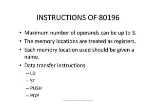
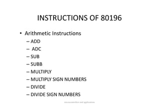
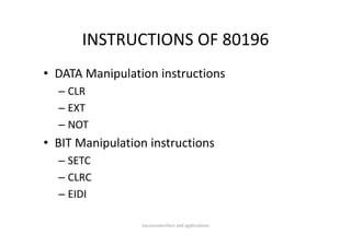
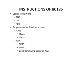
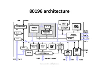
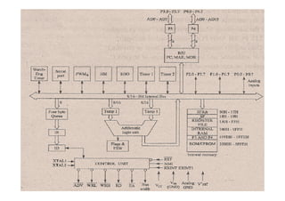
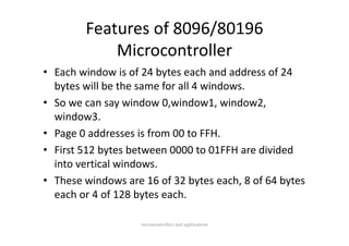
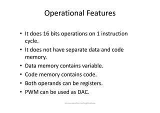
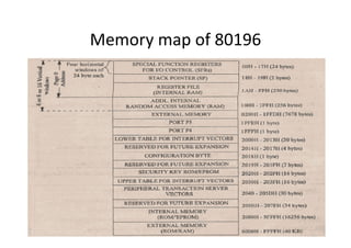
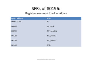
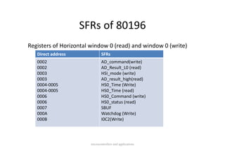
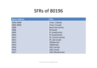
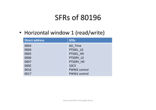
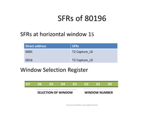
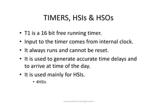
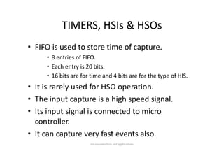
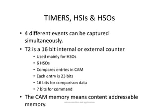
The document discusses the features and architecture of the 80196 microcontroller. It is a 16-bit microcontroller with a Princeton architecture that provides a continuous address space. It has various features like timers, serial ports, ADC, and PWM. The SFRs are located in the first 24 bytes of memory and are divided into horizontal windows. Interrupts are prioritized into 18 groups. The microcontroller supports various addressing modes and instruction types for arithmetic, logic, and program flow operations.

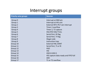
![ADDRESSING MODES
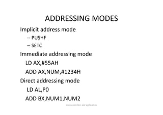
ADDRESSING MODES
Indirect addressing mode
Without port increment
Without port increment
– LD AX,[SI]
With post increment
– LD AX,[SI]+
[ ]
Index Long
– LD AX [SI ff t]
LD AX,[SI+offset]
Index short
– LD AX,DISP[SI] microcontrollers and applications](https://image.slidesharecdn.com/mcapptunitvii-111124071714-phpapp01/85/Mcapptunitvii-24-320.jpg)