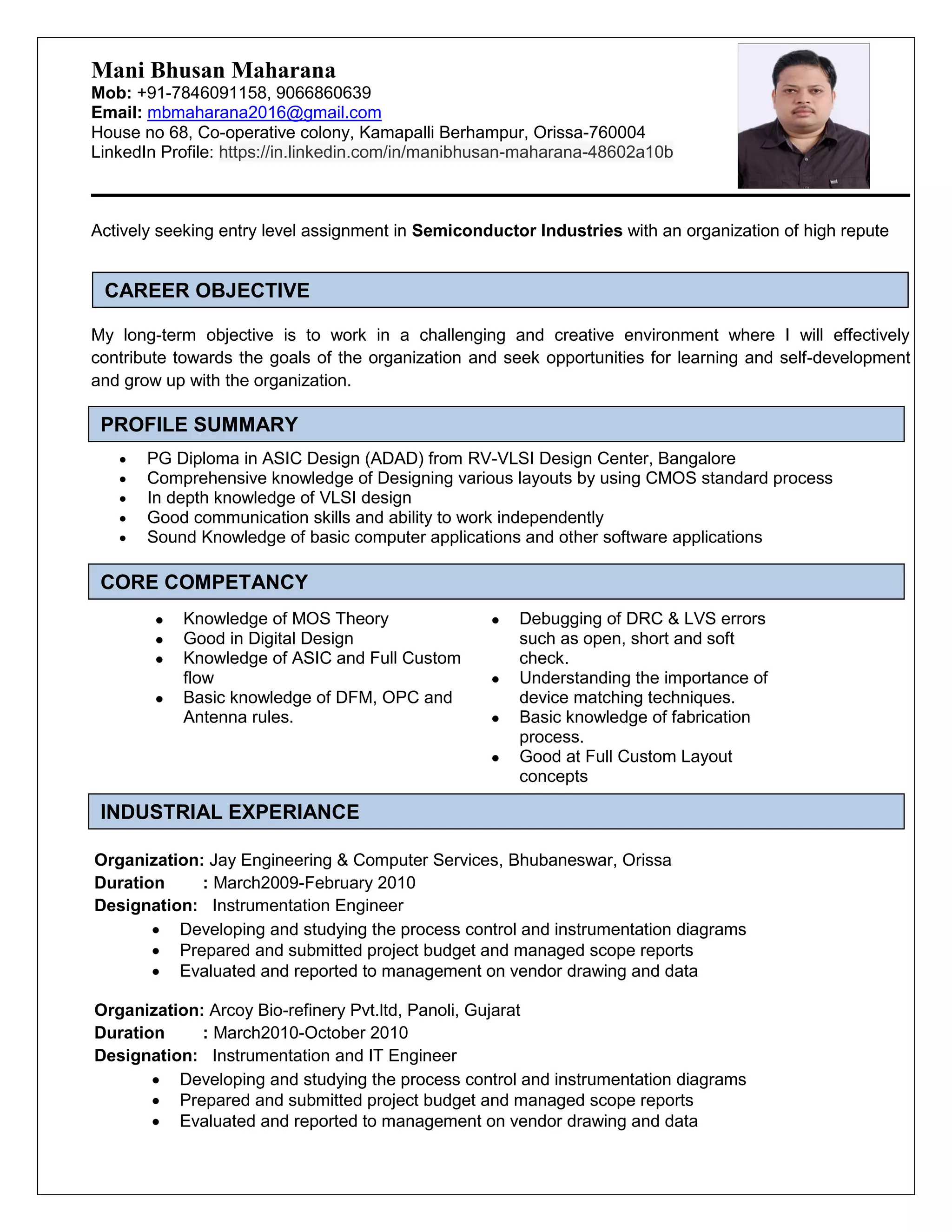
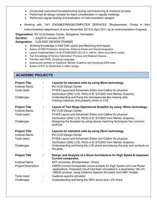
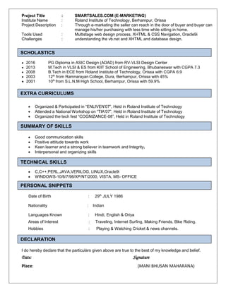
Mani Bhusan Maharana
Mob: +91-7846091158, 9066860639
Email: mbmaharana2016@gmail.com
House no 68, Co-operative colony, Kamapalli Berhampur, Orissa-760004
LinkedIn Profile: https://in.linkedin.com/in/manibhusan-maharana-48602a10b
Actively seeking entry level assignment in Semiconductor Industries with an organization of high repute
My long-term objective is to work in a challenging and creative environment where I will effectively
contribute towards the goals of the organization and seek opportunities for learning and self-development
and grow up with the organization.
Profile Summary
 PG Diploma in ASIC Design (ADAD) from RV-VLSI Design Center, Bangalore
 Comprehensive knowledge of Designing various layouts by using CMOS standard process
 In depth knowledge of VLSI design
 Good communication skills and ability to work independently
 Sound Knowledge of basic computer applications and other software applications
Core Competency
 Knowledge of MOS Theory
 Good in Digital Design
 Knowledge of ASIC and Full Custom
flow
 Basic knowledge of DFM, OPC and
Antenna rules.
 Debugging of DRC & LVS errors
such as open, short and soft
check.
 Understanding the importance of
device matching techniques.
 Basic knowledge of fabrication
process.
 Good at Full Custom Layout
concepts
Professional Experience
Organization: Jay Engineering & Computer Services, Bhubaneswar, Orissa
Duration : March2009-February 2010
Designation: Instrumentation Engineer
 Developing and studying the process control and instrumentation diagrams
 Prepared and submitted project budget and managed scope reports
 Evaluated and reported to management on vendor drawing and data
Organization: Arcoy Bio-refinery Pvt.ltd, Panoli, Gujarat
Duration : March2010-October 2010
Designation: Instrumentation and IT Engineer
 Developing and studying the process control and instrumentation diagrams
 Prepared and submitted project budget and managed scope reports
 Evaluated and reported to management on vendor drawing and data
CAREER OBJECTIVE
PROFILE SUMMARY
CORE COMPETANCY
INDUSTRIAL EXPERIANCE
 Conducted instrument troubleshooting during commissioning & checkout process
 Performed all design reviews for team consideration in regular meetings
 Performed regular testing and evaluation of instrumentation designs
 Working with “JAY ENGINEERING&COMPUTER SERVICES “Bhubaneswar, Orissa in their
Instrumentation department of since November 2010 to April 2011 as an Instrumentation Engineer.
Organization: RV-VLSI Design Center, Bangalore, Karnataka
Duration : July2015-January 2016
Designation: VLSI ASIC DESIGN TRAINEE
 Working knowledge in Half Cell Layout and Matching techniques.
 Aware of ESD Protection Schemes, Antenna Diode and Electronmigration.
 Layout Implementation of all STANDARD CELLS in 180nm, 90nm and 28nm nodes.
 Fair Knowledge of Device Fabrication Process and Relevant Issues.
 Familiar with PERL Scripting Language.
 Extensively worked on Cadence, Mentor Graphics and Synopsys EDA tools.
 Aware of RTL to GDSII flow in ASIC design.
Academic Projects
Project Title : Layouts for standard cells by using 90nm technology
Institute Name : RV-VLSI Design Center
Tools Used : PYXIS Layout and Schematic Editor and Calibre for physical
Verification (DRC LVS, PEX) in IC STUDIO from Mentor Graphics
Challenges : Understanding and fixing the discrepancies like missing nets,
missing instances and property errors in LVS
Project Title : Layout of Two Stage Operational Amplifier by using 180nm technology.
Institute Name : RV-VLSI Design Center
Tools Used : PYXIS Layout and Schematic Editor and Calibre for physical
Verification (DRC LVS, PEX) in IC STUDIO from Mentor Graphics
Challenges : Designing the floorplan by using device matching techniques like common
centroid.
Project Title : Layouts for standard cells by using 28nm technology.
Institute Name : RV-VLSI Design Center
Tools Used : PYXIS Layout and Schematic Editor and Calibre for physical
Verification (DRC LVS, PEX) in IC STUDIO from Mentor Graphics
Challenges : Understanding and fixing the LVS check and placing the poly and contacts on
the grids.
Project Title : Design and Analysis of a Novel Architecture for High Speed & lowpower
Current comparator.
Institute Name : KIIT University, Bhubaneswar, Orissa
Project Description : CMOS Current Comparator circuit suitable for High Speed and Low Power
applications. Proposed circuit had been simulated in a proprietary 180 nm
CMOS process, using Cadence Spectre Simulator and UMC models.
Tools Used : Cadence spectre simulator
Challenges : Understanding and fixing the DRC errors and LVS check
ACADEMIC PROJECTS
Project Title : SMARTSALES.COM (E-MARKETING)
Institute Name : Roland Institute of Technology, Berhampur, Orissa
Project Description : Through e-marketing the seller can reach in the door of buyer and buyer can
manage his/her purchasing with less time while sitting in home.
Tools Used : Multistage web design process, XHTML & CSS Navigation, Oracle9i
Challenges : understanding the vb.net and XHTML and database design.
Scholastic
2016 PG Diploma in ASIC Design (ADAD) from RV-VLSI Design Center
2013 M.Tech in VLSI & ES from KIIT School of Engineering, Bhubaneswar with CGPA 7.3
2008 B.Tech in ECE from Roland Institute of Technology, Orissa with CGPA 6.9
2003 12th
from Ramnarayan College, Dura, Berhampur, Orissa with 45%
2001 10th
from S.L.N.M High School, Berhampur, Orissa with 59.9%
Extra Curriculum
 Organized & Participated in “ENLIVEN’07”, Held in Roland Institute of Technology
 Attended a National Workshop on “TIA’07”, Held in Roland Institute of Technology
 Organized the tech fest “COGNIZANCE-08”, Held in Roland Institute of Technology
Summary of Skills
 Good communication skills
 Positive attitude towards work
 Keen learner and a strong believer in teamwork and Integrity.
 Interpersonal and organizing skills
Technical Skills
 C,C++,PERL,JAVA,VERILOG, LINUX,Oracle9i
 WINDOWS-10/8/7/98/XP/NT/2000, VISTA, MS- OFFICE
Personal Snippets
Date of Birth : 29th
JULY 1986
Nationality : Indian
Languages Known : Hindi, English & Oriya
Areas of Interest : Traveling, Internet Surfing, Making Friends, Bike Riding.
Hobbies : Playing & Watching Cricket & news channels.
Declaration
I do hereby declare that the particulars given above are true to the best of my knowledge and belief.
Date: Signature
Place: (MANI BHUSAN MAHARANA)
SCHOLASTICS
EXTRA CURRICULUMS
SUMMARY OF SKILLS
TECHNICAL SKILLS
PERSONAL SNIPPETS
DECLARATION

Mani Final Resume

  • 1.
    Mani Bhusan Maharana Mob:+91-7846091158, 9066860639 Email: mbmaharana2016@gmail.com House no 68, Co-operative colony, Kamapalli Berhampur, Orissa-760004 LinkedIn Profile: https://in.linkedin.com/in/manibhusan-maharana-48602a10b Actively seeking entry level assignment in Semiconductor Industries with an organization of high repute My long-term objective is to work in a challenging and creative environment where I will effectively contribute towards the goals of the organization and seek opportunities for learning and self-development and grow up with the organization. Profile Summary  PG Diploma in ASIC Design (ADAD) from RV-VLSI Design Center, Bangalore  Comprehensive knowledge of Designing various layouts by using CMOS standard process  In depth knowledge of VLSI design  Good communication skills and ability to work independently  Sound Knowledge of basic computer applications and other software applications Core Competency  Knowledge of MOS Theory  Good in Digital Design  Knowledge of ASIC and Full Custom flow  Basic knowledge of DFM, OPC and Antenna rules.  Debugging of DRC & LVS errors such as open, short and soft check.  Understanding the importance of device matching techniques.  Basic knowledge of fabrication process.  Good at Full Custom Layout concepts Professional Experience Organization: Jay Engineering & Computer Services, Bhubaneswar, Orissa Duration : March2009-February 2010 Designation: Instrumentation Engineer  Developing and studying the process control and instrumentation diagrams  Prepared and submitted project budget and managed scope reports  Evaluated and reported to management on vendor drawing and data Organization: Arcoy Bio-refinery Pvt.ltd, Panoli, Gujarat Duration : March2010-October 2010 Designation: Instrumentation and IT Engineer  Developing and studying the process control and instrumentation diagrams  Prepared and submitted project budget and managed scope reports  Evaluated and reported to management on vendor drawing and data CAREER OBJECTIVE PROFILE SUMMARY CORE COMPETANCY INDUSTRIAL EXPERIANCE
  • 2.
     Conducted instrumenttroubleshooting during commissioning & checkout process  Performed all design reviews for team consideration in regular meetings  Performed regular testing and evaluation of instrumentation designs  Working with “JAY ENGINEERING&COMPUTER SERVICES “Bhubaneswar, Orissa in their Instrumentation department of since November 2010 to April 2011 as an Instrumentation Engineer. Organization: RV-VLSI Design Center, Bangalore, Karnataka Duration : July2015-January 2016 Designation: VLSI ASIC DESIGN TRAINEE  Working knowledge in Half Cell Layout and Matching techniques.  Aware of ESD Protection Schemes, Antenna Diode and Electronmigration.  Layout Implementation of all STANDARD CELLS in 180nm, 90nm and 28nm nodes.  Fair Knowledge of Device Fabrication Process and Relevant Issues.  Familiar with PERL Scripting Language.  Extensively worked on Cadence, Mentor Graphics and Synopsys EDA tools.  Aware of RTL to GDSII flow in ASIC design. Academic Projects Project Title : Layouts for standard cells by using 90nm technology Institute Name : RV-VLSI Design Center Tools Used : PYXIS Layout and Schematic Editor and Calibre for physical Verification (DRC LVS, PEX) in IC STUDIO from Mentor Graphics Challenges : Understanding and fixing the discrepancies like missing nets, missing instances and property errors in LVS Project Title : Layout of Two Stage Operational Amplifier by using 180nm technology. Institute Name : RV-VLSI Design Center Tools Used : PYXIS Layout and Schematic Editor and Calibre for physical Verification (DRC LVS, PEX) in IC STUDIO from Mentor Graphics Challenges : Designing the floorplan by using device matching techniques like common centroid. Project Title : Layouts for standard cells by using 28nm technology. Institute Name : RV-VLSI Design Center Tools Used : PYXIS Layout and Schematic Editor and Calibre for physical Verification (DRC LVS, PEX) in IC STUDIO from Mentor Graphics Challenges : Understanding and fixing the LVS check and placing the poly and contacts on the grids. Project Title : Design and Analysis of a Novel Architecture for High Speed & lowpower Current comparator. Institute Name : KIIT University, Bhubaneswar, Orissa Project Description : CMOS Current Comparator circuit suitable for High Speed and Low Power applications. Proposed circuit had been simulated in a proprietary 180 nm CMOS process, using Cadence Spectre Simulator and UMC models. Tools Used : Cadence spectre simulator Challenges : Understanding and fixing the DRC errors and LVS check ACADEMIC PROJECTS
  • 3.
    Project Title :SMARTSALES.COM (E-MARKETING) Institute Name : Roland Institute of Technology, Berhampur, Orissa Project Description : Through e-marketing the seller can reach in the door of buyer and buyer can manage his/her purchasing with less time while sitting in home. Tools Used : Multistage web design process, XHTML & CSS Navigation, Oracle9i Challenges : understanding the vb.net and XHTML and database design. Scholastic 2016 PG Diploma in ASIC Design (ADAD) from RV-VLSI Design Center 2013 M.Tech in VLSI & ES from KIIT School of Engineering, Bhubaneswar with CGPA 7.3 2008 B.Tech in ECE from Roland Institute of Technology, Orissa with CGPA 6.9 2003 12th from Ramnarayan College, Dura, Berhampur, Orissa with 45% 2001 10th from S.L.N.M High School, Berhampur, Orissa with 59.9% Extra Curriculum  Organized & Participated in “ENLIVEN’07”, Held in Roland Institute of Technology  Attended a National Workshop on “TIA’07”, Held in Roland Institute of Technology  Organized the tech fest “COGNIZANCE-08”, Held in Roland Institute of Technology Summary of Skills  Good communication skills  Positive attitude towards work  Keen learner and a strong believer in teamwork and Integrity.  Interpersonal and organizing skills Technical Skills  C,C++,PERL,JAVA,VERILOG, LINUX,Oracle9i  WINDOWS-10/8/7/98/XP/NT/2000, VISTA, MS- OFFICE Personal Snippets Date of Birth : 29th JULY 1986 Nationality : Indian Languages Known : Hindi, English & Oriya Areas of Interest : Traveling, Internet Surfing, Making Friends, Bike Riding. Hobbies : Playing & Watching Cricket & news channels. Declaration I do hereby declare that the particulars given above are true to the best of my knowledge and belief. Date: Signature Place: (MANI BHUSAN MAHARANA) SCHOLASTICS EXTRA CURRICULUMS SUMMARY OF SKILLS TECHNICAL SKILLS PERSONAL SNIPPETS DECLARATION