1. The document discusses the structure, operation, and characteristics of silicon controlled rectifiers (SCRs). SCRs are semiconductor devices that act as electrically controlled switches.
2. The key aspects covered include the two-transistor model of an SCR, conditions for turn on and turn off, factors affecting turn on such as voltage and temperature, and methods of turning off an SCR.
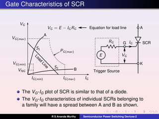
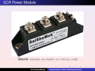
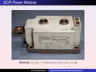
3. Design considerations for SCRs like snubber circuits, gate protection, and turn on/off characteristics are also summarized. Different packages for SCRs like disc, stud, and power modules are shown along with specifications.


![Conditions for Turn ON and Turn OFF of SCR
In Figure-(c) of previous slide, by applying KCL to the device we
get
IK = IA +IG and IA = IC1 +IC2 (1)
Considering each transistor we have
IC1 = α1IA +ICBO1 and IC2 = α2IK +ICBO2 (2)
Substituting Eq.(2) in (1) and by rearranging terms we get
IA =
α2IG +(ICBO1 +ICBO2)
[1−(α1 +α2)]
(3)
When (α1 +α2) << 1 the device is OFF as IA ≈ (ICBO1 +ICBO2).
When (α1 +α2) → 1 the device turns ON since IA → ∞.
R S Ananda Murthy Semiconductor Power Switching Devices-2](https://image.slidesharecdn.com/l5-semiconductor-power-switching-devices-2-130818121609-phpapp01-150419144053-conversion-gate01/85/L5-semiconductor-power-switching-devices-2-130818121609-phpapp01-5-320.jpg)