
Recommended
More Related Content
Similar to Know about basic logic gates with truth tables
Similar to Know about basic logic gates with truth tables (20)
Recently uploaded
Recently uploaded (20)
Know about basic logic gates with truth tables
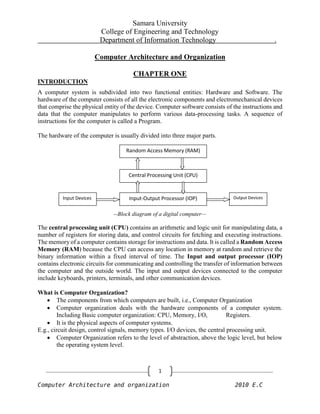
- 1. Samara University College of Engineering and Technology Department of Information Technology . Computer Architecture and organization 2010 E.C 1 Computer Architecture and Organization CHAPTER ONE INTRODUCTION A computer system is subdivided into two functional entities: Hardware and Software. The hardware of the computer consists of all the electronic components and electromechanical devices that comprise the physical entity of the device. Computer software consists of the instructions and data that the computer manipulates to perform various data-processing tasks. A sequence of instructions for the computer is called a Program. The hardware of the computer is usually divided into three major parts. --Block diagram of a digital computer— The central processing unit (CPU) contains an arithmetic and logic unit for manipulating data, a number of registers for storing data, and control circuits for fetching and executing instructions. The memory of a computer contains storage for instructions and data. It is called a Random Access Memory (RAM) because the CPU can access any location in memory at random and retrieve the binary information within a fixed interval of time. The Input and output processor (IOP) contains electronic circuits for communicating and controlling the transfer of information between the computer and the outside world. The input and output devices connected to the computer include keyboards, printers, terminals, and other communication devices. What is Computer Organization? The components from which computers are built, i.e., Computer Organization Computer organization deals with the hardware components of a computer system. Including Basic computer organization: CPU, Memory, I/O, Registers. It is the physical aspects of computer systems. E.g., circuit design, control signals, memory types. I/O devices, the central processing unit. Computer Organization refers to the level of abstraction, above the logic level, but below the operating system level. Random Access Memory (RAM) Central Processing Unit (CPU) Input-Output Processor (IOP)Input Devices Output Devices
- 2. Samara University College of Engineering and Technology Department of Information Technology . Computer Architecture and organization 2010 E.C 2 The major components at this level are subsystems, or functional units, which correspond to particular hardware pieces. The operational units and their interconnections that realize the architectural specifications. It is concerned with the way the hardware components operate and the way they are connected together to form the computer system. Those hardware attributes that are transparent to the programmer. Computer Architecture Computer architecture refers to engineering considerations that are useful in coming up with a desirable computer design. Computer architecture is the science of integrating those components to achieve a level of functionality and performance. It is the Logical aspects of system as seen by the programmer. E.g., instruction sets, instruction formats, data types, addressing modes. Those attributes of the system that is visible to a programmer. It is concerned with the structure and behavior of the computer as seen by the user. Those attributes that have a direct impact on the execution of a program. • Instruction sets • Data representation – number of bits used to represent data • Input/output mechanisms • Memory addressing techniques Computer Design It is concerned with hardware design of the computer. Once the computer specifications are formulated, it is the task of the designer to develop hardware for the system. This is sometimes referred to as computer implementation. Know about Basic Logic Gates with Truth Tables Nowadays, computers have become an integral part of life as they perform many tasks and operations in quite a short span of time. One of the most important functions of the CPU in a computer is to perform logical operations by utilizing hardware like Integrated Circuits, electronic circuits and software technologies. But, how these hardware and software perform such operations is a mysterious puzzle. In order to have a better understanding of such a complex issue, we must have to acquaint ourselves with the term Boolean Logic, developed by George Boole. For a simple
- 3. Samara University College of Engineering and Technology Department of Information Technology . Computer Architecture and organization 2010 E.C 3 operation, computers utilize binary digits rather than digital digits. All the operations are carried out by the Basic Logic gates. Basic Logic Gates What is Logic Gate? A logic gate is a basic building block of a digital circuit that has two inputs and one output. The relationship between the input and the output is based on a certain logic. These gates are implemented using electronic switches like transistors, diodes. But, in practice basic logic gates are built using CMOS technology, FETS and MOSFET (Metal Oxide Semiconductor FET)s. Logic gates are used in microprocessors, microcontrollers, and embedded system applications and in electronic and electrical project circuits. The basic logic gates are categorized into seven: AND, OR, XOR, NAND, NOR, XNOR and NOT. These logic gates with their logic gate symbols and truth tables are explained below. Logic Gate AND Gate The AND gate is a digital logic gate with ‘n’ inputs one output, which perform logical conjunction based on the combinations of its inputs. The output of this gate is true only when all the inputs are
- 4. Samara University College of Engineering and Technology Department of Information Technology . Computer Architecture and organization 2010 E.C 4 true. When one or more inputs of the AND gate’s inputs are false, then only the output of the AND gate is false. The symbol, function and truth table of an AND gate with two inputs is shown below. OR Gate The OR gate is a digital logic gate with ‘n’ inputs and one output, that performs a logical conjunction based on the combinations of its inputs. The output of the OR gate is true only when one or more inputs are true. If all the inputs of the gate are false, then only the output of the OR gate is false. The symbol, function and truth table of an OR gate with two inputs is shown below. NOT Gate The NOT gate is a digital logic gate with one input and one output that operates an inverter operation of the input. The output of the NOT gate is the reverse of the input. When the input of the NOT gate is true then the output will be false and vice versa. The symbol, function and truth table of a NOT gate with one input is shown below. By using this gate, we can implement NOR and NAND gates
- 5. Samara University College of Engineering and Technology Department of Information Technology . Computer Architecture and organization 2010 E.C 5 NAND Gate The NAND gate is a digital logic gate with ‘n’ inputs and one output, that performs the operation of the AND gate followed by the operation of the NOT gate. NAND gate is designed by combining the AND and NOT gates. If the input of the NAND gate high, then the output of the gate will be low. The symbol, function and truth table of the NAND gate with two inputs is shown below. NOR Gate The NOR gate is a digital logic gate with n inputs and one output, that performs the operation of the OR gate followed by the NOT gate. NOR gate is designed by combining the OR and NOT gate. When any one of the inputs of the NOR gate is true, then the output of the NOR gate will be false. The symbol, function and truth table of the NOR gate with truth table is shown below. Exclusive-OR Gate The Exclusive-OR gate is a digital logic gate with two inputs and one output. The short form of this gate is Ex-OR. It performs based on the operation of OR gate. . If any one of the inputs of this gate is high, then the output of the EX-OR gate will be high. The symbol, function and truth table of the EX-OR are shown below.
- 6. Samara University College of Engineering and Technology Department of Information Technology . Computer Architecture and organization 2010 E.C 6 Exclusive-NOR Gate The Exclusive-NOR gate is a digital logic gate with two inputs and one output. The short form of this gate is Ex-NOR. It performs based on the operation of NOR gate. When both the inputs of this gate are high, then the output of the EX-NOR gate will be high. But, if any one of the inputs is high (but not both), then the output will be low. The symbol, function and truth table of the EX- NOR are shown below. The applications of logic gates are mainly determined based upon their truth table, i.e., their mode of operations. The basic logic gates are used in many circuits like a push-button lock, light- activated burglar alarm, safety thermostat, an automatic watering system, etc. By using mixtures of basic logic gates, advanced operations are often performed. In theory, there’s no limit to the quantity of gates that may be clad along during a single device. However, in application, there’s a limit to the quantity of gates that may be packed into a given physical area. Arrays of the logic gate area unit are found in digital integrated circuits (ICs). As IC technology advances, the desired physical volume for every individual gate decreases and digital devices of an equivalent or smaller size become capable of activity with more complicated operations at ever-increasing speeds. This is all about the basic logic gates, which includes AND gate, OR gate, NAND gate, NOR gate, EX-OR gate and EX-NOR gate. In this, AND, NOT and OR gates are the basic logic gates. By using these gates we can create any logic gate by combining them. Where, NAND and NOR gates Note Function O = A’B +AB’ Note Function O = A’B +AB’
- 7. Samara University College of Engineering and Technology Department of Information Technology . Computer Architecture and organization 2010 E.C 7 are called universal gates. These gates have a particular property with which they can create any logical Boolean expression if designed in a proper way. List of Logic Gate Integrated Circuit (Ics) There are different Integrated Circuit (IC) technologies are used to implement the basic logic gates ICs CMOS TTL ECL They are CMOS (Complementary Metal – Oxide Semiconductor), TTL (Transistor – Transistor Logic) and ECL (Emitter – Coupled Logic). Simplification of Logic Circuit Design Boolean Algebra Karnaugh map (k-map) Boolean Algebra Boolean algebra is mathematical system for formulating logical statements with symbols so that problems can be solved in a manner to ordinary algebra. Boolean algebra is the mathematics of digital systems A basic knowledge in the Boolean algebra required to study and analysis of logic circuits. It is a convenient and systematic way of expressing and analyzing the operations of logic circuits. Rule Number Boolean Expression 1 A + 0 = A 2 A + 1 = 1 3 A. 0 = 0 4 A.1 =A 5 A + A = A 6 A + Ā = 1 7 A .A = A 8 A. Ā =0 9 Ā=A 10 A + AB =A
- 8. Samara University College of Engineering and Technology Department of Information Technology . Computer Architecture and organization 2010 E.C 8 11 A +A B = A + B 12 (A + B) (A + C) = A + BC Commutative Law : A + B = B + A AB = BA Associative Law : A+(B+C) = (A+B)+C A(BC) = (AB)C Distributive law: A(B+C) = AB + AC A +(BC) = (A+B). (A+C) De morgan’sTheorems : A + B = A . B A.B = A + B Let see the following give Boolean functions. For example, for the Boolean functions examples. Example1: simplify Y= + This can be verified algebraically as follows: Y= + = ( + A) = Example 2: simplify Y= + AB + Verifying the problems algebraically as follows: Y= + AB + = + AB + AB + = ( + A) + A (B+B) = B + A A B A B A B A B B A B A BA B A BA B A BA B AB
- 9. Samara University College of Engineering and Technology Department of Information Technology . Computer Architecture and organization 2010 E.C 9 K-Map K-map is developed by telecommunication engineer More easier and simpler than Boolean Steps to simplify using k-map Prepare truth table depending on the inputs and Gray code rule Place 1’s in a truth table for each part of expressions and other left blank Encircle adjacent 1’s to form a large group by power of two amount; double encircle of a cell or cells is possible if the cell again adjacent for next group Take the common in a circle and if you have more than one circle add the groups result Gray code generation rule : Example
- 10. Samara University College of Engineering and Technology Department of Information Technology . Computer Architecture and organization 2010 E.C 10 Above we, place the 1’s in the K-map for each of the product terms, identify a group of two, then write a p-term (product term) for the sole group as our simplified result. Eample2: Mapping the four product terms above yields a group of four covered by Boolean A’ Eample3: Mapping the four p-terms yields a group of four, which is covered by one variable C. Exmple4: After mapping the six p-terms above, identify the upper group of four, pick up the lower two cells as a group of four by sharing the two with two more from the other group. Covering these two with a group of four gives a simpler result. Since there are two groups, there will be two p-terms in the Sum-of-Products result A’+B
- 11. Samara University College of Engineering and Technology Department of Information Technology . Computer Architecture and organization 2010 E.C 11 Eample5: The two product terms above form one group of two and simplifies to BC Eample6: Mapping the four p-terms yields a single group of four, which is B Eample7: Mapping the four p-terms above yields a group of four. Visualize the group of four by rolling up the ends of the map to form a cylinder, then the cells are adjacent. We normally mark the group of four as above left. Out of the variables A, B, C, there is a common variable: C’. C’ is a 0 over all four cells. Final result is C’.
- 12. Samara University College of Engineering and Technology Department of Information Technology . Computer Architecture and organization 2010 E.C 12 Exmple8: The six cells above from the unsimplified equation can be organized into two groups of four. These two groups should give us two p-terms in our simplified result of A’ + C’. Four Variables Expression Simplification using k-map Knowing how to generate Gray code should allow us to build larger maps. Actually, all we need to do is look at the left to right sequence across the top of the 3-variable map, and copy it down the left side of the 4-variable map. See below. The following four variable Karnaugh maps illustrate reduction of Boolean expressions too tedious for Boolean algebra. Reductions could be done with Boolean algebra. However, the Karnaugh map is faster and easier, especially if there are many logic reductions to do. Exmple9: The above Boolean expression has seven product terms. They are mapped top to bottom and left to right on the K-map above. For example, the first P-term A’B’CD is first row 3rd cell, corresponding to map location A=0, B=0, C=1, D=1. The other product terms are placed in a
- 13. Samara University College of Engineering and Technology Department of Information Technology . Computer Architecture and organization 2010 E.C 13 similar manner. Encircling the largest groups possible, two groups of four are shown above. The dashed horizontal group corresponds the the simplified product term AB. The vertical group corresponds to Boolean CD. Since there are two groups, there will be two product terms in the Sum-Of-Products result of Out=AB+CD. Fold up the corners of the map below like it is a napkin to make the four cells physically adjacent. Exmple10: The four cells above are a group of four because they all have the Boolean variables B’ and D’ in common. In other words, B=0 for the four cells, and D=0 for the four cells. The other variables (A, C) are 0 in some cases, 1 in other cases with respect to the four corner cells. Thus, these variables (A, C) are not involved with this group of four. This single group comes out of the map as one product term for the simplified result: Out=B’D’ For the K-map below, roll the top and bottom edges into a cylinder forming eight adjacent cells. Example11: The above group of eight has one Boolean variable in common: B=0. Therefore, the one group of eight is covered by one p-term: B’. The original eight term Boolean expression simplifies to Out=B’ The Boolean expression below has nine p-terms, three of which have three Booleans instead of four. The difference is that while four Boolean variable product terms cover one cell, the three Boolean p-terms cover a pair of cells each.
- 14. Samara University College of Engineering and Technology Department of Information Technology . Computer Architecture and organization 2010 E.C 14 Example12: The six product terms of four Boolean variables map in the usual manner above as single cells. The three Boolean variable terms (three each) map as cell pairs, which is shown above. Note that we are mapping p-terms into the K-map, not pulling them out at this point. For the simplification, we form two groups of eight. Cells in the corners are shared with both groups. This is fine. In fact, this leads to a better solution than forming a group of eight and a group of four without sharing any cells. Final Solution is Out=B’+D’ Below we map the unsimplified Boolean expression to the Karnaugh map. Example13:
- 15. Samara University College of Engineering and Technology Department of Information Technology . Computer Architecture and organization 2010 E.C 15 Above, three of the cells form into a groups of two cells. A fourth cell cannot be combined with anything, which often happens in “real world” problems. In this case, the Boolean p- term ABCD is unchanged in the simplification process. Result: Out= B’C’D’+A’B’D’+ABCD Often times there is more than one minimum cost solution to a simplification problem. Such is the case illustrated below. Example14: Both results above have four product terms of three Boolean variable each. Both are equally valid minimal cost solutions. The difference in the final solution is due to how the cells are grouped as shown above. A minimal cost solution is a valid logic design with the minimum number of gates with the minimum number of inputs. Example15: Below we map the unsimplified Boolean equation as usual and form a group of four as a first simplification step. It may not be obvious how to pick up the remaining cells.
- 16. Samara University College of Engineering and Technology Department of Information Technology . Computer Architecture and organization 2010 E.C 16 Pick up three more cells in a group of four, center above. There are still two cells remaining. the minimal cost method to pick up those is to group them with neighboring cells as groups of four as at above right. Product of Sum and Sum of Product So far we have seen product of sum expressions like and each terms are called minterm Which means addition of product terms and also how to simplify this expressions. There is the revers expression also sum of product like this If this happens the simplification way is different and you have to use the following steps: Identify the Sum term to be mapped. Write corresponding binary numeric value. Form the complement Use the complement as an address to place a 0 in the K-map Repeat for other maxterms (Sum terms within Product-of-Sums expression). Example A Boolean Product-Of-Sums expression or map may have multiple maxterms as shown above. Maxterm (A+B+C) yields numeric 111 which complements to 000, placing a 0 in cell (0,0,0). Maxterm (A+B+C’) yields numeric 110 which complements to 001, placing a 0 in cell (0,0,1). Now that we have the k-map setup, what we are really interested in is showing how to write a Product-Of-Sums reduction. Form the 0s into groups. That would be a group of two below. Write the binary value corresponding to the sum-term which is (0,0,X). Both A and B are 0 for
- 17. Samara University College of Engineering and Technology Department of Information Technology . Computer Architecture and organization 2010 E.C 17 the group. But, C is both 0 and 1 so we write an X as a place holder for C. Form the complement (1,1,X). Write the Sum-term (A+B) discarding the C and the X which held its’ place. In general, expect to have more sum-terms multiplied together in the Product-Of-Sums result. Though, we have a simple example here. Example 2 Solution: Transfer the seven maxterms to the map below as 0s. Be sure to complement the input variables in finding the proper cell location. We map the 0s as they appear left to right top to bottom on the map above. We locate the last three maxterms with leader lines.. Once the cells are in place above, form groups of cells as shown below. Larger groups will give a sum-term with fewer inputs. Fewer groups will yield fewer sum-terms in the result.
- 18. Samara University College of Engineering and Technology Department of Information Technology . Computer Architecture and organization 2010 E.C 18 We have three groups, so we expect to have three sum-terms in our POS result above. The group of 4-cells yields a 2-variable sum-term. The two groups of 2-cells give us two 3-variable sum- terms. Details are shown for how we arrived at the Sum-terms above. For a group, write the binary group input address, then complement it, converting that to the Boolean sum-term. The final result is product of the three sums. Introduction to Logic Circuits The signals are usually represented by discrete bands of analog levels in digital electronic circuits or digital electronics instead of continuous ranges represented in analogue electronics. The simple electronic representations of Boolean logic functions, large assemblies of logic gates are typically used to make digital electronic circuits. In digital circuit theory, the circuits, thus formed from logic gates are used to generate outputs based on the input logic. Hence, these circuits are called as logic circuits and are classified into two types such as sequential logic and combinational logic circuits. Introduction to Logic Circuits
- 19. Samara University College of Engineering and Technology Department of Information Technology . Computer Architecture and organization 2010 E.C 19 Logic Circuits Combinational Logic Circuit Definition The combinational logic circuits or time-independent logic circuits in digital circuit theory can be defined as a type of digital logic circuit implemented using Boolean circuits, where the output of logic circuit is a pure function of the present inputs only. The combinational logic circuit operation is instantaneous and these circuits do not have the memory or feedback loops. This combinational logic is in contrast compared to the sequential logic circuit in which the output depends on both present inputs and also on the previous inputs. Thus, we can say that combinational logic does not have memory, whereas sequential logic stores previous input in its memory. Hence, if the input of combinational logic circuit changes, then the output also changes. Combinational Logic Circuit Design These combinational logic circuits are designed to produce specific outputs from certain inputs. The combinational logic design can be done using two methods such as a sum of products and a product of sums. Combinational logic circuits are generally designed by connecting together or combining the basic logic gates such as NAND, NOR, and NOT. Hence, these logic gates are termed as building blocks. These logic circuits can be a very simple circuit or a very complex
- 20. Samara University College of Engineering and Technology Department of Information Technology . Computer Architecture and organization 2010 E.C 20 circuit or huge combinational circuit can be designed using only universal logic gates such as NAND and NOR gates. The function of combinational logic circuits can be specified in three main ways such as: Truth Table Boolean Algebra Logic Diagram Combinational Logic Circuit using Logic Gates The graphical representation of combinational logic functions using logic gates is called as logic diagram. The combinational logic circuits can be also be called as decision making circuits, as these are designed using individual logic gates. The combinational logic is the process of combining logic gates to process the given two or more inputs such that to generate at least one output signal based on the logic function of each logic gate. Classification of Combinational Logic The combinational logic circuits can be classified into various types based on the purpose of usage, such as arithmetic & logical functions, data transmission, and code converters. To solve the
- 21. Samara University College of Engineering and Technology Department of Information Technology . Computer Architecture and organization 2010 E.C 21 arithmetic and logical functions we generally use adders, subtractors, and comparators which are generally realized by combining various logic gates called as combinational logic circuits. Similarly, for data transmission, we use multiplexers, demultiplexers, encoders, and decoders which are also realized using combinational logic. The code converters such as binary, BCD, and 7-segment are designed using various logic circuits. In fact, combinational logic is most frequently used in multiplexer and demultiplexer type circuits. If multiple inputs or outputs are connected to the common signal line, then the logic gates are used for decoding an address in order to select single data input or output switch. Introduction to Sequential Logic Circuits A Sequential logic circuits is a form of binary circuit; its design employs one or more inputs and one or more outputs, whose states are related to some definite rules that depends on previous states. Both the inputs and outputs can reach either of the two states: logic 0 (low) or logic 1 (high). In these circuits their output depends, not only on the combination of the logic states at its inputs, but moreover on the logic states that existed previously. In other words their output depends on a SEQUENCE of the events occurring at the circuit inputs. Examples of such circuits include clocks, flip-flops, bi-stables, counters, memories, and registers. The actions of the circuits depend on the range of basic sub-circuits. What is a Sequential Logic Circuit? Dissimilar Combinational Logic circuits can change state depending on the real signals that are applied to their inputs, at the same time,Sequential Logic Circuits include some form of inherent “Memory” build into them as they are capable of taking into account their previous input state as well as the individuals really present, a sort of “before” and “after” effect is involved with the sequential logic circuits.A very simple sequential circuit with no inputs can be created using inverter to form a feedback loop
- 22. Samara University College of Engineering and Technology Department of Information Technology . Computer Architecture and organization 2010 E.C 22 Sequential Logic Circuit Block Diagram Types of Sequential Logic Circuits Differences between the Combinational and Sequential Logic Circuits Combinational circuits Sequential circuits The circuit whose output , at any immediate time, depends only on the input present at that instant only is known as combinational circuit. The circuit whose output at any immediate time depends not only on the input present, but also on the past output, is known as sequential circuit These types of circuits have no memory unit. These types of circuits have a memory unit to store past output. It is Faster. It is Slower. These are easy to design. These are difficult to design. Examples of combinational circuits are half adder, full adder, magnitude comparator, multiplexer, demultiplexer, etc. Examples of sequential circuits are flip-flop, register, counter, clocks, etc.
- 23. Samara University College of Engineering and Technology Department of Information Technology . Computer Architecture and organization 2010 E.C 23 Computer circuits consist of combinational logic circuits and sequential logic circuits. Combinational circuits produce outputs immediately when their input changes. Sequential circuits require clocks to control their changes of state. The fundamental sequential circuit unit is the flip- flop and the behavior of the SR, JK, and D flip-flops are the most important to know. Integrated Circuits(IC) Digital circuits are constructed with Integrated Circuits An Integrated Circuits is a small silicon semiconductor crystal, called chip The various gates are interconnected inside the chip to form the required circuit The chip is mounted in a ceramic or plastic container, and connections are welded by thin gold wires to external pins to form the integrated circuits The number of pins may range from 14 in a small IC package to 100 or more in a larger package Each IC has a numeric designation printed on the surface of the package for identification o SSI, MSI, LSI: They perform small tasks such as addition of few bits. small memories, small processors o VLSI Tasks: - Large memory - Complex microprocessors, CPUs