Download to read offline

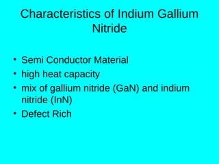


Indium gallium nitride (InGaN) is a semiconductor material made of a mixture of gallium nitride and indium nitride. It has advantages such as a low band gap of 0.7eV that can be tuned across the electromagnetic spectrum by adjusting composition. Additionally, it has a smooth band gap curve and can be easily made into layers due to its tolerance for mismatched lattice systems. However, it also has disadvantages like being difficult to dope to create p-type material and containing billions of defects per square centimeter.


