Downloaded 13 times


![Workshop_WMH
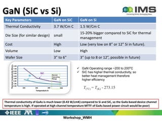
Why GaN
High Breakdown Field
10x of Si or GaAs
High Power Density
2-10x of Si or GaAs
Good Thermal Conductivity
Higher Impedances
Best Power Device Figure of Merit
Low Dielectric Constant
Lower Intrinsic Capacitances
JFM = Johnson's figure of merit is a measure of suitability of a semiconductor material
for high frequency power transistor applications and requirements
JFM=(Breakdown, electron velocity product) [Eb*Vbr/2π]
Highest Johnson Figure of Merit
Si=1.0, GaAs=2.7, SiC=20,
GaN=27.5](https://image.slidesharecdn.com/547da1fe-4acd-4df4-a298-6d42d95acd32-160801223630/85/IMS2016_Workshop_SK-03232016-29-320.jpg)


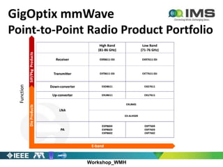
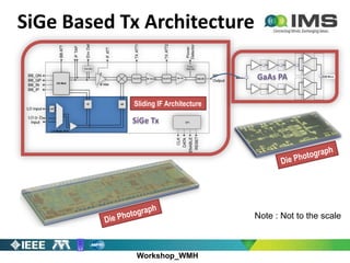
This document provides an overview of trade-offs in designing E-band transceiver monolithic microwave integrated circuits (MMICs) for gigabit wireless links. It discusses SiGe and GaAs semiconductor technologies that can be used for transmitter and receiver designs. Measured results are presented for SiGe-based transmitters showing output power, gain, and noise performance. Package options for E-band systems are also reviewed. The document concludes with a summary of how GaAs and SiGe technologies can be combined to achieve high performance while controlling costs for E-band transceiver designs.


![US8131248[1]](https://cdn.slidesharecdn.com/ss_thumbnails/28e09a69-fca7-4c5c-9043-e984dfde3d8c-161115001935-thumbnail.jpg?width=640&height=640&fit=bounds)