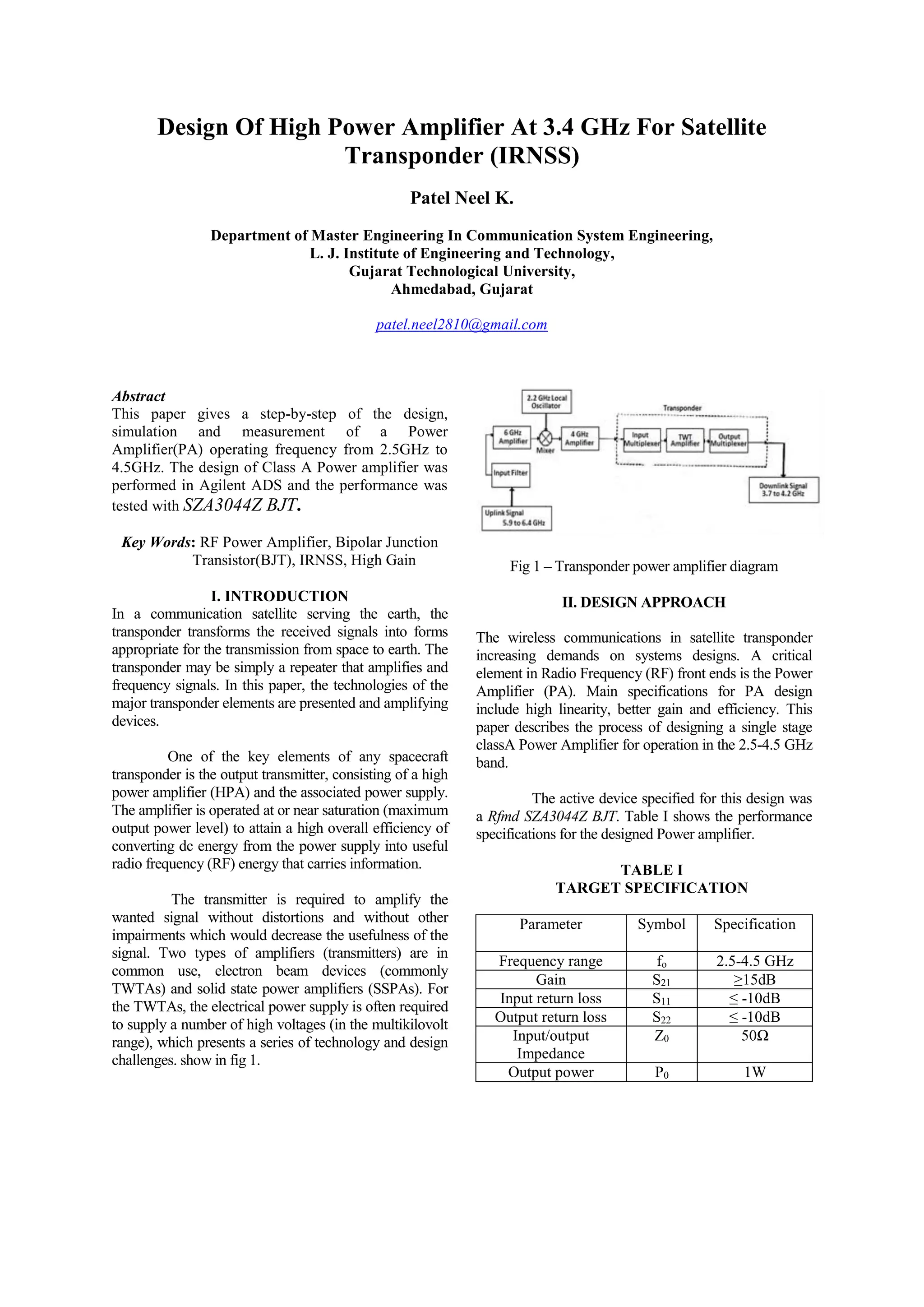
This document summarizes the design, simulation, and measurement of a class A power amplifier operating from 2.5GHz to 4.5GHz for use in satellite transponders. The power amplifier was designed using a SZA3044Z BJT transistor in Agilent ADS. Stability and impedance matching networks were designed to maximize gain and minimize reflections. Measurements showed a gain of 26.4dB, input return loss better than -39.8dB, and output return loss better than -49.3dB, meeting most but not all specifications. While improvements are needed, the design process provided insight into challenges in high power amplifier design.
![Fig 11- S21 Gain
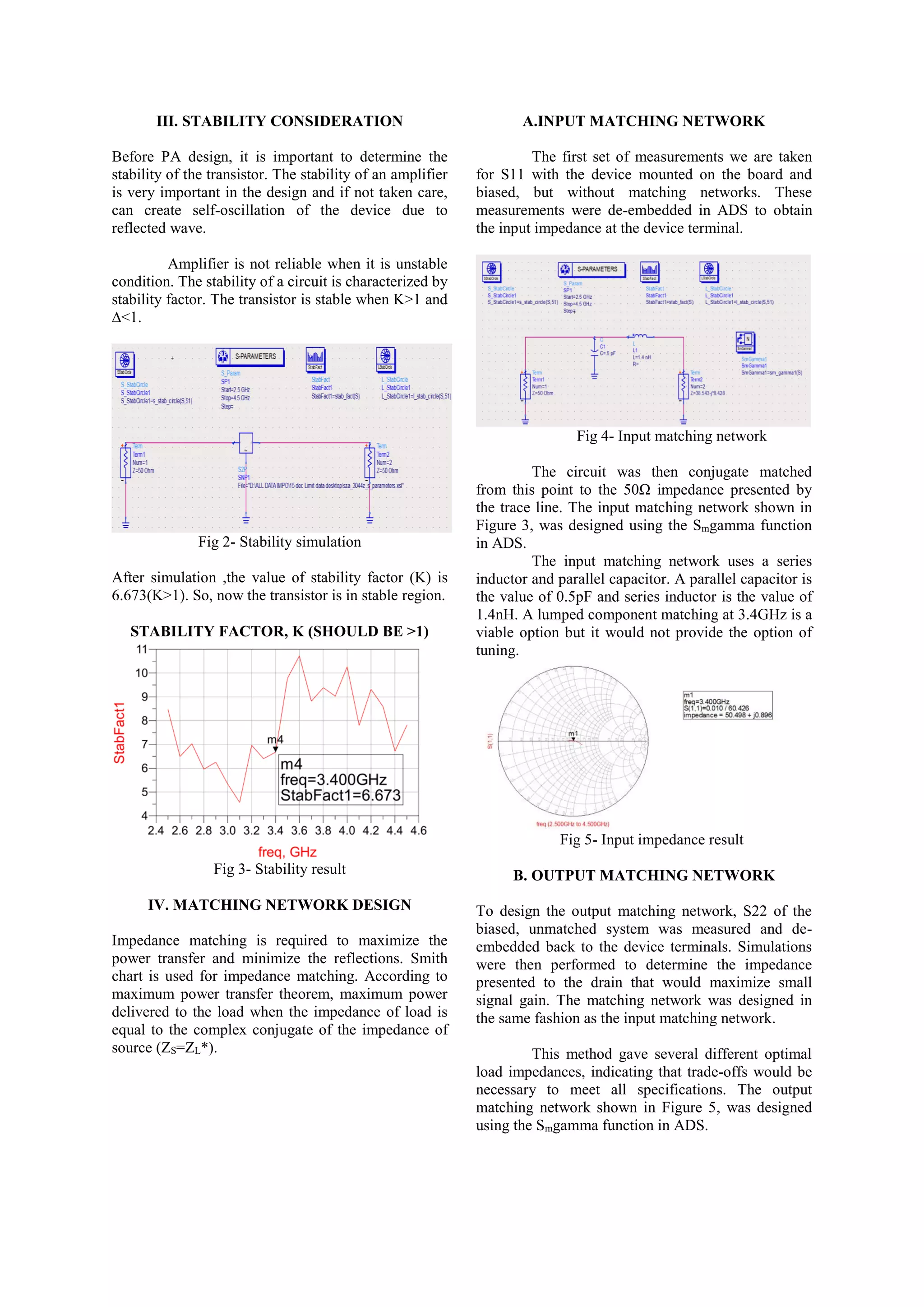
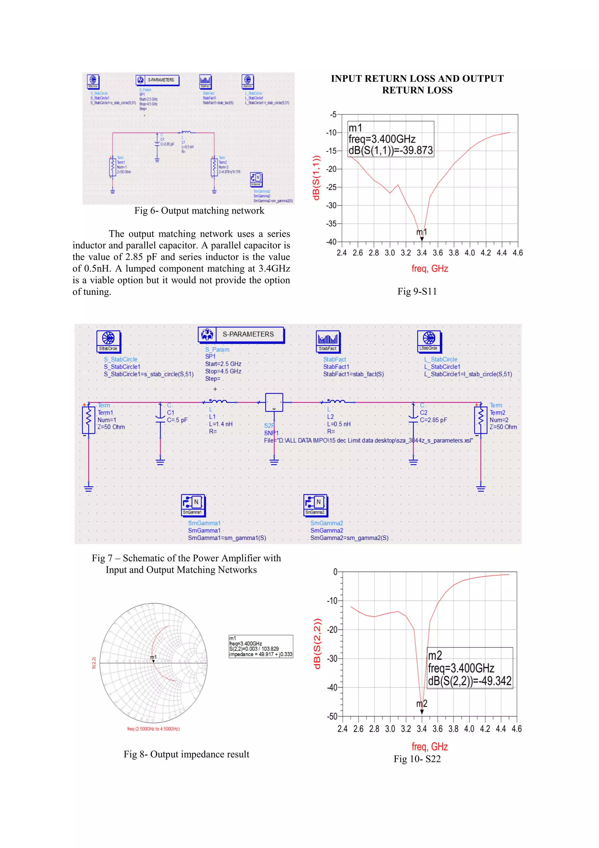
V. MEASURED RESULTS
The complete schematic of the power
amplifier is shown in the Figure 6. The performance
results are shown in the Figs.9,10,11. The S11 is
shown in Figure 9. The region between 2.5 to 4.5GHz
has S11 in the order of -39.873dB, S22 in the order of
-49.342dB from measurements and the S21 gain
value is 26.412dB shown in Figure 11.
TABLE II
MEASURED RESULTS
VI. CONCLUSION
The power amplifier presented here doesn’t meet
many of the required specifications. Still a Stable
Power amplifier with certain loss of power has been
designed with proper matching networks. But
working on this design provided a lot on insight into
design of power amplifiers and the problems faced
when the specifications require designs to be
extremely competitive in terms of performance.
The choice of transistor in this power
amplifier has influenced the design specifications in
an unexpected manner. To make a power amplifier
utilizing this device, a wide variety of matching
networks should be explored along with an
appropriate device modelling in ADS.
VII. ACKNOWLEDGEMENT
The Author thanks Prof.A.K Sisodia & Ast Prof.
Nimesh M. Prabhakar from L.J.Institute of
Engineering and Technology for technical discussion
& processing support without whom this paper would
never be complected.
VIII. REFERENCES
[1] Tomohiro Senju, Takashi Asano, Hiroshi
Ishimura Microwave Solid-state Department “A
VERY SMALL 3.5 GHz 1 W MMIC POWER
AMPLIFIER WITH DIE SIZE REDUCTION
TECHNOLOGIES” Komukai Operations Toshiba
Corporation, Komukai, Toshiba-cho, Saiwai-ku,
Kawasaki 2 12-858 1, Japan-2001 IEEE, pp. 070-073
,ISBN:0-7803-7161-5/01.
[2] Kevin W. Kobayashi, YaoChung Chen, Ioulia
Smorchkova, Roger Tsai,Mike Wojtowicz, and Aaron
Oki “A 2 Watt, Sub-dB Noise Figure GaN MMIC
LNA-PA Amplifier with Multi-octave Bandwidth
from 0.2-8 GHz” 2007 IEEE - SIRENZA
MICRODEVICES, pp.619 -622,ISBN:1-4244-0688-
9/07.
[3] Paul saad, christian fager, hossein mashad nemati,
haiying cao, herbert zirath and kristoffer andersson ”
A highly efficient 3.5 GHz inverse class-F GaN
HEMT power amplifier” European Microwave
Association International Journal of Microwave and
Wireless Technologies, 2010, 2(3-4), pp.317–
332,DOI:10.1017.
[4] Bilkent University, Nanotechnology Research
Center, Bilkent, Ankara, Istanbul Technical
University, Electrical & Electronics Faculty,Maslak,
Istanbul, Turkey ” Design of High Power S-Band
GaN MMIC Power Amplifiers for WiMAX
Applications” 2011 IEEE, pp.01-04,ISBN:978-1-
4244-6051-9/11.
[5] Ahmed Sayed, Georg Boeck Microwave
Engineering, Berlin University of Technology
Einsteinufer 25, 10587 Berlin, Germany ” 5W
Highly Linear GaN Power Amplifier with 3.4 GHz
Bandwidth”European Microwave Integrated Circuits
Conference 2007 EuMA , pp.631 – 634,ISBN:978-2-
87487-002-6.
[6] U. K. Mishra, P. Parikh, and Y.-F. Wu,
“AlGaN/GaN HEMTs−An overview of device
operations and applications”, Proceedings of the
IEEE, vol. 90, no. 6, June 2002, pp. 1022–
1031,ISBN:2230-7109.
Parameter Symbol Specification Measured
results
Gain S21 ≥15dB 26.412dB
Input return
loss
S11 ≤ -10dB -39.873dB
Output return
loss
S22 ≤ -10dB -49.342dB
Input/output
Impedance
Z0 50Ω 50Ω](https://image.slidesharecdn.com/3776e5cf-f299-41e1-8ff8-336cd2b5ac6c-160314104709/75/neelpaper-4-2048.jpg)
![[7] U. K. Mishra, L. Shen, T. E. Kazior, and Y.-F.
Wu, “GaN-Based RF Power Devices and
Amplifiers”, Proceedings of the IEEE, vol. 96, no. 2,
February 2008, pp. 287 – 305,ISBN:2230-9543.
[8] S. Keller et al., “Gallium Nitride Based High
Power Heterojunction Field Effect Transistors:
Process Development and Present Status at UCSB”,
IEEE Transactions on Circuits and Systems, vol. 48,
no. 3, March 2001, pp. 552 – 559,ISBN:2278-0181.
[9] U.Schmid et al., “GaN devices for communication
applications: evolution of amplifier architectures”,
International Journal of Microwave and Wireless
Technologies, Cambridge University Press and the
European Microwave Association, 2010, pp. 85–
93,DOI:10.1088/1674-4926/32/9/094003.
[11] Nemati, H.; Fager, C.; Thorsell, M.; Herbert, Z
“High-efficiency LDMOS power-amplifier design at
1 GHz using an optimized transistor model”. IEEE
Trans. Microw. Theory Tech., 57 (7) (2009), pp.
1647–1654,ISSN:3840-7001.
[12] Rollett, J. “Stability and power-gain invariants of
linear two ports”. IEEE Trans. Circuit Theory, 9 (1)
(2010), pp. 29–32,ISBN:978-1-4673-1088-8/12.
[13] Kim, J.; Konstantinou, K.”Digital predistortion
of wideband signals based on power amplifier model
with memory”. Electron. Lett., 37 (2001), pp. 1417–
1418, ISSN:0-7803-8331-1/04.
[14] Nagy, W.; Brown, J.; Borges, R.; Singhal, S.
“Linearity characteristics of microwave-power GaN
HEM”. IEEE Trans. Microw, 51 (2) (2012), pp.660–
664, ISSN:0018-9480.
[15] U. K. Mishra, L. Shen, T. E. Kazior, and Y.-F.
Wu, “GaN-Based RF Power Devices and
Amplifiers”, Proceedings of the IEEE, vol. 96, no. 2,
February 2009, pp. 287 – 305, ISSN:978-1-4244-
2893-9/09.](https://image.slidesharecdn.com/3776e5cf-f299-41e1-8ff8-336cd2b5ac6c-160314104709/75/neelpaper-5-2048.jpg)


![[IJET-V1I2P6] Authors :Sarat K Kotamraju, K.Ch.Sri Kavya, A.Gnandeep Reddy, G...](https://cdn.slidesharecdn.com/ss_thumbnails/ijet-v1i2p6-150501052009-conversion-gate02-thumbnail.jpg?width=640&height=640&fit=bounds)