Download to read offline
![International Journal of Engineering and Technical Research (IJETR)
ISSN: 2321-0869, Volume-1, Issue-10, December 2013
13 www.erpublication.org
Abstract— in this paper performance of DC drive fed by high
step-up converter is studied. High step up zeta converter is
employed here with solar PV as a source without Extreme duty
ratios and the numerous turns-ratios of a coupled inductor ,
converter achieves a high step-up voltage-conversion ratio and
the leakage inductor energy of the coupled inductor is efficiently
recycled to the load. These features explain the module’s high
efficiency performance. The operating principles and
steady-state analyses of continuous and boundary conduction
modes, as well as the voltage and current stresses of the active
components, are analyzed for a 250W circuit model using
MATLAB SIMULINK.
Index Terms— Zeta converter, PWM technique, Coupled
Inductor, Active Switch.
I. INTRODUCTION
In recent years photovoltaic (PV) has became attractive as
a result PV market would grow up to 30 GW by 2014, due to
the following policy-driven scenario [1];One type of
renewable energy source is the photovoltaic (PV) cell, which
converts sunlight to electrical current, without any form for
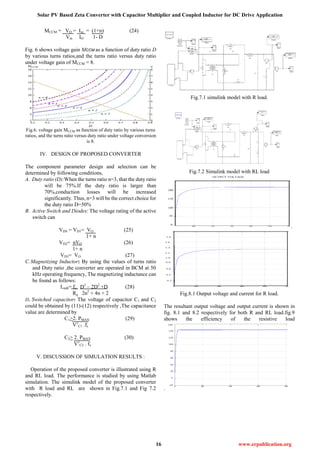
mechanical or thermal interlink. Fig.1 Shows the block
diagram of the proposed converter, that the PV panel
(100~300W) is connected to the high step-up DC_DC
converter, the input voltage of the converter is 15~40Volt
from the PV panel.
Fig.1 General configuration of DC module.
PV cells are usually connected together to make PV modules,
consisting of 72 PV cells, which generates a DC voltage
between 15 Volt to 45 Volt and a typical maximum power of
160 Watt, depending on temperature and solar irradiation.
Fig. 2 shows that the maximum power point (MPP) voltage
Manuscript received November 29, 2013.
G.Arthiraja, PG Scholar, Dept. of Power Electronics and Drives, Jeppiaar
engineering College, Chennai, India, 9677969377.
B. Arunkumaran, PG Scholar, Dept. of Power Electronics and Drives,
Jeppiaar Engineering College, Chennai, India, 9445484322.
M. Ammal Dhanalakshm, PG Scholar, Dept. of Power Electronics and
Drives, Jeppiaar Engineering College, Chennai, India, 9677282451.
M. Sasikumar, Professor & Head, Dept. of Power Electronics and
Drives, Jeppiaar Engineering College, Chennai, India, 9094277053.
range is from 15 V to 40 V with various power capacities of
about 100 W to 300 W for a single commercial PV panel.
Fig.2 MPP voltage (Vmp) distribution with various power
capacities of PVpanel.
The typical Zeta converter will provide either a step-up or a
step-down function to the output, similar to that of the
buck-boost or SEPIC converter topologies.The conventional
Zeta converter has been configured of two inductors, a series
capacitor and a diode. Previous research works have
developed diverse Zeta converter applications, as follows.A
coupled inductor could be employed to reduce power supply
dimensions[2]. Some Zeta and fly back combination
converters have extend the output range by the use of this
coupled-inductor technique[3],[5]. ]. By Employing soft
switching technique, zero-voltage switching and zero-current
switching, on the Zeta converter; and hanging the input
inductor of the ZETA converter[3],[6],[7]; to a coupled
inductor have obtained a higher step-up conversion
ratio[8],[20]. Many research works on high step-up converter
topology included analyses of the switched-inductor and
switched-capacitor types[9]–[11],transformerless
switched-capacitor type [12], [13],the boost type integrated
with the coupled inductor [14], [15], the voltage-lift type and
the capacitor-diode voltage multiplier. The equivalent series
resistance (ESR) of the capacitor and the parasitic resistances
of the inductor are also affecting the overall efficiency. In
regard to increasing voltage gain, this attribute is constricted
by the voltage stress on the active switch. However, if the
leakage inductor energy of the coupled inductor could be
recycled, then the voltage stress is reduced on the active
switch, that means the coupled-inductor and the
voltage-multiplier or voltage-lift techniques are able to
accomplish the goal of achieving higher voltage gain
[2]–[22].The DC-DC boost converter is used for voltage
step-up applications, and in this case this converter will be
Solar PV Based Zeta Converter with Capacitor
Multiplier and Coupled Inductor for DC Drive
Application
G.Arthiraja, M. Ammal Dhanalakshmi, B.Arunkumaran and M. Sasikumar](https://image.slidesharecdn.com/ijetr012011-171119123826/85/Ijetr012011-1-320.jpg)
![International Journal of Engineering and Technical Research (IJETR)
ISSN: 2321-0869, Volume-1, Issue-10, December 2013
13 www.erpublication.org
Abstract— in this paper performance of DC drive fed by high
step-up converter is studied. High step up zeta converter is
employed here with solar PV as a source without Extreme duty
ratios and the numerous turns-ratios of a coupled inductor ,
converter achieves a high step-up voltage-conversion ratio and
the leakage inductor energy of the coupled inductor is efficiently
recycled to the load. These features explain the module’s high
efficiency performance. The operating principles and
steady-state analyses of continuous and boundary conduction
modes, as well as the voltage and current stresses of the active
components, are analyzed for a 250W circuit model using
MATLAB SIMULINK.
Index Terms— Zeta converter, PWM technique, Coupled
Inductor, Active Switch.
I. INTRODUCTION
In recent years photovoltaic (PV) has became attractive as
a result PV market would grow up to 30 GW by 2014, due to
the following policy-driven scenario [1];One type of
renewable energy source is the photovoltaic (PV) cell, which
converts sunlight to electrical current, without any form for
mechanical or thermal interlink. Fig.1 Shows the block
diagram of the proposed converter, that the PV panel
(100~300W) is connected to the high step-up DC_DC
converter, the input voltage of the converter is 15~40Volt
from the PV panel.
Fig.1 General configuration of DC module.
PV cells are usually connected together to make PV modules,
consisting of 72 PV cells, which generates a DC voltage
between 15 Volt to 45 Volt and a typical maximum power of
160 Watt, depending on temperature and solar irradiation.
Fig. 2 shows that the maximum power point (MPP) voltage
Manuscript received November 29, 2013.
G.Arthiraja, PG Scholar, Dept. of Power Electronics and Drives, Jeppiaar
engineering College, Chennai, India, 9677969377.
B. Arunkumaran, PG Scholar, Dept. of Power Electronics and Drives,
Jeppiaar Engineering College, Chennai, India, 9445484322.
M. Ammal Dhanalakshm, PG Scholar, Dept. of Power Electronics and
Drives, Jeppiaar Engineering College, Chennai, India, 9677282451.
M. Sasikumar, Professor & Head, Dept. of Power Electronics and
Drives, Jeppiaar Engineering College, Chennai, India, 9094277053.
range is from 15 V to 40 V with various power capacities of
about 100 W to 300 W for a single commercial PV panel.
Fig.2 MPP voltage (Vmp) distribution with various power
capacities of PVpanel.
The typical Zeta converter will provide either a step-up or a
step-down function to the output, similar to that of the
buck-boost or SEPIC converter topologies.The conventional
Zeta converter has been configured of two inductors, a series
capacitor and a diode. Previous research works have
developed diverse Zeta converter applications, as follows.A
coupled inductor could be employed to reduce power supply
dimensions[2]. Some Zeta and fly back combination
converters have extend the output range by the use of this
coupled-inductor technique[3],[5]. ]. By Employing soft
switching technique, zero-voltage switching and zero-current
switching, on the Zeta converter; and hanging the input
inductor of the ZETA converter[3],[6],[7]; to a coupled
inductor have obtained a higher step-up conversion
ratio[8],[20]. Many research works on high step-up converter
topology included analyses of the switched-inductor and
switched-capacitor types[9]–[11],transformerless
switched-capacitor type [12], [13],the boost type integrated
with the coupled inductor [14], [15], the voltage-lift type and
the capacitor-diode voltage multiplier. The equivalent series
resistance (ESR) of the capacitor and the parasitic resistances
of the inductor are also affecting the overall efficiency. In
regard to increasing voltage gain, this attribute is constricted
by the voltage stress on the active switch. However, if the
leakage inductor energy of the coupled inductor could be
recycled, then the voltage stress is reduced on the active
switch, that means the coupled-inductor and the
voltage-multiplier or voltage-lift techniques are able to
accomplish the goal of achieving higher voltage gain
[2]–[22].The DC-DC boost converter is used for voltage
step-up applications, and in this case this converter will be
Solar PV Based Zeta Converter with Capacitor
Multiplier and Coupled Inductor for DC Drive
Application
G.Arthiraja, M. Ammal Dhanalakshmi, B.Arunkumaran and M. Sasikumar](https://image.slidesharecdn.com/ijetr012011-171119123826/75/Ijetr012011-1-2048.jpg)
![Solar PV Based Zeta Converter with Capacitor Multiplier and Coupled Inductor for DC Drive Application
14 www.erpublication.org
operated at extremely high duty ratio to achieve high step-up
voltage gain. However, the voltage gain and the efficiency are
limited due to the constraining effect of power switches,
diodes, and the equivalent series resistance (ESR) of
inductors and capacitors. Moreover, the extremely high
duty-ratio operation will result in a serious reverse-recovery
problem. Much higher voltage gain is achieved by using the
coupled inductor and the voltage-multiplier or voltage-lift
techniques. The operating principles and steady-state analysis
are presented in the following sections.
II. OPERATING PRINCIPLES OF THE
PROPOSED CONVERTERS
Fig. 3 shows the circuit configuration of the proposed
converter, which consists of two active switch S1,one coupled
inductor, three diodes D1~D3 and three capacitor C1~C3.The
coupled inductor is modeled as a magnetizing inductor L
m
,
primary leakage inductor L
k1
, secondary leakage inductor L
k2
,
and an ideal transformer.
Fig.3 simplified model of proposed converter.
All components are ideal. The ON-state resistance RDS(ON)
of the active switches, the forward voltage drop of the diodes,
and the equivalent series resistance (ESR) of the
coupled-inductor and output capacitors are ignored The turns
ratio n of the coupled inductor T1 winding is equal to
N2/N1.Fig. 4 shows some typical waveforms during one
switching period in continuous conduction mode (CCM)
operation. The operating principle and the five operating
modes are described as follows.
A. CCM Operation
Mode I [t0,t1]: In this interval the capacitor C2 obtain energy
continuously from the secondary leakage inductor Lk2.The
current flow path is shown in Fig. 5(a); switch S1 and diodes
D2 are conducting. The source voltage Vin is applied on
magnetizing inductor Lm and primary leakage inductor Lk1
,the current iLm is decreased; at the same time, Lm also releases
its energy to the secondary winding, as well as charges the
capacitor C2 along with the decrease in energy, the charging
current iD2 and iC2 also decreases. The secondary leakage
inductor current iLK2 is being declined according to iLm/n. Once
when the increasing iLk1 equals the decreasing iLm this mode
ends at t=t1.
iin(t) = iDS(t) = iLk1(t) (1)
diLm(t) = vLm (2)
dt Lm
diLk1(t) = Vin - vLm (3)
dt Lk1
iLk2(t) = iLm(t) - iLk1(t) (4)
n
Fig.4. Typical waveforms of the proposed converter at CCM
operation.
Mode II [t1, t2]: During this interval, source energy Vinis
connected in series with C1, C2, secondary winding N2, and Lk2
to charge output capacitor C3 and load R; at the same time,
magnetizing inductor Lm also receives energy from Vin. The
path of current flow is shown in Fig. 5(b); as illustrated,
switch S1remains on, and only diode D3 is in conduction. The
iLm, iLk1, and iD3 have been increasing because the Vin
is crossing Lk1, Lm and primary winding N1; Lm and Lk1 are
storing energy from Vin; as well as, Vinis also in series with N2
of coupled inductor T1, and capacitors C1 and C2 have been
discharging their energy to capacitor C3 and load R, that leads
to increases in iLm, iLk1, iDS, and iD3. This mode ends at t = t2 at
which switch S1 is turned off.
iLm(t) = iLk1(t) - niLk2(t) (5)
diLm(t) = Vin (6)
dt Lm
iin(t) = iDS(t) = iLm(t) + (1+n) iLk2(t) (7)
diLk2(t) = diD3(t) = (1+n)Vin + VC1 + VC2 (8)
dt dt Lk2
Mode III [t2, t3]:During this transition interval, C3 is being
charged from secondary leakage inductor Lk2 when switch S1
is turned off. The current flow path is shown in Fig. 5(c), and
the diodes D1 and D3 are conducting. The energy stored in
leakage inductor Lk1 is flowing through diode D1 and the
capacitor C1 is charged instantly when S1 turns off. Also, the
Lk2 keeps the same current direction as in the previous mode
and is in series with C2 to charge output capacitor C3 and load
R. The summation of Vin, VLm, and VLk1 is the voltage across S1.
Currents iLk1 and iLk2 are rapidly declining, but iLm increases
because Lmis receiving energy from Lk2. Once when the
current iLk2 drops to zero, this mode endsatt= t3.
iin(t) = 0 (9)](https://image.slidesharecdn.com/ijetr012011-171119123826/85/Ijetr012011-2-320.jpg)
![International Journal of Engineering and Technical Research (IJETR)
ISSN: 2321-0869, Volume-1, Issue-10, December 2013
15 www.erpublication.org
iLm(t) = iLk1(t) - niLk2(t) (10)
diLk1(t) = -VC1 – vLm (11)
dt Lk1
diLk2(t) = diD3(t) = n vLm + VC1 – Vo (12)
dt dt Lk2
(a)
(b)
(c)
(d)
(e)Fig.5. During CCM operation, current flowing path in five
modes operation (a) Mode I. (b) Mode II. (c) Mode III. (d)
Mode IV. (e) Mode V.
Mode IV [t3, t4]:In this transition interval, the energy stored in
magnetizing inductor Lm is released simultaneously to C1 and
C2. The current flow path is shown in Fig. 5(d). and the
diodes D1 and D2 are conducting. As leakage energy still
flows through diode D1 and continues to charge capacitor
C1,Currents iLk1 and iD1 are persistently being decreased.
Through T1 and D2 , the Lmis delivering its energy for charging
capacitor C2. The energy stored in capacitors C3 is discharged
constantly to the load R. The voltage across S1 is the same as
in the prior mode. Current iD2 is increasing but iLk1 and iLm are
decreasing, but. This mode ends when current iLk1 becomes
zero at t = t4.
iLm(t) = iLk1(t) - niLk2(t) (13)
diLk1(t) = -VC1 – vLm (14)
dt Lk1
diLk2(t) = n vLm + VC2 (15)
dt Lk2
Mode V [t4, t5]:In this interval, magnetizing inductor Lm
constantly transfers energy to C2. The current flow path is
shown in Fig. 5(e), and diode D2 is alone conducting. Due to
the continuous flow of magnetizing inductor energy through
the coupled inductor T1 to secondary winding N2 and D2 for
charging capacitor C2 the iLm is decreasing. The stored energy
in capacitors C3 constantly discharges to the load R. The
summation of Vin and VLm is the voltage across S1.When switch
S1 is turned on at the beginning of the next switching period
this mode ends.
diLm(t) = vLm (16)
dt Lm
iLk1(t) = 0 (17)
diLk2(t) = n vLm + VC2 (18)
dt Lk2
III. STEADY-STATE ANALYSIS OF PROPOSED
CONVERTERS
CCM Operation:
To simplify the steady-state analysis, only modes II and IV
are considered for CCM operation, and the primary &
secondary side of leakage inductance are ignored. During
mode II the following equations can be written,
vLm= Vin
vN2 = nVin
The following equations can be written from mode IV:
vLm = -Vc1
-vN2 = Vc2.
Applying a volt-second balance on the magnetizing inductor
Lm yields
ʃ DTS
(Vin)dt + ʃ DTS
(-VC1)dt = 0 (19)
0 0
ʃ DTS
(nVin)dt + ʃ DTS
(-VC2)dt = 0 (20)
0 0
the voltage across capacitor C1 and C2 are
VC1 = D Vin (21)
1- D
VC2 = n DVin (22)
1- D
The output voltage Vo and the voltage gain MCCM can be
written as
VO = Vin + DVin+ nVin+ nD Vin = (1+n)Vin (23)
1- D 1- D 1- D](https://image.slidesharecdn.com/ijetr012011-171119123826/85/Ijetr012011-3-320.jpg)
![International Journal of Engineering and Technical Research (IJETR)
ISSN: 2321-0869, Volume-1, Issue-10, December 2013
17 www.erpublication.org
Fig.8.2 output voltage and current for RL load.
Fig.9 Efficiency versus resistive load.
VI. CONCLUSION
A high efficient DC/DC boost converter is proposed in this
paper. The efficiency of the converter is improved by utilizing
the energy stored in the coupled inductor and the two
capacitors. Thus it makes the boost converter to implement in
the drive applications. The experimental results prove that
high voltage gain and efficiency are achieved. The results
show that applying coupled-inductor turns ratio of n = 3 to the
eight-times step-up voltage-conversion ratio attains maximum
efficiency.
REFERENCES
[1] Global Market Outlook for Photovoltaics Until 2014, Eur.
PhotovoltaicInd. Assoc. (EPIA), Brussels, Belgium, May 2010. [Online].
Available:http://www.epia.org/fileadmin/EPIA_docs/public/Global_Market
_Outlook_for_Photovoltaics_until_2014.pdf
[2] J. Falin, ―Designing dc/dc converters based on ZETA topology,‖Analog
Appl. J., pp. 16–21, 2Q, 2010. [Online]. Available:
http://focus.ti.com/lit/an/slyt372/slyt372.pdf
[3] B. R. Lin and F. Y. Hsieh, ―Soft-switching Zeta-flyback converter witha
buck-boost type of active clamp,‖ IEEE Trans. Ind. Electron., vol. 54,no. 5,
pp. 2813–2822, Oct. 2007.
[4] T. B. Marchesan, M. A. Dalla-Costa, J. M. Alonso, and R. N. do
Prado,―Integrated Zeta-flyback electronic ballast to supply high-intensity
dischargelamps,‖ IEEE Trans. Ind. Electron., vol. 54, no. 5, pp.
2918–2921,Oct. 2007.
[5] D. Murthy-Bellur and M. K. Kazimierczuk, ―Two-transistor
Zeta-flybackdc-dc converter with reduced transistor voltage stress,‖
Electron. Lett.,vol. 46, no. 10, pp. 719–720, May 2010
[6] T. F. Wu, S. A. Liang, and Y. M. Chen, ―Design optimization for
asymmetricalZVS-PWM Zeta converter,‖ IEEE Trans. Aerosp.Electron.
Syst.,vol. 39, no. 2, pp. 521–532, Apr. 2003.
[7] R.Sudha,Ms.Ashly Mary Tom and M.Sasikumar (2012), ‗An Efficient
Non Isolated ZVT Boost Converter With A Single Resonant Inductor for
Drive Applications,‘ International Journal of Knowledge Engineering and
Research, Vol.1, Issue 2 , Pp. 76-80.
[8] B. Axelrod, Y. Berkovich, S. Tapuchi, and A. Ioinovici, ―Steep
conversionration C´ uk, Zeta, and sepic converters based on a
switchedcoupled-inductor cell,‖ in Proc. IEEE Power Electron. Spec. Conf.,
2008,pp. 3009–3014.
[9] B.Axelrod, Y.Berkovich,and A.Ioinovici,―Switched-capacitor/switched-
inductor structures for getting transformerless hybrid dc-dc PWM
converters,‖ IEEE Trans. Circuits Syst. I, Reg. Papers, vol. 55, no. 2,pp.
687–696, Mar. 2008.
[10] F. L. Luo, ―Switched-capacitorized dc/dc converters,‖ in Proc.
IEEEICIEA, 2009, pp. 1074–1079.
[11] B. Axelrod, Y. Berkovich, and A. Ioinovici, ―Transformerless dc-dc
converterswith a very high dc line-to-load voltage ratio,‖ in Proc.
IEEEISCAS, 2003, vol. 3, pp. 435–438.
[12] L. S. Yang, T. J. Liang, and J. F. Chen, ―Transformerless dc-dc
converterswith high step-up voltage gain,‖ IEEE Trans. Ind. Electron., vol.
56, no. 8,pp. 3144–3152, Aug. 2009.
[13] Q. Zhao and F. C. Lee, ―High-efficiency, high step-up dc-dc
converters,‖IEEE Trans. Power Electron., vol. 18, no. 1, pp. 65–73, Jan.
2003.
[14] L. S. Yang, T. J. Liang, H. C. Lee, and J. F. Chen, ―Novel highstep-up
dc-dc converter with coupled-inductor and voltage-doubler circuits,‖IEEE
Trans. Ind. Electron., vol. 58, no. 9, pp. 4196–4206,Sep. 2011.
[15] H.-L. Do, ―Zero-voltage-switching synchronous buck converter with
acoupled inductor,‖ IEEE Trans. Ind. Electron., vol. 58, no. 8, pp.
3440–3447, Aug. 2011.
[16]G.S Arunvishnu, S.Sellakumar and M.Sasikumar (2012),‗Simulation
and implementation of Variable Duty Cycle Control to Achieve High Input
Power Factor for DCM Boost PFC Converters‖ International Journal of
Engineering Research and Applications (IJERA), Vol. 2, Issue 2,
Pp.138-141.
[17].F. Max Savio, R. Hemantha Kumar and M. Sasikumar (2013), ―Power
Optimisation and Performance Evolution of High Step-Up Solar PV System
For Dc Drives‖, International Journal of Advanced Research in Electrical,
Electronics and Instrumentation Engineering (IJAREEIE),Vol. 2, Issue 10,
October 2013.
G. Arthiraja is currently pursuing Master of Engineering
in Power Electronics and Drives in Jeppiaar Engineering
College, Anna University, Chennai, Tamilnadu. Earlier he
received his B.E degree in Electrical and electronics
Engineering in Sri Sairam Engineering college, Anna
University, Chennai in 2012. His current research interests
include Renewable Energy Sources and DC-DC
Converters.
M. Ammal Dhanalakshmi is currently pursuing Master of
Engineering in Power Electronics and Drives in Jeppiaar
Engineering College, Anna University, Chennai,
Tamilnadu. Earlier she received her B.E degree in
Elecrtrical and Electronics Engineering in Vel‘s Srinivasa
college of engineering and technology, Chennai in 2009.
Her current research interests include soft switching
DC-DC Converters. She is a life member of ISTE.
B. ArunKumaran is currently pursuing Master of
Engineering in Power Electronics and Drives in Jeppiaar
Engineering College, Anna University, Chennai,
Tamilnadu. Earlier he received his B.E degree in
Electronics and Instrumentation Engineering in
Thangavelu Engineering college, Anna University,
Chennai in 2011. His current research interests includes
Renewable Energy Sources and DC-DC Converters.
Dr.M.Sasikumar has received the Bachelor degree in
Electrical and Electronics Engineering from
K.S.Rangasamy College of Technology, Madras
University, India in 1999, and the M.Tech degree in
power electronics from VIT University, in 2006. He has
obtained his Ph.d. degree from Sathyabama University,
Chennai. Currently he is working as a Professor and
Head in Jeppiaar Engineering College, Chennai
Tamilnadu, India. He has published papers in National, International
conferences and journals in the field of power electronics and wind energy
conversion systems. His area of interest includes in the fields of wind energy
systems and power converter with soft switching PWM schemes. He is a life
member of ISTE.](https://image.slidesharecdn.com/ijetr012011-171119123826/85/Ijetr012011-5-320.jpg)

The document summarizes a study on using a high step-up zeta converter fed by a solar PV panel for a DC drive application. Key points: - A zeta converter with a coupled inductor and capacitor multiplier is used to achieve high step-up voltage conversion from a 15-40V solar PV panel input. - Steady-state analysis of the converter in continuous conduction mode shows it can achieve a voltage gain of (1+n) where n is the turns ratio of the coupled inductor. - Simulation results using Matlab/Simulink validate the converter design and show it can provide the required output voltage for a DC drive from the solar PV input with high efficiency for resist


![[IJET V2I5P9] Authors: Anju John Gray, Beena M Vargheese, Miss. Geethu James](https://cdn.slidesharecdn.com/ss_thumbnails/ijet-v2i5p9-161107141042-thumbnail.jpg?width=640&height=640&fit=bounds)


![[IJET V2I5P8] Authors: Lakshmi K R, Kavitha Issac, Kiran Boby](https://cdn.slidesharecdn.com/ss_thumbnails/ijet-v2i5p8-161107140749-thumbnail.jpg?width=640&height=640&fit=bounds)


