Downloaded 16 times

![G. Shiny Vikram Int. Journal of Engineering Research and Applications www.ijera.com
ISSN : 2248-9622, Vol. 4, Issue 9( Version 1), September 2014, pp.160-164
www.ijera.com 161 | P a g e
reverse direction, only little reverse saturation current
could get through. All the equations for modeling the
PV array are analyzed based on this equivalent circuit
Fig 2.1 Mat lab model of single pv-cell
III. Coupled inductor Boost converter
Bidirectional dc–dc converters are used to
transfer the power between two dc sources in either
direction. These converters are widely used in
applications, such as hybrid electric vehicle energy
systems, uninterrupted power supplies, fuel-cell
hybrid power systems photovoltaic hybrid power
systems and battery chargers .Many bidirectional dc–
dc converters have been researched. The bidirectional
dc–dc fly back converters are more attractive due to
simple structure and easy control However; these
converters suffer from high voltage stresses on the
power devices due to the leakage inductor energy of
the transformer. In order to recycle the leakage
inductor energy and to minimize the voltage stress on
the power devices, some literatures present the
energy regeneration techniques to clamp the voltage
stress on the power devices and to recycle the leakage
inductor energy .Some literatures research the
isolated bidirectional dc–dc converters, which
include the half-bridge and full-bridge types .These
converters can provide high step-up and step-down
voltage gain by adjusting the turns ratio of the
transformer. The multilevel type is a magnetic less
converter, but 12 switches are used in this converter.
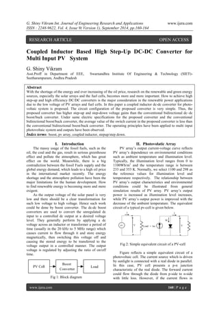
Fig 3: Proposed boost converter
A modified dc–dc boost converter is presented
the voltage gain of this converter is higher than the
conventional dc–dc boost converter. Based on this
converter, a novel bidirectional dc–dc converter is
proposed, as shown in Fig. 2. The proposed converter
employs a coupled inductor with same winding turns
in the primary and secondary sides. Comparing to the
proposed converter and the conventional bidirectional
boost/buck converter, the proposed converter has the
following advantages: 1) Higher step-up and step-down
voltage gains and 2) lower average value of the
switch current under same electric specifications. The
following sections will describe the operating
principles and steady-state analysis for the step-up
and step-down modes. In order to analyze the steady-state
characteristics of the proposed converter, some
conditions are assumed: The ON-state resistance RDS
(ON) of the switches and the equivalent series
resistances of the coupled inductor and capacitors are
ignored; the capacitor is sufficiently large; and the
voltages across the capacitor can be treated as
constant.
3.1 .Step-Up Mode
The proposed converter can be used for both
step up and step down modes with suitable
switching of the devices. The proposed converter in
step-up mode is shown in Fig. 3. Since the primary
and secondary winding turns of the coupled inductor
is same, the inductance of the coupled inductor in the
primary and secondary sides are expressed as
L1 = L2 = L. (1)
Thus, the mutual inductance M of the coupled
inductor is given by
M = k 퐿1 퐿2= KL (2)
Where k is the coupling coefficient
of the coupled inductor. The voltages across the
primary and secondary windings of the coupled
inductor are as follows:
Since the proposed converter can be used for
both continuous (CCM) and discontinuous
conduction (DCM) only the continuous conduction
mode (CCM) is preferred for the analysis for best
understanding of the operation.
3.2 CCM operation
Mode 1: During this time interval [t0, t1], S1 and S2
are turned on and S3 is turned off. The current flow
path is shown in Fig. 3(a). The energy of the low-](https://image.slidesharecdn.com/x4901160164-141021015253-conversion-gate01/85/Coupled-Inductor-Based-High-Step-Up-DC-DC-Converter-for-Multi-Input-PV-System-2-320.jpg)
![G. Shiny Vikram Int. Journal of Engineering Research and Applications www.ijera.com
ISSN : 2248-9622, Vol. 4, Issue 9( Version 1), September 2014, pp.160-164
www.ijera.com 163 | P a g e
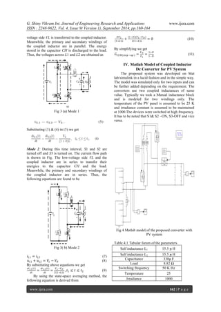
V. Simulation results
The performance of the proposed converter was verified using mat lab/simulink. Some experimental results in step-up are shown in Fig 5, shows the waveforms of the total input current iL and the coupled inductor currents iL1 and iL2 in step-up mode. It can be observed that iL1 is equal to iL2.
Fig 5(a) Combined Input to the dc converter form pv panels.Vin = 32 V
Fig 5(b) Output voltage from the dc converter VOUT = 96.7V
Fig 5(c) Equal Current through switching devices S1 & S2
Fig 5 (d) Equal currents through coupling inductors (L1 & L2)
Fig 5(e).Total input current
VI. Conclusion
The proposed dc converter is simple in construction and has more efficiency than the conventional dc-dc converter. This can be used in battery operated vehicles, and solar powered uninterrupted power supplies and can have significant use in renewable energy sources where there is a need of efficient dc conversion. References [1]. Novel high step up dc to dc converter with coupled inductor and switched capacitor for a sustainable energy system by Lung-Sheng Yang and Tsorng-Juu Liang, -IEEE TRANSACTIONS ON INDUSTRIAL ELECTRONICS, VOL. 59, NO. 1, JANUARY 2012 [2]. Simulation of Closed Loop Controlled Boost Converter for Solar Installation by Athimulam Kalirasu, Subharensu Sekar Dash-SERBIAN JOURNAL OF ELECTRICAL ENGINEERING Vol. 7, No. 1, May 2010, 121-130 [3]. Simulation of Grid-Connected Photovoltaic System by Jingzhe Song](https://image.slidesharecdn.com/x4901160164-141021015253-conversion-gate01/85/Coupled-Inductor-Based-High-Step-Up-DC-DC-Converter-for-Multi-Input-PV-System-4-320.jpg)
![G. Shiny Vikram Int. Journal of Engineering Research and Applications www.ijera.com
ISSN : 2248-9622, Vol. 4, Issue 9( Version 1), September 2014, pp.160-164
www.ijera.com 164 | P a g e
[4]. Design and Simulation by Photovoltaic System with Tapped Topology by - Juan C. Yris, Hugo Calleja G, Leobardo H. Gonzalez, José A. Olmos -International Journal of Modern Engineering Research (IJMER) Vol.3, Issue.2, March-April. 2013 pp-1238-1244. [5]. A New High Efficient Bi-Directional Dc/Dc Converter In The Dual Voltage System-Su- Won Lee†, Seong-Ryong Lee* and Chil- Hwan Jeon*-Journal of Electrical Engineering & Technology, Vol. 1, No. 3, pp. 343~350, 2006 [6]. High Voltage Gain Boost Converter for Micro source Power Conversion system by K. Radhalakshmi1, R. Dhanasekaran2- ACEEE Int. J. on Electrical and Power Engineering, Vol. 4, No. 1, Feb 20137. M. B. Camara, H. Gualous, F. Gustin, A. Berthon, and B. Dakyo, ―DC/DC converter design for supercapacitor and battery power management in hybrid vehicle applications—Polynomial control strategy,‖ IEEE Trans. Ind. Electron., vol. 57, no. 2, pp. 587–597, Feb. 2010. [7]. L. S. Yang, T. J. Liang, and J. F. Chen, ―Transformerless dc–dc converters with high step-up voltage gain,” IEEE Trans. Ind. Electron., vol. 56, no. 8, pp. 3144– 3152, Aug. 2009. [8]. R. J. Wai and R. Y. Duan, ―High-efficiency bidirectional converter for power sources with great voltage diversity,” IEEE Trans. Power Electron., vol. 22, no. 5, pp. 1986– 1996, Sep. 2007. [9] G. Ma, W. Qu, G. Yu, Y. Liu, N. Liang, and W. Li, ―A zero-voltage switching bidirectional dc–dc converter with state analysis and soft switching- oriented design consideration,‖ IEEE Trans. Ind. Electron., vol. 56, no. 6, pp. 2174–2184, Jun. 2009.
G.Shinyvikram was born in year 1985.He received B.Tech and M.Tech during the years 2007 &2009 respectively both in the field of Electrical Enginering.Presently he is working as Assistant Professor & HOD in Swarnandhra Institute Of Engineering & Technology (SIET) ,Seetharampuram-AndhraPradesh.His area of interests includes control strategies in DC converters, power quality issues, stability analysis of power systems etc.,](https://image.slidesharecdn.com/x4901160164-141021015253-conversion-gate01/85/Coupled-Inductor-Based-High-Step-Up-DC-DC-Converter-for-Multi-Input-PV-System-5-320.jpg)

The document presents a coupled inductor-based high step-up DC-DC converter designed for multi-input photovoltaic systems, emphasizing its simplicity and efficiency compared to conventional converters. It highlights the converter's ability to boost low voltage from solar panels to higher voltage outputs, addressing the challenges posed by energy shortages and high oil prices. Simulation results indicate that the proposed converter exhibits higher voltage gain and lower switch current, making it suitable for applications in renewable energy sources and energy storage systems.


![[IJET V2I5P9] Authors: Anju John Gray, Beena M Vargheese, Miss. Geethu James](https://cdn.slidesharecdn.com/ss_thumbnails/ijet-v2i5p9-161107141042-thumbnail.jpg?width=640&height=640&fit=bounds)


