Download as PDF, PPTX
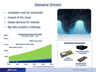
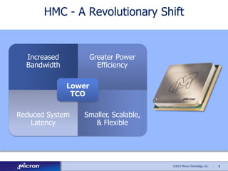
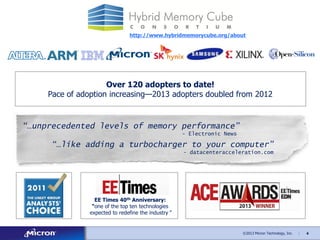
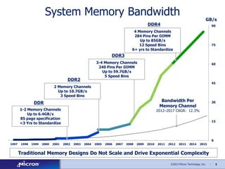
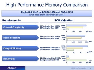
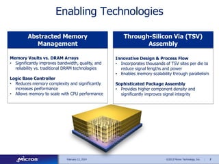
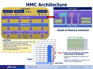
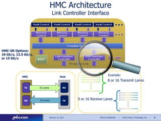
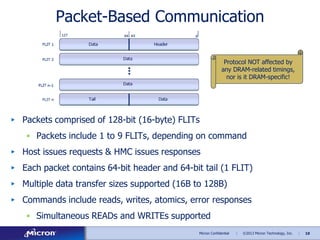

The document discusses the development and advantages of Hybrid Memory Cube (HMC) technology, highlighting its ability to provide unprecedented performance, lower total cost of ownership, and enhanced energy efficiency compared to traditional memory systems. With increasing bandwidth demands driven by trends such as cloud computing and big data, HMC offers a scalable and resilient solution for next-generation data centers. It explains the architectural advancements and key technologies that enable HMC to outperform existing memory solutions, positioning it as a transformative innovation in the memory market.