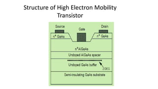
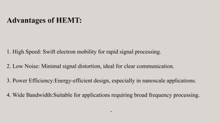
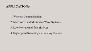
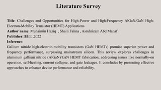
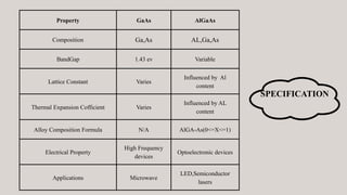
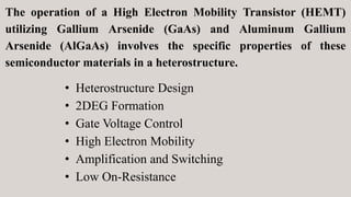
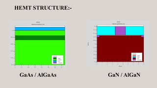
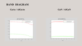
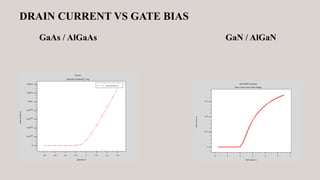
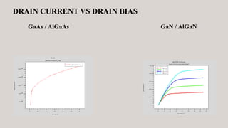
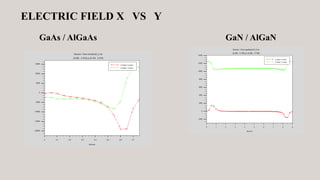
HIGH ELECTRON MOBILITY TRANSISTOR FOR
POWER DEVICE APPLICATION
Mentor:
Dr.T.S.Arun Samuel
Presented by:
Vaishnavi M-2011071
Jenifer D-201092
Selva Archana A-2011110
Problem
statement:-
•Optimization of Device Geometry for High-Frequency Performance
•Investigation of Material Properties and Heterostructure Effects
Objective:
-
1. Optimize GaAs/AlGaAs HEMT geometric parameters for high frequency.
2. Investigate material impact and heterostructure design to enhance cutoff
and oscillation frequencies in comprehensive simulations.
High Electron Mobility
Transistor
1. HEMTs excel in high-frequency tasks with swift electron movement.
2. Ideal for clear signal amplification with minimal noise in communication.
3. Compact design and energy efficiency make HEMTs suitable for advanced
applications.
4. High-speed, low-noise HEMTs contribute to efficient, small-scale electronic
devices..
Structure of High Electron Mobility
Transistor
Advantages of HEMT:
1. High Speed: Swift electron mobility for rapid signal processing.
2. Low Noise: Minimal signal distortion, ideal for clear communication.
3. Power Efficiency:Energy-efficient design, especially in nanoscale applications.
4. Wide Bandwidth:Suitable for applications requiring broad frequency processing.
.
1. Complex Fabrication: Involves intricate processes, leading to higher production
costs.
2. Operating Sensitivity: Some designs may be sensitive to variations, affecting
performance.
3. Temperature Impact: Performance influenced by temperature changes.
4. Voltage Handling Limitations: May have restrictions in voltage handling capabilities
for specific applications.
Dis advantages of HEMT
APPLICATION:-
1. Wireless Communication
2. Microwave and Millimeter-Wave Systems
3. Low-Noise Amplifiers (LNAs)
4. High-Speed Switching and Analog Circuits
Title: Challenges and Opportunities for High-Power and High-Frequency AlGaN/GaN High-
Electron-Mobility Transistor (HEMT) Applications
Author name: Muhaimin Haziq , Shaili Falina , Asrulnizam Abd Manaf
Publisher:IEEE ,2022
Inference:
Gallium nitride high-electron-mobility transistors (GaN HEMTs) promise superior power and
frequency performance, surpassing mainstream silicon. This review explores challenges in
aluminum gallium nitride (AlGaN)/GaN HEMT fabrication, addressing issues like normally-on
operation, self-heating, current collapse, and gate leakages. It concludes by presenting effective
approaches to enhance device performance and reliability.
Literature Survey
Title: GaN Power Integration for High Frequency and High Efficiency Power Applications
Author name: Ruize Sun, Jingxue Lai, Wanjun Chen, Bo Zhang,
Publisher:IEEE ,2020
Inference:
High-frequency and high-efficiency operation are paramount in signal and energy conversion.
Wide bandgap GaN devices outperform Si or GaAs counterparts. This paper advocates for
monolithic power integration in GaN electronics. It explores GaN power device structure,
favoring lateral integration for GaN power ICs. The review highlights GaN power integration in
microwave power amplification and DC-DC power conversion, summarizing technologies in
MMIC platforms and advancements in smart GaN power ICs. Demonstrations of high-frequency
(>1 MHz) and high-efficiency (>95%) converters with diverse integration methods are
examined. Novel integration schemes are introduced to inspire innovation in GaN power
integration.
Title: Recent Advances in GaN-Based Power HEMT Devices
Author name:Jiaqi He, Wei-Chih Cheng, Qing Wang, Kai Cheng, Hongyu Yu
Publisher:IEEE,2021
Inference:
To meet the escalating demands of power conversion systems, superior alternatives to
conventional Si-based devices are imperative. Gallium nitride (GaN) stands out for next-gen
high-power electric systems. This review outlines effective strategies for enhancing GaN-based
power high electron mobility transistors (HEMTs), emphasizing modified epistructures, recess-
free processes, dielectric effects, contact engineering, Au-free ohmic contacts, graphene insertion
layers, and the impact of field plates on device performance.
Title: AlGaN Channel High Electron Mobility Transistors with Regrown Ohmic Contacts
Author name:Idriss Abid ,Jash Mehta , Yvon Cordier
Publisher:IEEE,2021
Inference:
This study demonstrates the fabrication of AlN/AlGaN/AlN high-electron mobility transistors
(HEMTs) with a 50% Al-content AlGaN channel, showcasing a wider bandgap than GaN. Grown
via MOCVD on AlN/sapphire templates, the HEMTs exhibit a buffer breakdown field of 5.5
MV/cm, low leakage current, and a three-terminal breakdown voltage exceeding 4 kV with
minimal off-state leakage current, paving the way for high-power electronics using ultra-wide
bandgap materials.
Property GaAs AlGaAs
Composition Ga,As AL,Ga,As
BandGap 1.43 ev Variable
Lattice Constant Varies
Influenced by Al
content
Thermal Expansion Cofficient Varies
Influenced by AL
content
Alloy Composition Formula N/A AlGA-As(0<=X<=1)
Electrical Property
High Frequency
devices
Optoelectronic devices
Applications Microwave
LED,Semiconductor
lasers
SPECIFICATION
SOFTWARE TOOL
TCAD SOFTWARE
• SILVACO
• SENTARUS
• VIRTUS
The operation of a High Electron Mobility Transistor (HEMT)
utilizing Gallium Arsenide (GaAs) and Aluminum Gallium
Arsenide (AlGaAs) involves the specific properties of these
semiconductor materials in a heterostructure.
• Heterostructure Design
• 2DEG Formation
• Gate Voltage Control
• High Electron Mobility
• Amplification and Switching
• Low On-Resistance
HEMT STRUCTURE:-
GaAs / AlGaAs GaN / AlGaN
BAND DIAGRAM
GaAs / AlGaAs GaN / AlGaN
DRAIN CURRENT VS GATE BIAS
GaAs / AlGaAs GaN / AlGaN
DRAIN CURRENT VS DRAIN BIAS
GaAs / AlGaAs GaN / AlGaN
ELECTRIC FIELD X VS Y
GaAs / AlGaAs GaN / AlGaN
HEMT transistor final project presentation

HEMT transistor final project presentation

  • 1.
    HIGH ELECTRON MOBILITYTRANSISTOR FOR POWER DEVICE APPLICATION Mentor: Dr.T.S.Arun Samuel Presented by: Vaishnavi M-2011071 Jenifer D-201092 Selva Archana A-2011110
  • 2.
    Problem statement:- •Optimization of DeviceGeometry for High-Frequency Performance •Investigation of Material Properties and Heterostructure Effects
  • 3.
    Objective: - 1. Optimize GaAs/AlGaAsHEMT geometric parameters for high frequency. 2. Investigate material impact and heterostructure design to enhance cutoff and oscillation frequencies in comprehensive simulations.
  • 4.
    High Electron Mobility Transistor 1.HEMTs excel in high-frequency tasks with swift electron movement. 2. Ideal for clear signal amplification with minimal noise in communication. 3. Compact design and energy efficiency make HEMTs suitable for advanced applications. 4. High-speed, low-noise HEMTs contribute to efficient, small-scale electronic devices..
  • 5.
    Structure of HighElectron Mobility Transistor
  • 6.
    Advantages of HEMT: 1.High Speed: Swift electron mobility for rapid signal processing. 2. Low Noise: Minimal signal distortion, ideal for clear communication. 3. Power Efficiency:Energy-efficient design, especially in nanoscale applications. 4. Wide Bandwidth:Suitable for applications requiring broad frequency processing. .
  • 7.
    1. Complex Fabrication:Involves intricate processes, leading to higher production costs. 2. Operating Sensitivity: Some designs may be sensitive to variations, affecting performance. 3. Temperature Impact: Performance influenced by temperature changes. 4. Voltage Handling Limitations: May have restrictions in voltage handling capabilities for specific applications. Dis advantages of HEMT
  • 8.
    APPLICATION:- 1. Wireless Communication 2.Microwave and Millimeter-Wave Systems 3. Low-Noise Amplifiers (LNAs) 4. High-Speed Switching and Analog Circuits
  • 9.
    Title: Challenges andOpportunities for High-Power and High-Frequency AlGaN/GaN High- Electron-Mobility Transistor (HEMT) Applications Author name: Muhaimin Haziq , Shaili Falina , Asrulnizam Abd Manaf Publisher:IEEE ,2022 Inference: Gallium nitride high-electron-mobility transistors (GaN HEMTs) promise superior power and frequency performance, surpassing mainstream silicon. This review explores challenges in aluminum gallium nitride (AlGaN)/GaN HEMT fabrication, addressing issues like normally-on operation, self-heating, current collapse, and gate leakages. It concludes by presenting effective approaches to enhance device performance and reliability. Literature Survey
  • 10.
    Title: GaN PowerIntegration for High Frequency and High Efficiency Power Applications Author name: Ruize Sun, Jingxue Lai, Wanjun Chen, Bo Zhang, Publisher:IEEE ,2020 Inference: High-frequency and high-efficiency operation are paramount in signal and energy conversion. Wide bandgap GaN devices outperform Si or GaAs counterparts. This paper advocates for monolithic power integration in GaN electronics. It explores GaN power device structure, favoring lateral integration for GaN power ICs. The review highlights GaN power integration in microwave power amplification and DC-DC power conversion, summarizing technologies in MMIC platforms and advancements in smart GaN power ICs. Demonstrations of high-frequency (>1 MHz) and high-efficiency (>95%) converters with diverse integration methods are examined. Novel integration schemes are introduced to inspire innovation in GaN power integration.
  • 11.
    Title: Recent Advancesin GaN-Based Power HEMT Devices Author name:Jiaqi He, Wei-Chih Cheng, Qing Wang, Kai Cheng, Hongyu Yu Publisher:IEEE,2021 Inference: To meet the escalating demands of power conversion systems, superior alternatives to conventional Si-based devices are imperative. Gallium nitride (GaN) stands out for next-gen high-power electric systems. This review outlines effective strategies for enhancing GaN-based power high electron mobility transistors (HEMTs), emphasizing modified epistructures, recess- free processes, dielectric effects, contact engineering, Au-free ohmic contacts, graphene insertion layers, and the impact of field plates on device performance.
  • 12.
    Title: AlGaN ChannelHigh Electron Mobility Transistors with Regrown Ohmic Contacts Author name:Idriss Abid ,Jash Mehta , Yvon Cordier Publisher:IEEE,2021 Inference: This study demonstrates the fabrication of AlN/AlGaN/AlN high-electron mobility transistors (HEMTs) with a 50% Al-content AlGaN channel, showcasing a wider bandgap than GaN. Grown via MOCVD on AlN/sapphire templates, the HEMTs exhibit a buffer breakdown field of 5.5 MV/cm, low leakage current, and a three-terminal breakdown voltage exceeding 4 kV with minimal off-state leakage current, paving the way for high-power electronics using ultra-wide bandgap materials.
  • 13.
    Property GaAs AlGaAs CompositionGa,As AL,Ga,As BandGap 1.43 ev Variable Lattice Constant Varies Influenced by Al content Thermal Expansion Cofficient Varies Influenced by AL content Alloy Composition Formula N/A AlGA-As(0<=X<=1) Electrical Property High Frequency devices Optoelectronic devices Applications Microwave LED,Semiconductor lasers SPECIFICATION
  • 14.
    SOFTWARE TOOL TCAD SOFTWARE •SILVACO • SENTARUS • VIRTUS
  • 15.
    The operation ofa High Electron Mobility Transistor (HEMT) utilizing Gallium Arsenide (GaAs) and Aluminum Gallium Arsenide (AlGaAs) involves the specific properties of these semiconductor materials in a heterostructure. • Heterostructure Design • 2DEG Formation • Gate Voltage Control • High Electron Mobility • Amplification and Switching • Low On-Resistance
  • 16.
    HEMT STRUCTURE:- GaAs /AlGaAs GaN / AlGaN
  • 18.
    BAND DIAGRAM GaAs /AlGaAs GaN / AlGaN
  • 19.
    DRAIN CURRENT VSGATE BIAS GaAs / AlGaAs GaN / AlGaN
  • 20.
    DRAIN CURRENT VSDRAIN BIAS GaAs / AlGaAs GaN / AlGaN
  • 21.
    ELECTRIC FIELD XVS Y GaAs / AlGaAs GaN / AlGaN