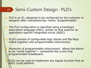
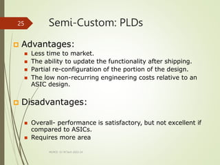
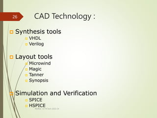
Introducton to CMOS VLSI
MLMCE -S1 M.Tech 2022-24
1
Logical Complexity in ICs
VLSI Design Flow
Design Hieracrchy
Abstraction Level
Regularity, modularity and locality
Semi custom and full custom devices
Reference Text. CMOS VLSI Design , Weste & Harris , Chapter 1, page 31 , chapter
14.2 ,page 620
Growth of Level of Integration
MLMCE -S1 M.Tech 2022-24
2
IC No. of Active
Devices/Transistor/
FET/BJT
Functions Year
SSI 1-100 Gates, OP-Amp, linear App. 1960
MSI 100-1,000 Registers, Filters 1965
LSI 1,000-10,000 Microprocessor, ADC 1970
VLSI 10,000-100,000 Memory, Computers, Signal
Processors
1975
ULSI
GSI
100,000- 40,000,000
40,000,000-50,000,000
Pentium IV.
Dual Core and Quad Core
processors
2001
2011
IC Era (from SSI to VLSI) :
MLMCE -S1 M.Tech 2022-24
3
 IC in 1960s:
 Only 2 transistors and
one resistor.
 Size of chip was more
than required.
 Unable to deal with
complex functionalities.
 Excess power
dissipation.
 Speed/Clock was in
kHz.
 IC in 2014:
 Billions of transistors and
other components.
 Every part of chip is
utilized.
 Efficient in dealing with
complex functionalities.
 Power dissipation brought
in control.
 Million of operations can
be done in just one
second.
Moore's law :
MLMCE -S1 M.Tech 2022-24
4
 Gordon Moore, co-founder of Intel, predicted
about the growth rate of chip complexity in 1960.
 The Law states: The number of transistors that
can be implemented per chip, will doubles after
every 18 months.
 The trend has continued for more than half a
century and is not expected to stop until 2015 or
later.
Logical Complexity in IC :
MLMCE -S1 M.Tech 2022-24
5
 In 1980, at the beginning of VLSI era, the typical
minimum feature size was 2μm.
 A minimum feature size of 0.25 μm was achieved
by 1995.
 Devices with a feature size of 0.18 μm were a
norm in 2001.
 In 2011 feature size was 45nm.
Evolution of Feature Size in IC
over Time
MLMCE -S1 M.Tech 2022-24
6
VLSI Design Flow :
MLMCE -S1 M.Tech 2022-24
7
 Specifications comes first, they
describe abstractly the functionality,
interface, and the architecture of the
digital IC circuit to be designed.
 Behavioral description is then
created to analyze the design in
terms of functionality, performance,
compliance to given standards,
and other specifications.
 RTL description is done using HDLs.
 This RTL description is simulated to
test functionality.
VLSI Design Flow
MLMCE -S1 M.Tech 2022-24
8
 From here onwards we need the
help of EDA tools, synthesis tools.
 RTL description is then converted
to a gate-level netlist using logic
of the circuit in terms of gates
and connections between them,
which are made in such a way
that they meet the timing, power
and area specifications.
 Finally a physical layout is made,
which will be verified and then
sent for fabrication.
VLSI Design Flow:
MLMCE -S1 M.Tech 2022-24
9
Y Chart :
MLMCE -S1 M.Tech 2022-24
10
 The Y-chart consists
of three major
domains, namely:
1. Behavioral domain
2. Structural domain
3. Geometrical layout
domain
Y Chart
MLMCE -S1 M.Tech 2022-24
11
 The design flow starts from the
algorithm that describes the
behavior of the target chip.
 The corresponding architecture
of the processor is first defined.
 It is mapped onto the chip
surface by floorplanning.
 The next design evolution in the
behavioral domain defines finite
state machines (FSMs) which
are structurally implemented
with functional modules such as
registers and arithmetic logic
units (ALUs).
 These modules are then
geometrically placed onto the
chip surface using CAD tools for
automatic module placement
followed by routing, with a goal
of minimizing the interconnects
area and signal delays.
Y Chart
MLMCE -S1 M.Tech 2022-24
12
 The third evolution starts with a
behavioral module description.
Individual modules are then
implemented with leaf cells.
 At this stage the chip is
described in terms of logic gates
(leaf cells), which can be placed
and interconnected by using a
cell placement & routing
program.
 The last evolution involves a
detailed Boolean description of
leaf cells followed by a
transistor level implementation
of leaf cells and mask
generation.
 In standard-cell based design,
leaf cells are already pre-
designed and stored in a library
for logic design use.
Design Hierarchy
MLMCE -S1 M.Tech 2022-24
13
 The use of hierarchy, or ―divide and conquer‖ technique
involves dividing a module into sub- modules and then
repeating this operation on the sub-modules until the
complexity of the smaller parts becomes manageable.
 This approach is very similar to the software case where
large programs are split into smaller and smaller sections
until simple subroutines, with well-defined functions and
interfaces, can be written.
 We know that the design of a VLSI chip can be represented
in three domains.
 Correspondingly, a hierarchy structure can be described in
each domain separately.
Design Hierarchy
MLMCE -S1 M.Tech 2022-24
14
 Example: A CMOS four-bit adder
 The adder can be decomposed progressively into one- bit adders, separate
carry and sum circuits, and finally, into individual logic gates.
 At this lower level of the hierarchy, the design of a simple circuit realizing a
well-defined Boolean function is much more easier to handle than at the
higher levels of the hierarchy.
Design Hierarchy
MLMCE -S1 M.Tech 2022-24
15
 In the physical domain, partitioning a complex
system into its various functional blocks will
provide a valuable guidance for the actual
realization of these blocks on chip.
 Obviously, the approximate shape and size
(area) of each sub-module should be estimated
in order to provide a useful floorplan.
Concepts of Regularity
MLMCE -S1 M.Tech 2022-24
16
 The hierarchical design approach reduces the design complexity by dividing the
large system into several sub-modules.
 Usually, other design concepts and design approaches are also needed to
simplify the process.
 Regularity means that the hierarchical decomposition of a large system should
result in not only simple, but also similar blocks, as much as possible.
 A good example of regularity is the design of array structures consisting of
identical cells - such as a parallel multiplication array, PAL, PLA, PROM.
 Regularity can exist at all levels of abstraction:
 At the transistor level, uniformly sized transistors simplify the design.
 At the logic level, identical gate structures can be used, etc.
 If the designer has a small library of well-defined and well-characterized basic
building blocks, a number of different functions can be constructed by using
this principle.
 Regularity usually reduces the number of different modules that need to be
designed and verified, at all levels of abstraction.
Concepts of Modularity
MLMCE -S1 M.Tech 2022-24
17
 Modularity in design means that the various functional blocks
which make up the larger system must have well-defined
functions and interfaces.
 Modularity allows that each block or module can be designed
relatively independently from each other, since there is no
ambiguity about the function and the signal interface of these
blocks.
 All of the blocks can be combined with ease at the end of the
design process, to form the large system.
 The concept of modularity enables the parallelization of the
design process, reduces development time.
 It also allows the use of generic modules in various designs -
the well-defined functionality and signal interface allow
plug-and-play design.
Concepts of Locality
MLMCE -S1 M.Tech 2022-24
18
 By defining well-characterized interfaces for each module
in the system, we effectively ensure that the internals of
each module become unimportant to the exterior modules.
 Internal details remain at the local level.
 The concept of locality also ensures that connections are
mostly between neighboring modules, avoiding long-
distance connections as much as possible.
 This last point is extremely important for avoiding
excessive interconnect delays.
 Time-critical operations should be performed locally,
without
the need to access distant modules or signals.
 If necessary, the replication of some logic may
solve this problem in large system.
Design Methodology :
MLMCE -S1 M.Tech 2022-24
19
 Full Custom Design
 Semi Custom Design
 Standard Cell
 Gate Array
 PLD’s
 SPLD
 CPLD
 FPGA
Full Custom Design :
MLMCE -S1 M.Tech 2022-24
20
 Full-custom design is a methodology for designing IC’s wherein the
layout, geometry, orientation and placement of every transistor is
done individually by the designer.
 Design productivity is very low – typically few tens of transistors
per day per design.
 Full-custom design potentially maximizes the performance of the
chip, and minimizes its area, but is extremely labor-intensive to
implement.
 Full-custom design is limited to ICs that are to be fabricated in
extremely high volumes, notably certain microprocessors (Intel
Pentium µp chip) and a small number of ASICs.
 The main factor affecting the design and production of ASICs is the
high cost of mask sets and the requisite EDA design tools.
 The mask sets are required in order to transfer the ASIC designs
onto the wafer.
Semi-Custom Design : Standard Cell
MLMCE -S1 M.Tech 2022-24
21
 All commonly used logic cells are developed, characterized and
stored in the standard cell library.
 Library may contain few hundred cells like inverters, NAND, NOR
gates, complex AOI gates, DFF, counters…..
 Each gate type can be implemented in several versions to provide
adequate driving capability(fan-out) – inverter gate can have
standard size, double size and quadruple size. Chip designer can
choose one of it, to meet high current, speed and layout density
requirements.
 Designer sends schematic to the fabricator who prepares mask, if
the cells are from his library.
 Hence it is captivated by the company. Larger the library, larger will
be the cost.
 Standard cell guarantees that design will work.
Semi-Custom Design : Gate array
MLMCE -S1 M.Tech 2022-24
22
 A gate array circuit is a prefabricated chip/circuit with no
particular function, in which transistors and other active
devices are placed (unconnected) at regular predefined
positions and manufactured on a wafer, usually called as
master slice.
 Only masks for metallization needs to be created.
 Interconnection pattern for basic logic gates can be stored
in a library for further chip customization.
 This layer is analogous to the copper layer of a printed
circuit board (PCB).
 Gate array master slices are usually prefabricated and
stockpiled in large quantities regardless of customer
orders.
Semi-Custom: Gate array
 Advantages:
 Less time to market. The design and
fabrication according to the individual
customer specifications may be finished in a
shorter time compared with standard cell or
full custom design.
 This approach reduces the mask cost since
fewer custom masks need to be produced.
 Disadvantage:
 Chip size is fixed.
 Lower efficiency as most of the transistors may
not be in use.
MLMCE -S1 M.Tech 2022-24
23
 However this style is suitable for low production volumes.
Semi-Custom Design : PLD’s
MLMCE -S1 M.Tech 2022-24
24
 PLD is an IC, designed to be configured by the customer or
designer after manufacturing—hence "programmable".
 The PLD configuration is specified using a hardware
description language (HDL), similar to that used for an
application-specific integrated circuit (ASIC).
 PLD’s consists of configurable logic blocks and flip-flops
linked together with programmable interconnect.
 Hierarchy of programmable interconnect allows the blocks
to be "wired together"— somewhat like a one-chip
programmable breadboard.
 PLDs can be used to implement any logical function that an
ASIC could perform.
Semi-Custom: PLDs
MLMCE -S1 M.Tech 2022-24
25
 Advantages:
 Less time to market.
 The ability to update the functionality after shipping.
 Partial re-configuration of the portion of the design.
 The low non-recurring engineering costs relative to an
ASIC design.
 Disadvantages:
 Overall- performance is satisfactory, but not excellent if
compared to ASICs.
 Requires more area
CAD Technology :
MLMCE -S1 M.Tech 2022-24
26
 Synthesis tools
 VHDL
 Verilog
 Layout tools
 Microwind
 Magic
 Tanner
 Synopsis
 Simulation and Verification
 SPICE
 HSPICE
Thank You
MLMCE -S1 M.Tech 2022-24
27

introduction to cmos vlsi

  • 1.
    Introducton to CMOSVLSI MLMCE -S1 M.Tech 2022-24 1 Logical Complexity in ICs VLSI Design Flow Design Hieracrchy Abstraction Level Regularity, modularity and locality Semi custom and full custom devices Reference Text. CMOS VLSI Design , Weste & Harris , Chapter 1, page 31 , chapter 14.2 ,page 620
  • 2.
    Growth of Levelof Integration MLMCE -S1 M.Tech 2022-24 2 IC No. of Active Devices/Transistor/ FET/BJT Functions Year SSI 1-100 Gates, OP-Amp, linear App. 1960 MSI 100-1,000 Registers, Filters 1965 LSI 1,000-10,000 Microprocessor, ADC 1970 VLSI 10,000-100,000 Memory, Computers, Signal Processors 1975 ULSI GSI 100,000- 40,000,000 40,000,000-50,000,000 Pentium IV. Dual Core and Quad Core processors 2001 2011
  • 3.
    IC Era (fromSSI to VLSI) : MLMCE -S1 M.Tech 2022-24 3  IC in 1960s:  Only 2 transistors and one resistor.  Size of chip was more than required.  Unable to deal with complex functionalities.  Excess power dissipation.  Speed/Clock was in kHz.  IC in 2014:  Billions of transistors and other components.  Every part of chip is utilized.  Efficient in dealing with complex functionalities.  Power dissipation brought in control.  Million of operations can be done in just one second.
  • 4.
    Moore's law : MLMCE-S1 M.Tech 2022-24 4  Gordon Moore, co-founder of Intel, predicted about the growth rate of chip complexity in 1960.  The Law states: The number of transistors that can be implemented per chip, will doubles after every 18 months.  The trend has continued for more than half a century and is not expected to stop until 2015 or later.
  • 5.
    Logical Complexity inIC : MLMCE -S1 M.Tech 2022-24 5  In 1980, at the beginning of VLSI era, the typical minimum feature size was 2μm.  A minimum feature size of 0.25 μm was achieved by 1995.  Devices with a feature size of 0.18 μm were a norm in 2001.  In 2011 feature size was 45nm.
  • 6.
    Evolution of FeatureSize in IC over Time MLMCE -S1 M.Tech 2022-24 6
  • 7.
    VLSI Design Flow: MLMCE -S1 M.Tech 2022-24 7  Specifications comes first, they describe abstractly the functionality, interface, and the architecture of the digital IC circuit to be designed.  Behavioral description is then created to analyze the design in terms of functionality, performance, compliance to given standards, and other specifications.  RTL description is done using HDLs.  This RTL description is simulated to test functionality.
  • 8.
    VLSI Design Flow MLMCE-S1 M.Tech 2022-24 8  From here onwards we need the help of EDA tools, synthesis tools.  RTL description is then converted to a gate-level netlist using logic of the circuit in terms of gates and connections between them, which are made in such a way that they meet the timing, power and area specifications.  Finally a physical layout is made, which will be verified and then sent for fabrication.
  • 9.
    VLSI Design Flow: MLMCE-S1 M.Tech 2022-24 9
  • 10.
    Y Chart : MLMCE-S1 M.Tech 2022-24 10  The Y-chart consists of three major domains, namely: 1. Behavioral domain 2. Structural domain 3. Geometrical layout domain
  • 11.
    Y Chart MLMCE -S1M.Tech 2022-24 11  The design flow starts from the algorithm that describes the behavior of the target chip.  The corresponding architecture of the processor is first defined.  It is mapped onto the chip surface by floorplanning.  The next design evolution in the behavioral domain defines finite state machines (FSMs) which are structurally implemented with functional modules such as registers and arithmetic logic units (ALUs).  These modules are then geometrically placed onto the chip surface using CAD tools for automatic module placement followed by routing, with a goal of minimizing the interconnects area and signal delays.
  • 12.
    Y Chart MLMCE -S1M.Tech 2022-24 12  The third evolution starts with a behavioral module description. Individual modules are then implemented with leaf cells.  At this stage the chip is described in terms of logic gates (leaf cells), which can be placed and interconnected by using a cell placement & routing program.  The last evolution involves a detailed Boolean description of leaf cells followed by a transistor level implementation of leaf cells and mask generation.  In standard-cell based design, leaf cells are already pre- designed and stored in a library for logic design use.
  • 13.
    Design Hierarchy MLMCE -S1M.Tech 2022-24 13  The use of hierarchy, or ―divide and conquer‖ technique involves dividing a module into sub- modules and then repeating this operation on the sub-modules until the complexity of the smaller parts becomes manageable.  This approach is very similar to the software case where large programs are split into smaller and smaller sections until simple subroutines, with well-defined functions and interfaces, can be written.  We know that the design of a VLSI chip can be represented in three domains.  Correspondingly, a hierarchy structure can be described in each domain separately.
  • 14.
    Design Hierarchy MLMCE -S1M.Tech 2022-24 14  Example: A CMOS four-bit adder  The adder can be decomposed progressively into one- bit adders, separate carry and sum circuits, and finally, into individual logic gates.  At this lower level of the hierarchy, the design of a simple circuit realizing a well-defined Boolean function is much more easier to handle than at the higher levels of the hierarchy.
  • 15.
    Design Hierarchy MLMCE -S1M.Tech 2022-24 15  In the physical domain, partitioning a complex system into its various functional blocks will provide a valuable guidance for the actual realization of these blocks on chip.  Obviously, the approximate shape and size (area) of each sub-module should be estimated in order to provide a useful floorplan.
  • 16.
    Concepts of Regularity MLMCE-S1 M.Tech 2022-24 16  The hierarchical design approach reduces the design complexity by dividing the large system into several sub-modules.  Usually, other design concepts and design approaches are also needed to simplify the process.  Regularity means that the hierarchical decomposition of a large system should result in not only simple, but also similar blocks, as much as possible.  A good example of regularity is the design of array structures consisting of identical cells - such as a parallel multiplication array, PAL, PLA, PROM.  Regularity can exist at all levels of abstraction:  At the transistor level, uniformly sized transistors simplify the design.  At the logic level, identical gate structures can be used, etc.  If the designer has a small library of well-defined and well-characterized basic building blocks, a number of different functions can be constructed by using this principle.  Regularity usually reduces the number of different modules that need to be designed and verified, at all levels of abstraction.
  • 17.
    Concepts of Modularity MLMCE-S1 M.Tech 2022-24 17  Modularity in design means that the various functional blocks which make up the larger system must have well-defined functions and interfaces.  Modularity allows that each block or module can be designed relatively independently from each other, since there is no ambiguity about the function and the signal interface of these blocks.  All of the blocks can be combined with ease at the end of the design process, to form the large system.  The concept of modularity enables the parallelization of the design process, reduces development time.  It also allows the use of generic modules in various designs - the well-defined functionality and signal interface allow plug-and-play design.
  • 18.
    Concepts of Locality MLMCE-S1 M.Tech 2022-24 18  By defining well-characterized interfaces for each module in the system, we effectively ensure that the internals of each module become unimportant to the exterior modules.  Internal details remain at the local level.  The concept of locality also ensures that connections are mostly between neighboring modules, avoiding long- distance connections as much as possible.  This last point is extremely important for avoiding excessive interconnect delays.  Time-critical operations should be performed locally, without the need to access distant modules or signals.  If necessary, the replication of some logic may solve this problem in large system.
  • 19.
    Design Methodology : MLMCE-S1 M.Tech 2022-24 19  Full Custom Design  Semi Custom Design  Standard Cell  Gate Array  PLD’s  SPLD  CPLD  FPGA
  • 20.
    Full Custom Design: MLMCE -S1 M.Tech 2022-24 20  Full-custom design is a methodology for designing IC’s wherein the layout, geometry, orientation and placement of every transistor is done individually by the designer.  Design productivity is very low – typically few tens of transistors per day per design.  Full-custom design potentially maximizes the performance of the chip, and minimizes its area, but is extremely labor-intensive to implement.  Full-custom design is limited to ICs that are to be fabricated in extremely high volumes, notably certain microprocessors (Intel Pentium µp chip) and a small number of ASICs.  The main factor affecting the design and production of ASICs is the high cost of mask sets and the requisite EDA design tools.  The mask sets are required in order to transfer the ASIC designs onto the wafer.
  • 21.
    Semi-Custom Design :Standard Cell MLMCE -S1 M.Tech 2022-24 21  All commonly used logic cells are developed, characterized and stored in the standard cell library.  Library may contain few hundred cells like inverters, NAND, NOR gates, complex AOI gates, DFF, counters…..  Each gate type can be implemented in several versions to provide adequate driving capability(fan-out) – inverter gate can have standard size, double size and quadruple size. Chip designer can choose one of it, to meet high current, speed and layout density requirements.  Designer sends schematic to the fabricator who prepares mask, if the cells are from his library.  Hence it is captivated by the company. Larger the library, larger will be the cost.  Standard cell guarantees that design will work.
  • 22.
    Semi-Custom Design :Gate array MLMCE -S1 M.Tech 2022-24 22  A gate array circuit is a prefabricated chip/circuit with no particular function, in which transistors and other active devices are placed (unconnected) at regular predefined positions and manufactured on a wafer, usually called as master slice.  Only masks for metallization needs to be created.  Interconnection pattern for basic logic gates can be stored in a library for further chip customization.  This layer is analogous to the copper layer of a printed circuit board (PCB).  Gate array master slices are usually prefabricated and stockpiled in large quantities regardless of customer orders.
  • 23.
    Semi-Custom: Gate array Advantages:  Less time to market. The design and fabrication according to the individual customer specifications may be finished in a shorter time compared with standard cell or full custom design.  This approach reduces the mask cost since fewer custom masks need to be produced.  Disadvantage:  Chip size is fixed.  Lower efficiency as most of the transistors may not be in use. MLMCE -S1 M.Tech 2022-24 23  However this style is suitable for low production volumes.
  • 24.
    Semi-Custom Design :PLD’s MLMCE -S1 M.Tech 2022-24 24  PLD is an IC, designed to be configured by the customer or designer after manufacturing—hence "programmable".  The PLD configuration is specified using a hardware description language (HDL), similar to that used for an application-specific integrated circuit (ASIC).  PLD’s consists of configurable logic blocks and flip-flops linked together with programmable interconnect.  Hierarchy of programmable interconnect allows the blocks to be "wired together"— somewhat like a one-chip programmable breadboard.  PLDs can be used to implement any logical function that an ASIC could perform.
  • 25.
    Semi-Custom: PLDs MLMCE -S1M.Tech 2022-24 25  Advantages:  Less time to market.  The ability to update the functionality after shipping.  Partial re-configuration of the portion of the design.  The low non-recurring engineering costs relative to an ASIC design.  Disadvantages:  Overall- performance is satisfactory, but not excellent if compared to ASICs.  Requires more area
  • 26.
    CAD Technology : MLMCE-S1 M.Tech 2022-24 26  Synthesis tools  VHDL  Verilog  Layout tools  Microwind  Magic  Tanner  Synopsis  Simulation and Verification  SPICE  HSPICE
  • 27.
    Thank You MLMCE -S1M.Tech 2022-24 27