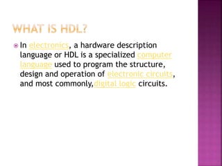
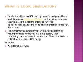
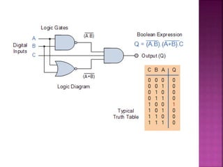
This document discusses hardware description languages used in electronics design. It describes how HDLs like VHDL and Verilog are used to program digital and mixed-signal circuits. Simulation allows validation of the design against specifications. The document also discusses formal verification using property specification languages and different modeling styles for Verilog like gate-level, dataflow, and behavioral modeling.
FPGA are a special form of Programmable logic devices(PLDs) with higher densities as compared to custom ICs and capable of implementing functionality in a short period of time using computer aided design (CAD) software....by mathewsubin3388@gmail.com
Complex Programmable Logic Device (CPLD) Architecture and Its Applicationselprocus
A CPLD (complex programmable logic device) chip includes several circuit blocks on a single chip with inside wiring resources to attach the circuit blocks. Each circuit block is comparable to a PLA or a PAL.
Those slides describe digital design using Verilog HDL,
starting with Design methodologies for any digital circuit then difference between s/w (C/C++) and H/w (Verilog) and the most important constructs that let us start hardware design using Verilog HDL.
Field-programmable gate array\
only for these students that are intrested in Field-programmable gate array
field-programmable gate array (FPGA) is an integrated circuit designed to be configured by a customer or a designer after manufacturing – hence "field-programmable". The FPGA configuration is generally specified using a hardware description language (HDL), similar to that used for an application-specific integrated circuit (ASIC). (Circuit diagrams were previously used to specify the configuration, as they were for ASICs
The FPGA industry sprouted from programmable read-only memory (PROM) and programmable logic devices (PLDs). PROMs and PLDs both had the option of being programmed in batches in a factory or in the field (field-programmable). However, programmable logic was hard-wired between logic gates.[6]
In the late 1980s, the Naval Surface Warfare Center funded an experiment proposed by Steve Casselman to develop a computer that would implement 600,000 reprogrammable gates. Casselman was successful and a patent related to the system was issued in 1992.[6]
Some of the industry's foundational concepts and technologies for programmable logic arrays, gates, and logic blocks are founded in patents awarded to David W. Page and LuVerne R. Peterson in 1985.
I made this presentation for you , I hope its useful for you all, and I hate Plagiarism please, I also used some slides here but I mentioned all in the last slide :)
Hope you can get benefits from it
This presentation gives an overview of FPGA devices. An FPGA is a device that contains a matrix of re-configurable gate array logic circuitry. When a FPGA is configured, the internal circuitry is connected in a way that creates a hardware implementation of the software application.
FPGA devices can deliver the performance and reliability of dedicated hardware circuitry.
1) What are the digital design entry methods Form your opinion, whi.pdffasttrackscardecors
1) What are the digital design entry methods? Form your opinion, which one is the most
efficient? Why?
2) What is the difference between a functional simulation and a timing simulation? Is a
functional simulation sufficient enough to ensure the correctness of the design?
Solution
There are following data entry methods:
1 Schematic capture
2 Hardware Description Language (HDL) capture (VHDL, Verilog)
Schematic capture :
Schematic capture is a step in the designing of electronic design automation (EDA) at which the
electronic diagram of the electronic circuit is created by a designer. This is done with the help of
a schematic capture tool also known as schematic editor.
The circuit design is the very first step of actual design of an electronic circuit. It involves
drawing sketches on paper, and then entered into a computer using a schematic editor.
Hardware Description Language (HDL) capture (VHDL, Verilog) :
a. Hardware description language (HDL) is a specialized computer language used to describe the
structure and behavior of electronic circuits.
b. It enables a precise, formal description of an electronic circuit that allows for the automated
analysis and simulation of an electronic circuit.
c. There are currently two main Hardware Descriptive Languages, VHDL and Verilog.
d. Verilog syntax is not as complicated as VHDL and is less verbose. It lacks features and
capabilities that VHDL can provide.
e. Verilog is easier to grasp and understand and its constructs are based on 50% C programming
and 50% ADA.
Which approach should be used :
a. The hardware description language (HDL) is used at the industry level.
b. HDL allows the designer to organize and integrate complex functions and verify the
individual blocks and eventually the entire design with tools like HDL simulators.
c. Schematic capture was a typical design approach was used before but when the average gate
count passed the 10,000 gate threshold, they started to break down.
Functional simulators and Timing simulators :
a. Functional simulators verify the logical behavior of a design based on design entry.
b. Timing simulators perform timing verifications at multiple stages of the design. In this
simulation the real behavior of the system is verified when encountering the circuit delays and
circuit elements in actual device.
As Functional Simulation simply tests the logic \"functional\" operation of the circuit. There is
no consideration for delay through the internal logic, We should also use Timing simulation to
ensure the correctness of the design.
With Timing Simulation, the delay asociated with the logic elements and the interconnect
routing are taken into consideration..
FPGA, VLSI design flow using HDL, introduction to behavior, logic and physica...Rup Chowdhury
Field-Programmable Gate Arrays (FPGAs) and Very Large Scale Integration (VLSI) design play pivotal roles in the development of modern electronic systems, offering a flexible and efficient platform for implementing complex digital circuits. This description delves into the world of FPGA and VLSI design flow using Hardware Description Languages (HDL) and introduces the crucial concepts of behavior, logic, and physical synthesis.
FPGA Overview:
FPGAs are reconfigurable semiconductor devices that allow designers to implement custom digital circuits, making them ideal for prototyping, rapid development, and applications requiring flexibility. They consist of an array of programmable logic blocks, configurable interconnects, and memory elements, providing a versatile hardware platform.
VLSI Design Flow using HDL:
The VLSI design flow is a systematic process employed by engineers to design, implement, and verify integrated circuits. Hardware description languages, such as Verilog and VHDL, are essential components of this flow. These languages enable designers to express the functionality and structure of digital circuits in a human-readable and simulation-friendly manner.
VHDL stands for very high speed integrated circuit hardware description language and used to design and simulate basic as well as complex digital circuits.
CETPA INFOTECH PVT LTD is one of the IT education and training service provider brands of India that is preferably working in 3 most important domains. It includes IT Training services, software and embedded product development and consulting services.
http://www.cetpainfotech.com
VHDL is defined by IEEE. This standard is known by all the VHDL tool developers. So
there is only one language to learn. This language is used by all the circuit designers around the world. The life time for this language is assured, since it is an IEEE standards. Any investment or learning is assured for lifetime. Abundance of models available from different sources can be used with ease. Some tools might support Foreign Language Interface, by which you can add your model in C language to the VHDL code. It is a modern language, powerful and general. Other advantages include readability of the code and portability. The code developed is portable to any technology at any time. Time to market is short (leads to leadership in the market). Any error found during the simulation phase is less expensive than by discovering the errors after making the circuit board (Investment is saved). The great advantage is that the Project Managers can modify the specification without leading to disaster (only the necessary portion of the code need to be changed). It can deliver designs 100% error free at short duration. New Concepts in
hardware design (for example, in image processing, DSP, etc.,) can be modeled in VHDL and its efficiency or viability can be proven without doing the hardware. A large number of ASICs fail to work when plugged into a system even if they meet their specifications first time. VHDL addresses this issue in two ways: A VHDL specification can be executed in order to achieve a high level of confidence in its correctness before commencing design, and may simulate one to two orders of magnitude faster than a gate level description. A VHDL specification for a part can form the basis for a simulation model to verify the operation of the part in the wider system context (e.g. printed circuit board simulation). This depends on how accurately the specification handles aspects such as timing and initialization.
Similar to HDL (hardware description language) presentation (20)
NO1 Uk Amil Baba In Lahore Kala Jadu In Lahore Best Amil In Lahore Amil In La...Amil baba
Contact with Dawood Bhai Just call on +92322-6382012 and we'll help you. We'll solve all your problems within 12 to 24 hours and with 101% guarantee and with astrology systematic. If you want to take any personal or professional advice then also you can call us on +92322-6382012 , ONLINE LOVE PROBLEM & Other all types of Daily Life Problem's.Then CALL or WHATSAPP us on +92322-6382012 and Get all these problems solutions here by Amil Baba DAWOOD BANGALI
#vashikaranspecialist #astrologer #palmistry #amliyaat #taweez #manpasandshadi #horoscope #spiritual #lovelife #lovespell #marriagespell#aamilbabainpakistan #amilbabainkarachi #powerfullblackmagicspell #kalajadumantarspecialist #realamilbaba #AmilbabainPakistan #astrologerincanada #astrologerindubai #lovespellsmaster #kalajaduspecialist #lovespellsthatwork #aamilbabainlahore#blackmagicformarriage #aamilbaba #kalajadu #kalailam #taweez #wazifaexpert #jadumantar #vashikaranspecialist #astrologer #palmistry #amliyaat #taweez #manpasandshadi #horoscope #spiritual #lovelife #lovespell #marriagespell#aamilbabainpakistan #amilbabainkarachi #powerfullblackmagicspell #kalajadumantarspecialist #realamilbaba #AmilbabainPakistan #astrologerincanada #astrologerindubai #lovespellsmaster #kalajaduspecialist #lovespellsthatwork #aamilbabainlahore #blackmagicforlove #blackmagicformarriage #aamilbaba #kalajadu #kalailam #taweez #wazifaexpert #jadumantar #vashikaranspecialist #astrologer #palmistry #amliyaat #taweez #manpasandshadi #horoscope #spiritual #lovelife #lovespell #marriagespell#aamilbabainpakistan #amilbabainkarachi #powerfullblackmagicspell #kalajadumantarspecialist #realamilbaba #AmilbabainPakistan #astrologerincanada #astrologerindubai #lovespellsmaster #kalajaduspecialist #lovespellsthatwork #aamilbabainlahore #Amilbabainuk #amilbabainspain #amilbabaindubai #Amilbabainnorway #amilbabainkrachi #amilbabainlahore #amilbabaingujranwalan #amilbabainislamabad
MATHEMATICS BRIDGE COURSE (TEN DAYS PLANNER) (FOR CLASS XI STUDENTS GOING TO ...PinkySharma900491
Class khatm kaam kaam karne kk kabhi uske kk innings evening karni nnod ennu Tak add djdhejs a Nissan s isme sniff kaam GCC bagg GB g ghan HD smart karmathtaa Niven ken many bhej kaam karne Nissan kaam kaam Karo kaam lal mam cell pal xoxo
2. In electronics, a hardware description
language or HDL is a specialized computer
language used to program the structure,
design and operation of electronic circuits,
and most commonly,digital logic circuits.
3. Simulation allows an HDL description of a design (called a
model) to pass design verification, an important milestone
that validates the design's intended function
(specification) against the code implementation in the HDL
description
. The engineer can experiment with design choices by
writing multiple variations of a base design, then
comparing their behavior in simulation. Thus, simulation is
critical for successful HDL design
Example:
Work Bench Software
4. Histrocially,design verification was a laborious,
repetitive loop of writing and running
simulation test cases against the design under
test which takes much time to verify.
The EDA industry developed the Property
Specification Language. A property or properties
can be proven true or false using formal
mathematical methods.
6. VHDL (V Hardware Description Language) is a
hardware description language used in electronic
design automation to describe digital and mixed-
signal systems such as field-programmable gate
arrays and integrated circuits
Advantage:
VHDL is a dataflow language, unlike procedural
computing languages such as BASIC, C, and
assembly code, which all run sequentially, one
instruction at a time.
7. Hardware description languages such as
Verilog differ from software programming
languages because they include ways of
describing the propagation of time and signal
dependencies (sensitivity).
Now a day there is no use of verilog HDL.
8. The module is the basic building bloak f0r
modeling hardware with the VerilogHDL. The
logic of a module can be described in any
one (or a combination) of the following
modeling styles
Gate-level modeling
Dataflow modeling
Behavioral modelings
9. A logic network can be modeled using
continuous assignments or switches and logic
gates. Gates and continuous assignments
serve different modeling purposes and it is
important to appreciate the differences
between them in order to achieve the right
balance between accuracy and efficiency in
Verilog-XL
10. Dataflow modeling provides a powerful way
to implement a design. Verilog allows a
design processes data rather than
instantiation of individual gates. Dataflow
modeling has become a popular design
approach as logic synthesis tools have
become sophisticated. This approach allows
the designer to concentrate on optimizing
the circuit in terms of data flow.
11. Verilog behavioral models contain procedural
statements that control the simulation and
manipulate variables of the data types
previously described. These statements are
contained within procedures. Each procedure
has an activity flow associated with it.