HAS: HIGH SPEED & POWER EFFICIENT HYBRID ADDER/SUBTRACTOR DESIGN USING REVERSIBLE LOGIC
•
0 likes•2 views

https://www.irjet.net/archives/V9/i1/IRJET-V9I109.pdf

Recommended
Recommended
More Related Content
Similar to HAS: HIGH SPEED & POWER EFFICIENT HYBRID ADDER/SUBTRACTOR DESIGN USING REVERSIBLE LOGIC
Similar to HAS: HIGH SPEED & POWER EFFICIENT HYBRID ADDER/SUBTRACTOR DESIGN USING REVERSIBLE LOGIC (20)
More from IRJET Journal
More from IRJET Journal (20)
Recently uploaded
Recently uploaded (20)
HAS: HIGH SPEED & POWER EFFICIENT HYBRID ADDER/SUBTRACTOR DESIGN USING REVERSIBLE LOGIC
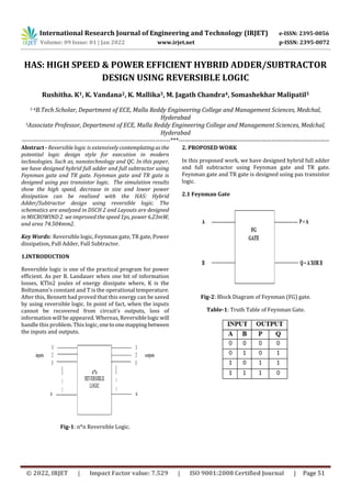
- 1. International Research Journal of Engineering and Technology (IRJET) e-ISSN: 2395-0056 Volume: 09 Issue: 01 | Jan 2022 www.irjet.net p-ISSN: 2395-0072 HAS: HIGH SPEED & POWER EFFICIENT HYBRID ADDER/SUBTRACTOR DESIGN USING REVERSIBLE LOGIC Rushitha. K1, K. Vandana2, K. Mallika3, M. Jagath Chandra4, Somashekhar Malipatil5 1-4B.Tech Scholar, Department of ECE, Malla Reddy Engineering College and Management Sciences, Medchal, Hyderabad 5Associate Professor, Department of ECE, Malla Reddy Engineering College and Management Sciences, Medchal, Hyderabad ---------------------------------------------------------------------***---------------------------------------------------------------------- Abstract - Reversible logic is extensively contemplatingasthe potential logic design style for execution in modern technologies. Such as, nanotechnology and QC. In this paper, we have designed hybrid full adder and full subtractor using Feynman gate and TR gate. Feynman gate and TR gate is designed using pas transistor logic. The simulation results show the high speed, decrease in size and lower power dissipation can be realized with the HAS: Hybrid Adder/Subtractor design using reversible logic. The schematics are analyzed in DSCH 2 and Layouts are designed in MICROWIND 2. we improved the speed 1ps, power 6.23mW, and area 74.504mm2. Key Words: Reversible logic, Feynman gate, TR gate, Power dissipation, Full Adder, Full Subtractor. 1.INTRODUCTION Reversible logic is one of the practical program for power efficient. As per R. Landauer when one bit of information losses, KTln2 joules of energy dissipate where, K is the Boltzmann’s constant and T is the operational temperature. After this, Bennett had proved that this energy can be saved by using reversible logic. In point of fact, when the inputs cannot be recovered from circuit’s outputs, loss of information will be appeared. Whereas, Reversiblelogicwill handle this problem. This logic, onetoonemappingbetween the inputs and outputs. Fig-1: n*n Reversible Logic. 2. PROPOSED WORK In this proposed work, we have designed hybrid full adder and full subtractor using Feynman gate and TR gate. Feynman gate and TR gate is designed using pas transistor logic. 2.1 Feynman Gate Fig-2: Block Diagram of Feynman (FG) gate. Table-1: Truth Table of Feynman Gate. © 2022, IRJET | Impact Factor value: 7.529 | ISO 9001:2008 Certified Journal | Page 51
- 2. International Research Journal of Engineering and Technology (IRJET) e-ISSN: 2395-0056 Volume: 09 Issue: 01 | Jan 2022 www.irjet.net p-ISSN: 2395-0072 Fig-3: Schematic of FG Gate The above figure shows schematic of the Feynman(FG) gate. The Feynman gate is also known as controlled- not gate (CNOT). It has two inputs i.e., A and B and two outputs i.e., P and Q. The outputs are given as P=A, and Q=A XOR B. which realizes XOR gate with a garbage output ‘A’. If B=‘0’ it replicates the input ‘A’ and if B=‘1’, then it transpose the input ‘A’ to the output Q. The pass transistor realization of Feynman gate is shown in figure 2. Consider inputs as a=‘1’ and b=‘1’, then the transistors Q2, Q4 and Q6 are ON and the remaining transistors are OFF. So theVddvalue‘1’isdirectly passed to the output ‘p’ and the ground value ‘0’ is passed to the output q. So, p=‘1’ and q=‘0’ 2.2 TR Gate Fig-4: Block Diagram of TR gate. Table-2: Truth Table of TR Gate Fig-5: Schematic of TR Gate The above Figure represents the schematic ofhybrid TR gate with A, B, C as inputs and P, Q, R as outputs, where P=A, Q=A⊕B and R=AB’⊕C. This gate is proposed by Toffoli and Ranganathan. The figure 12 shows the CMOS realization of TR gate. The pass transistor realization of TR gate is shown in above figure Consider the inputs are a=‘1’, b=‘1’, c=‘0’. Since a=‘1’ the transistor Q1 is OFF and Q2 is ON. So the output p=‘1’. Since a=‘1’ and b=‘1’, Q4, Q8 are ON and Q3, Q7 are OFF. So the ground value ‘0’ is passed through Q4, Q8 then the output q=‘0’. Since a=‘1’, b=‘1’andc=‘0’,thenQ6, Q9, Q12 are ON and Q5, Q10, Q11 are OFF. So the ground value ‘0’ is passed through Q10, Q12 then the output r=‘0’. © 2022, IRJET | Impact Factor value: 7.529 | ISO 9001:2008 Certified Journal | Page 52
- 3. International Research Journal of Engineering and Technology (IRJET) e-ISSN: 2395-0056 Volume: 09 Issue: 01 | Jan 2022 www.irjet.net p-ISSN: 2395-0072 2.3 Hybrid Half Adder/Subtractor Fig-6: Block Diagram of Hybrid Half Adder/Subtractor Table-3: Truth Table of Hybrid Half Adder/Subtractor Fig-7: Schematic of Hybrid Half Subtractor Fig-8: Schematic of Hybrid Half Adder. In the hybrid half Adder/Subtractar we use two different types of Gates: which are namely FEYNMAN Gate and TR Gate. The above schematic shows the combinations of two FG gate’s and with one TR gate. Where one FG gate has two inputs and two outputs, in this FG 1 gateofBinputis connected to FG 2 gate of 1st input as shown inaboveFigure and 2nd input is taken as control gate. This control gate is switches to one and zero based on its input, it acts as half adder/subtractar. The FG 1 gate of Q output is connected with a LED that shows the Sum/Difference andFG1gateofP output is connected to the input of TR gate as shown in above figure. Although, the FG 2 gate of Q output is connected to B input of TR gate and TR gate C input is connected to ground, since output is taken out from R with LED which is Carry/Borrow. When the control (CTRL) is in ON conditionitactsasa half adder i.e., CTRL=1. When we give input as ‘0’ to the both inputs A and B we get ‘0’ as a output in both sum and carry i.e., both LEDs will be in off condition. Similarly, When we give inputs ‘0’ and ‘1’ to the A and B therefore the outputs will be ‘1’in sum and ‘0’ in carry i.e., sum LED will be ON and carry LED will be OFF. When 1 and 0 inputs are given to A & B the sum LEDs will be ON and carry will be OFF. Giving 1 to A and B inputs sum LED will be OFF and carry LED will be ON. When the control (CTRL) is in OFF condition it acts half subtractor i.e., CTRL=0. In this when A & B taken as ‘0’ the difference/Borrow will not be in ON state i.e, LED is in OFF. When A is taken as ‘1’ and B is taken as ‘0’ hence, it's difference LED will be ON and borrow LED will be OFF. When A is taken as ‘0’ and B is taken as ‘1’ the differences LED will be ON and borrow LED will be OFF. WhenAand Bis taken as ‘1’ the difference and borrow LEDs will be OFF. Inputs Adder Outputs (Ctrl=1) Subtractor Outputs (Ctrl=0) A B Sum Carr-Y Diff Borrow 0 0 0 0 0 0 0 1 1 0 1 1 1 0 1 0 1 0 1 1 0 1 0 0 © 2022, IRJET | Impact Factor value: 7.529 | ISO 9001:2008 Certified Journal | Page 53
- 4. International Research Journal of Engineering and Technology (IRJET) e-ISSN: 2395-0056 Volume: 09 Issue: 01 | Jan 2022 www.irjet.net p-ISSN: 2395-0072 2.4 Hybrid Full Adder/Subtractor Fig-9: Block Diagram of Hybrid Full Adder/Subtractor Table-4: Truth Table of Hybrid Full Adder/Subtarctor. Fig-10: Schematic of Hybrid Full Adder. Fig-11: Schematic of Hybrid Full Subtractor. The above figure shows the schematic of the Full Adder/Subtractor. In this operationweusetwoFG gatesand two TR gates with Three inputs that are A,B and Control. When the Control is in ON state it acts as Full adder, A input in FG gate is connected to first input of second FG gate and B input in FG gate is connected to TR first input. C is taken as third input from second TR gate. The outputs of FG gate and TR gate is connected to second TR gate as shown in figure. Sum/Difference is taken out from the second TR gate where is LED is connected and Carry/Borrow is taken out from the second TR gate where another LED is used here to indicate the operations of full adder and full subtractor. When the inputs are given 000 as input the output will be 00 in sum and carry & vice versa.When the inputs are takenas001,010 and 100 the sum will be in ON so that LED will turn ON. When the inputs are taken as 011,101,110 the carry will be in ON. Coming to Full subtractor it is also provide same output if the 3 inputs are same, then the output will be the input as same the inputs. When the inputs are taken as 001,010 the output will be turned on so the LED will beONIf the input is 011 then only borrow output will be turned on and when the input is 100 then difference output will be ON. 3. RESULTS 3.1 Simulations Fig-12: Simulation of FG Gate © 2022, IRJET | Impact Factor value: 7.529 | ISO 9001:2008 Certified Journal | Page 54
- 5. International Research Journal of Engineering and Technology (IRJET) e-ISSN: 2395-0056 Volume: 09 Issue: 01 | Jan 2022 www.irjet.net p-ISSN: 2395-0072 Fig-13: Simulation of TR Gate Fig-14: Analog Simulation of half Adder/ Subtractor Fig-15: Analog Simulation of Hybrid full Adder/Subtractor 3.2 Layouts and 3D views Fig-16: Layout of Hybrid Half Adder/Subtractor Fig-17: 3D view of Hybrid Full Adder/Subtractor Fig-18: Layout of Hybrid Full Adder/Subtractor © 2022, IRJET | Impact Factor value: 7.529 | ISO 9001:2008 Certified Journal | Page 55
- 6. International Research Journal of Engineering and Technology (IRJET) e-ISSN: 2395-0056 Volume: 09 Issue: 01 | Jan 2022 www.irjet.net p-ISSN: 2395-0072 Fig-19: 3D View of Hybrid Full Adder/Subtractor 3.3 Power Analysis Hybrid Half Adder/Subtractor 0.352mwatts. Hybrid Full Adder/Subtractor 6.253mwatts. 3.4 Area Analysis Hybrid Half Adder/Subtractor Area=376um*129um =48.504mm2 Hybrid Full Adder/Subtractor Area=556um*134um =74.504mm2 3.5 Delay Analysis 1pz 4. CONCLUSION In this paper, we have designed hybrid adder/subtractor using reversible logic. we have enhanced the speed 1ps and optimized the power 6.23mW and area 74.504mm2. The total layout is reduced by using less number of transistors and simulated in Microwind 2. REFERENCES [1] R. Landauer., Irreversibility and heat generation in the computing process,IBMJournal ofResearchand Development, vol. 5, no. 3, pp. 183 191, July 1961. [2] C. Bennett, Logical reversibilityofcomputation,IBM Journal of Research and Development, vol. 17,no.6, pp. 525532, Nov 1973. [3] S. K. S. Hari, S. Shroff, S. Mahammad, and V. Kamakoti, Efficient building blocks for reversible sequential circuit design, in Circuits and Systems, 2006. MWSCAS 06. 49th IEEE International Midwest Symposium on, vol. 1, Aug 2006, pp. 437441. [4] J. Bruce, M. Thornton, L. Shivakumaraiah, P. Kokate, and X. Li, Efficient adder circuits based on a conservative reversible logic gate, in VLSI, 2002. Proceedings. IEEE Computer Society Annual Symposium on, 2002, pp. 7479. [5] Somashekhar Malipatil, R. Basavaraju and Praveen Kumar Nartam. "Low Power & High Speed Carry Select Adder Design Using Verilog" IOSR Journal of VLSI and Signal Processing Vol. 6 Iss. 6 (2016) p. 77 - 81 ISSN: 2319 – 4197. [6] Somashekhar Malipatil, Avinash Gour, Vikas Maheshwari, FPGA Implementation of Fault Tolerant & High Speed Reversible Systolic Multiplier Volume 09, Issue 12, Pages: 537-542. DOI: 10.48047/IJIEMR/V09/I12/95. [7] Somashekhar Malipatil, Avinash Gour and Vikas Maheshwari, Design & Implementation of Reconfigurable Adaptive Fault Tolerant SystemFor ALU, International Journal of Electrical Engineering and Technology, 11(9), 2020, pp. 01-07. [8] D. Maslov, G. Dueck, and D. Miller, Synthesis of fredkin-toffoli reversible networks, Very Large- Scale Integration (VLSI)Systems,IEEETransactions on, vol. 13, no. 6, pp. 765769, June 2005. [9] P. Kaur and B. Dhaliwal, Design of fault tolerant full adder/subtractor using reversible gates, in Computer Communication and Informatics (ICCCI), 2012. [10] S. Malipatil, A. Gour and V. Maheshwari, "Fault Tolerant Reversible Full Adder Design Using Gate Diffusion Input," 2020 International Conference on Smart Technologies in Computing, Electrical and Electronics (ICSTCEE), 2020, pp. 120-123, doi: 10.1109/ICSTCEE49637.2020.9276774. [11] S. Malipatil, V. Maheshwari andM.B.Chandra,"Area Optimization Of CMOS Full Adder Design Using 3t Xor," 2020 International Conference On Wireless CommunicationsSignal ProcessingAndNetworking (Wispnet), 2020, Pp. 192-194, Doi: 10.1109/Wispnet48689.2020.9198627. [12] Somashekhar Malipatil, Vikas Maheshwari andR.P. Singh, "FPGA Implementation of Fault Tolerant Adder using Verilog for High Speed VLSI Architectures", International Journal ofEngineering and Advanced Technology (IJEAT), vol. 9, no. 4, April 2020, ISSN 2249–8958. © 2022, IRJET | Impact Factor value: 7.529 | ISO 9001:2008 Certified Journal | Page 56