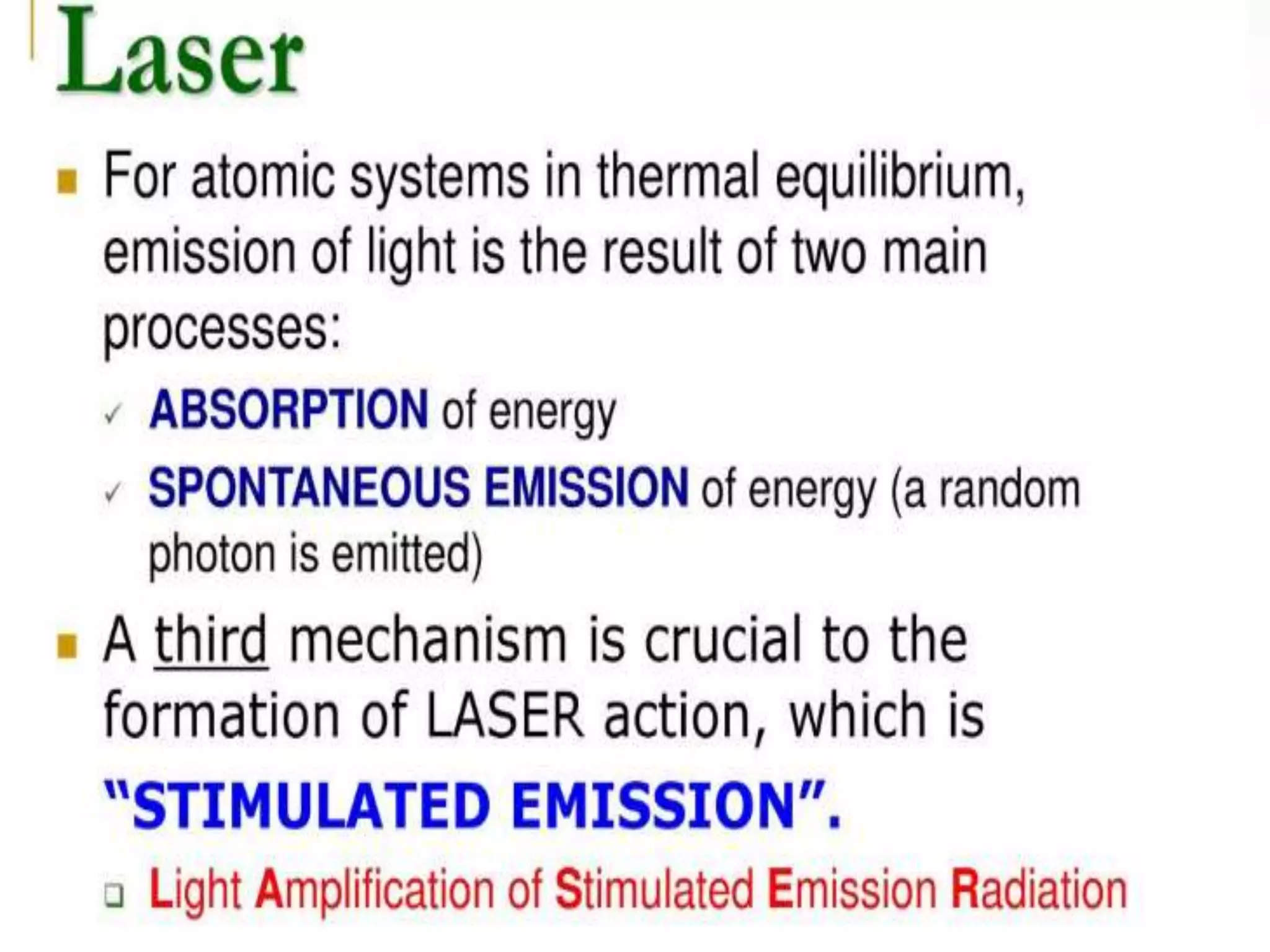
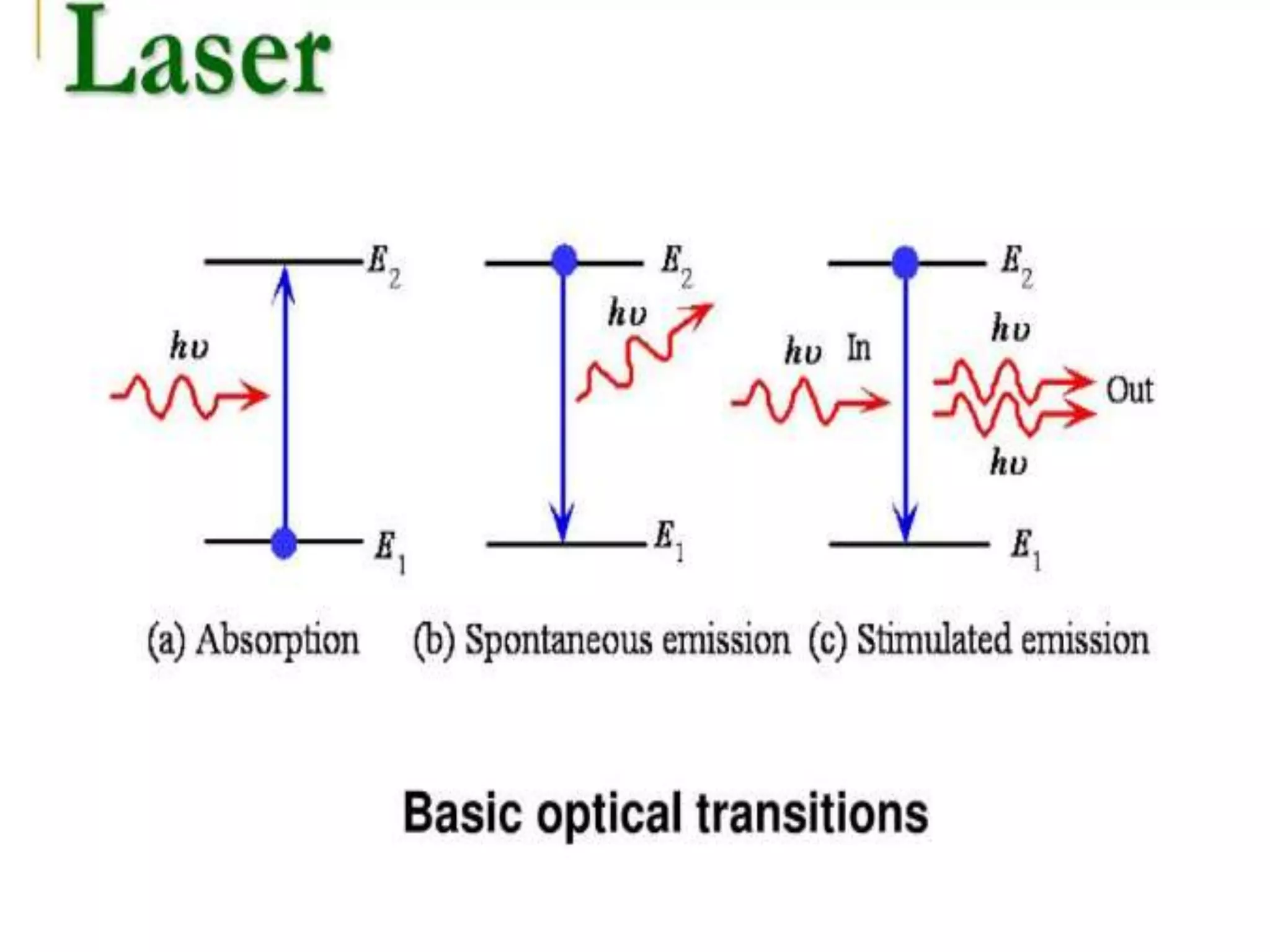
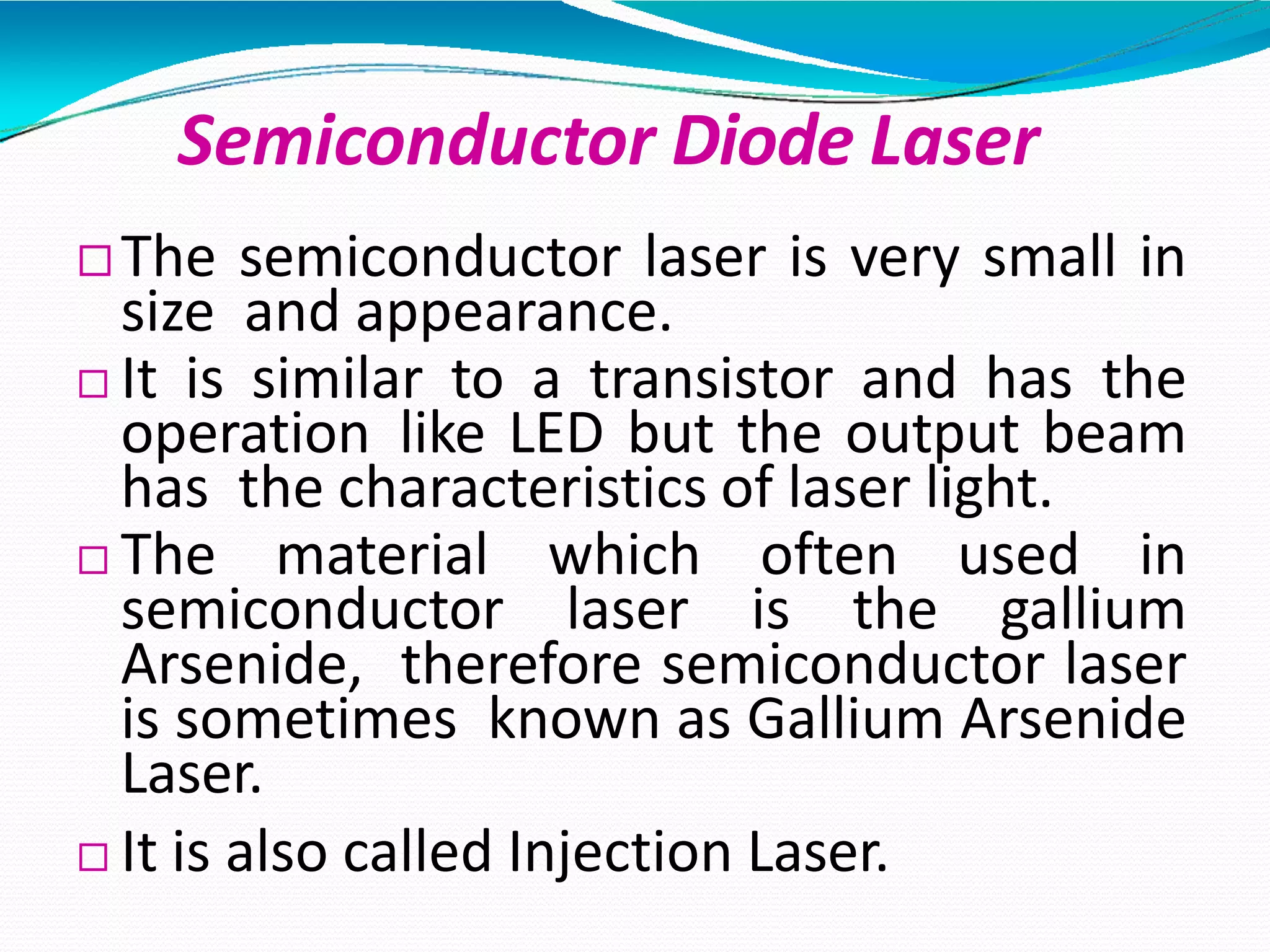
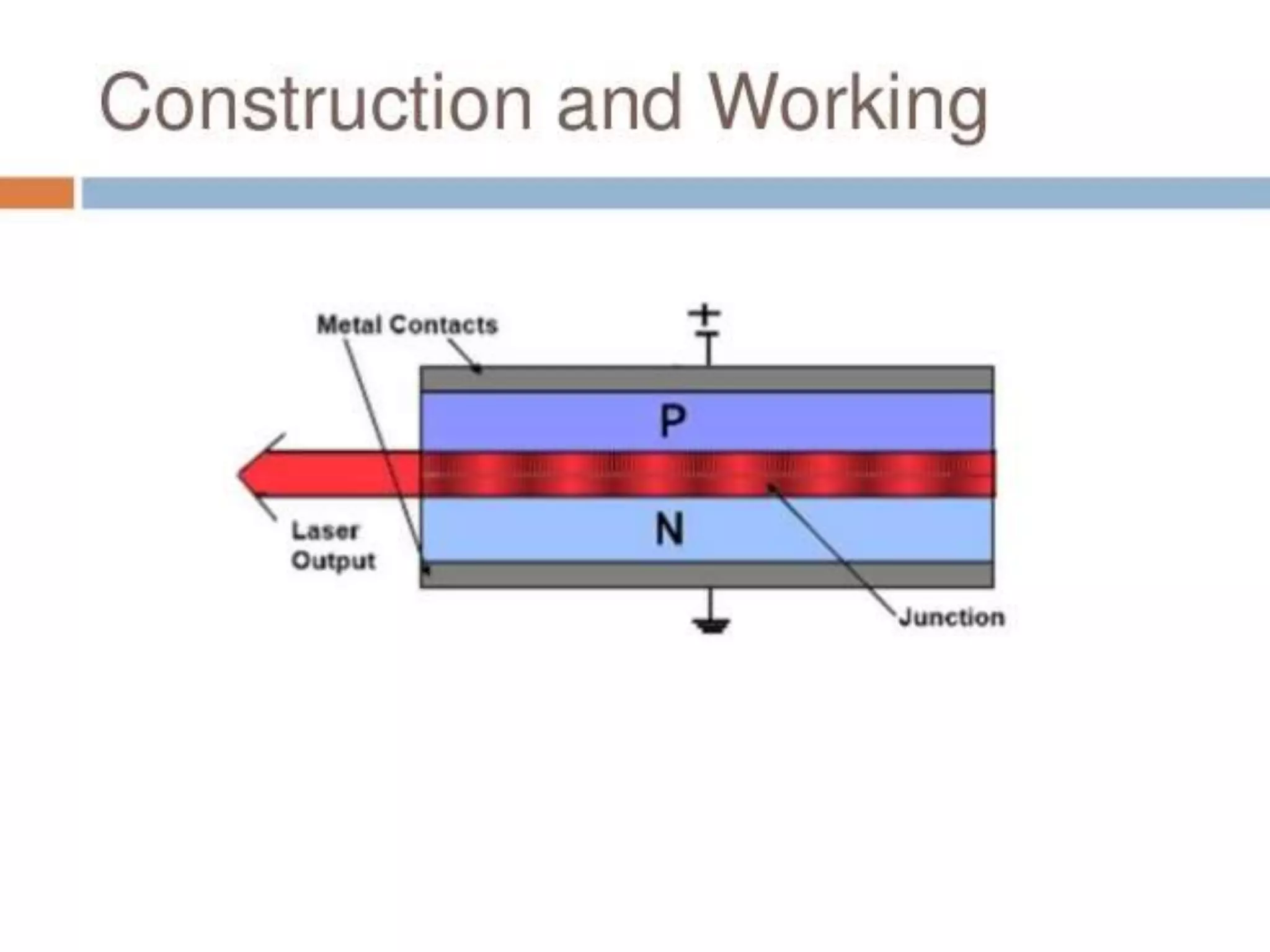
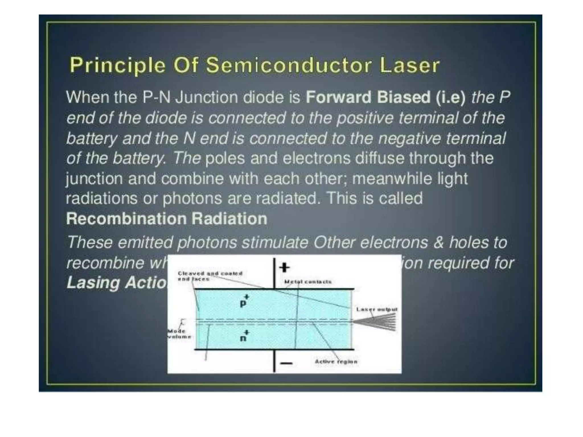
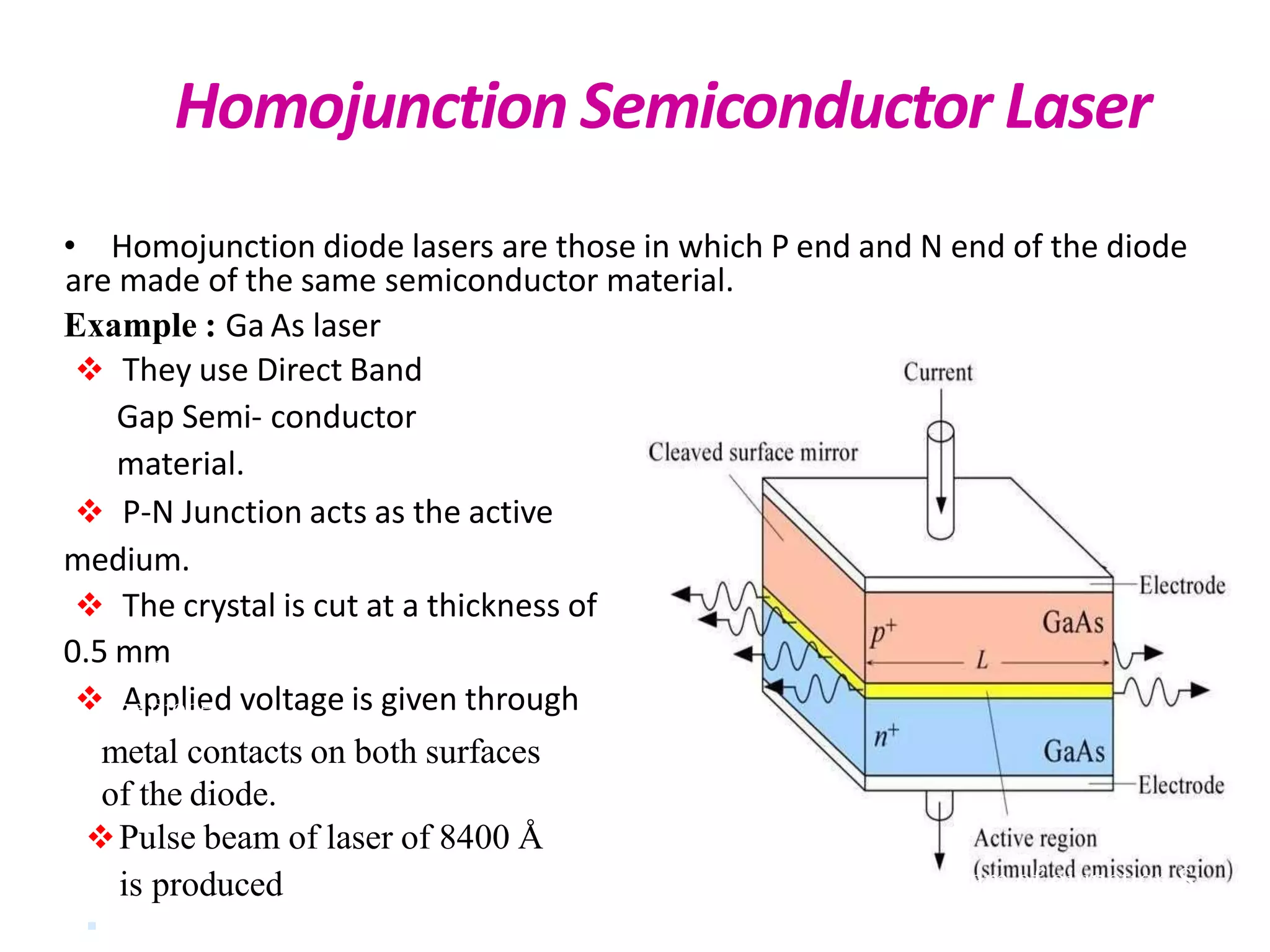
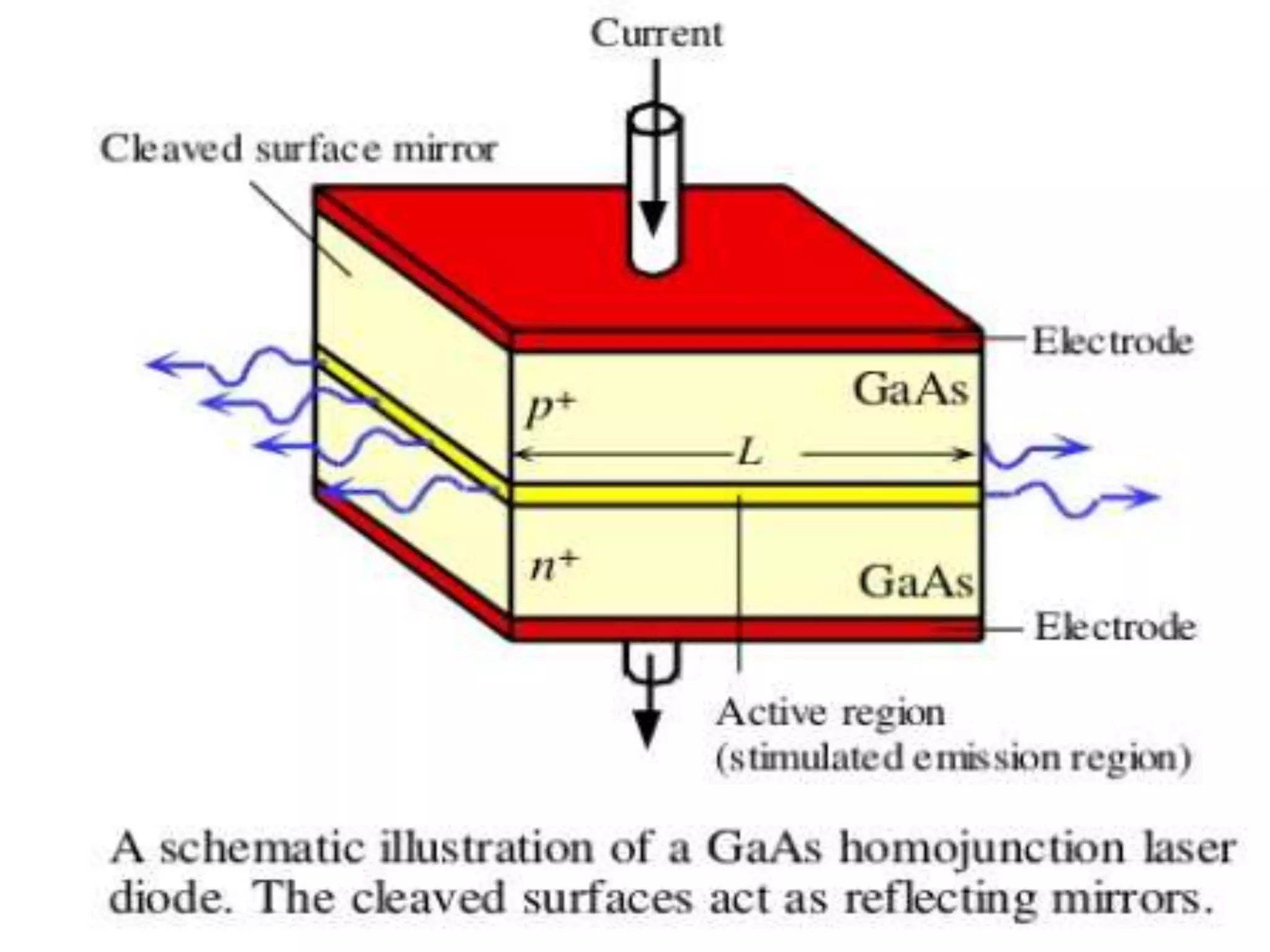
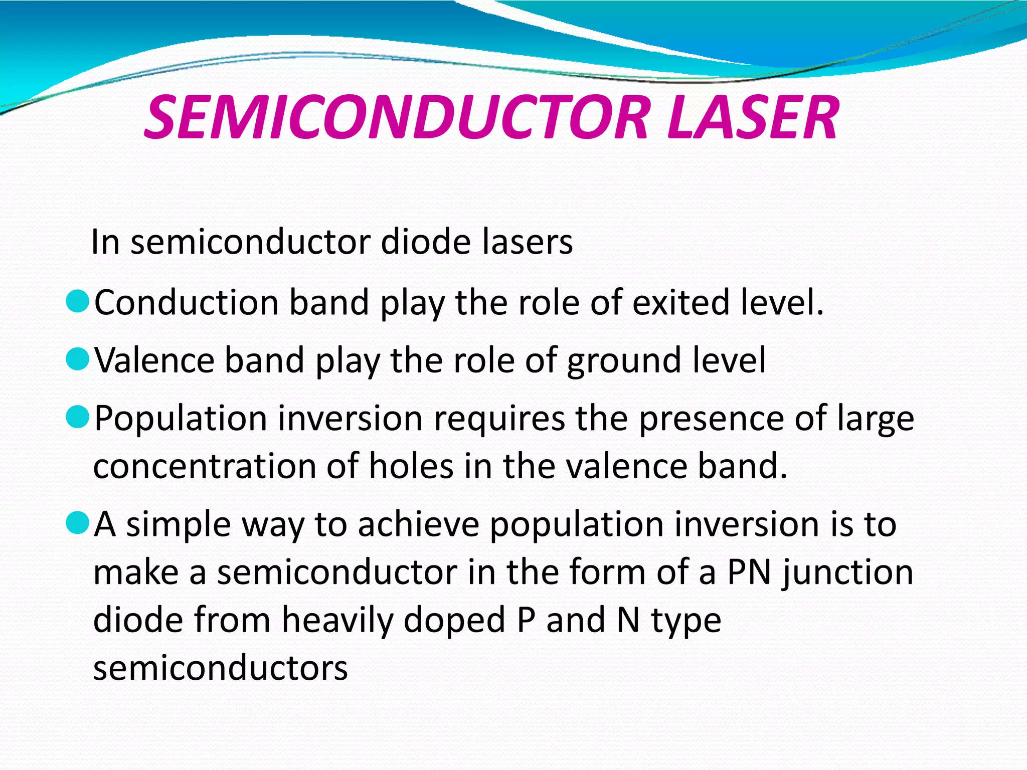
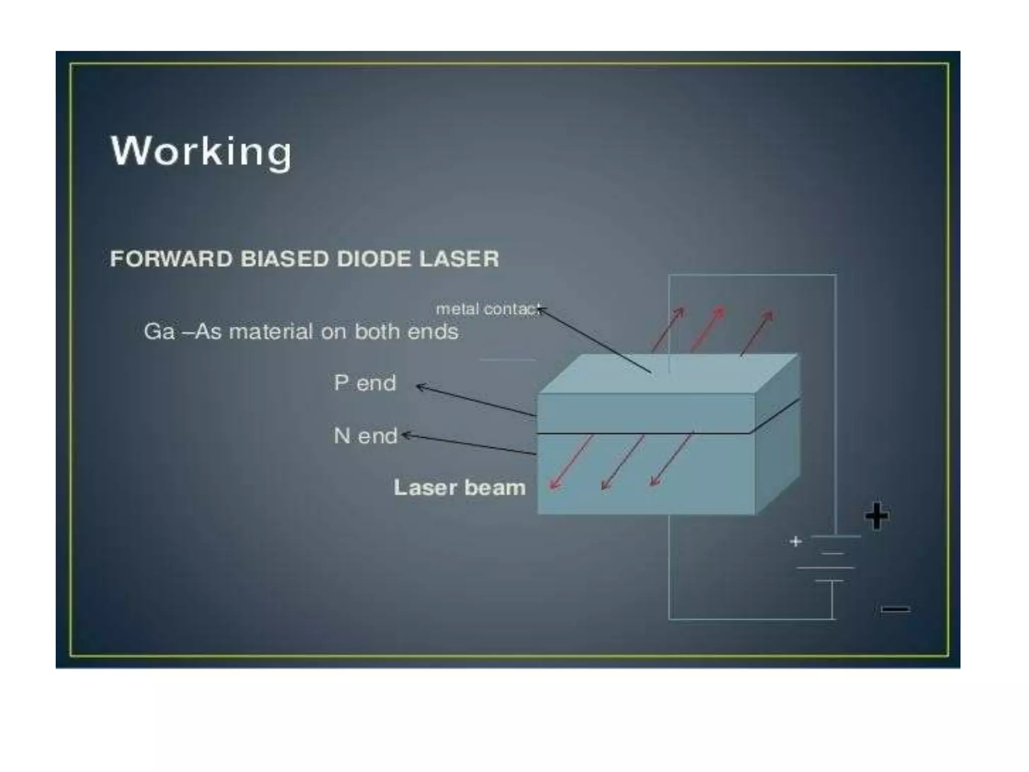
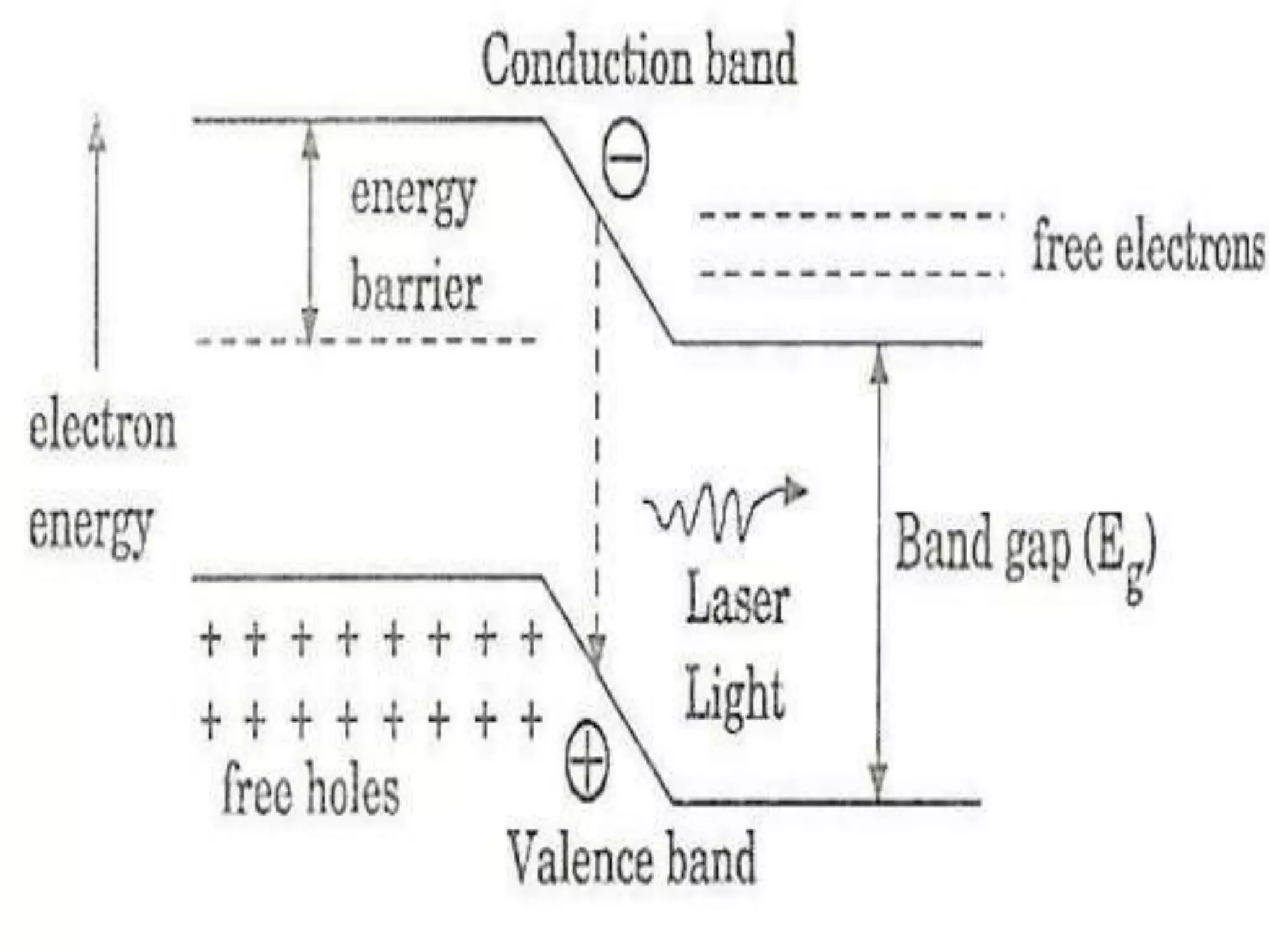
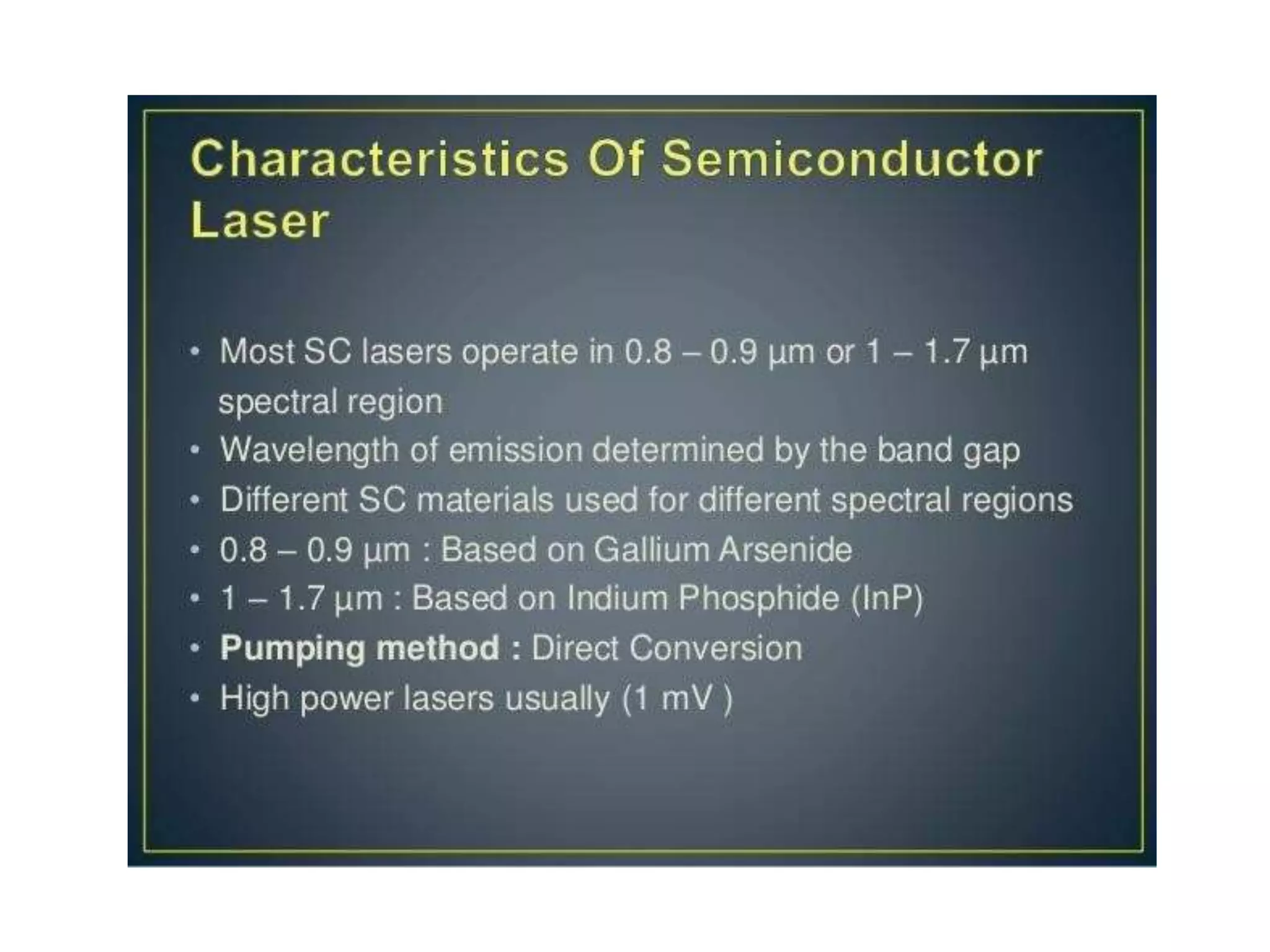
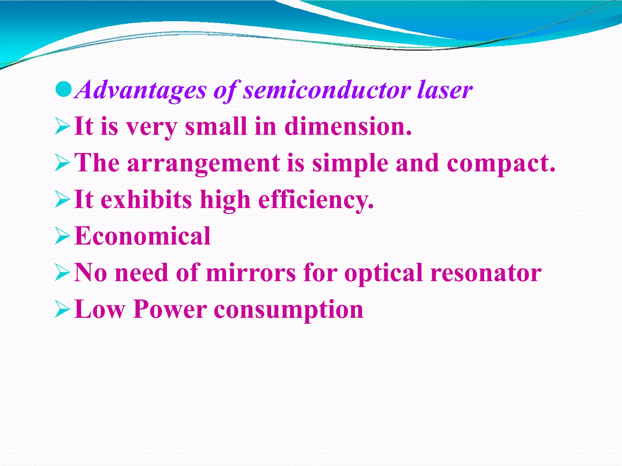
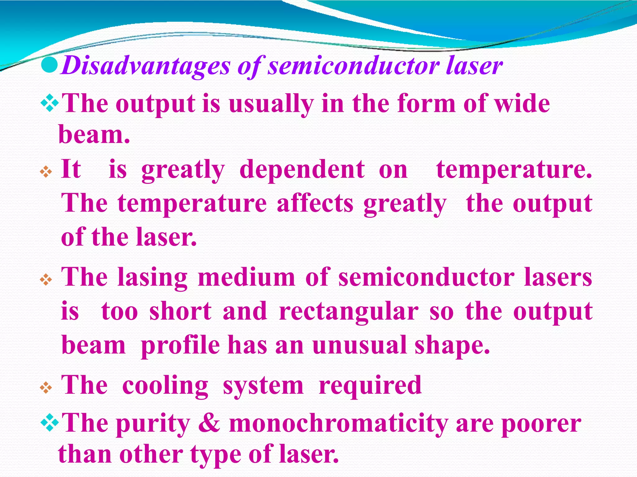
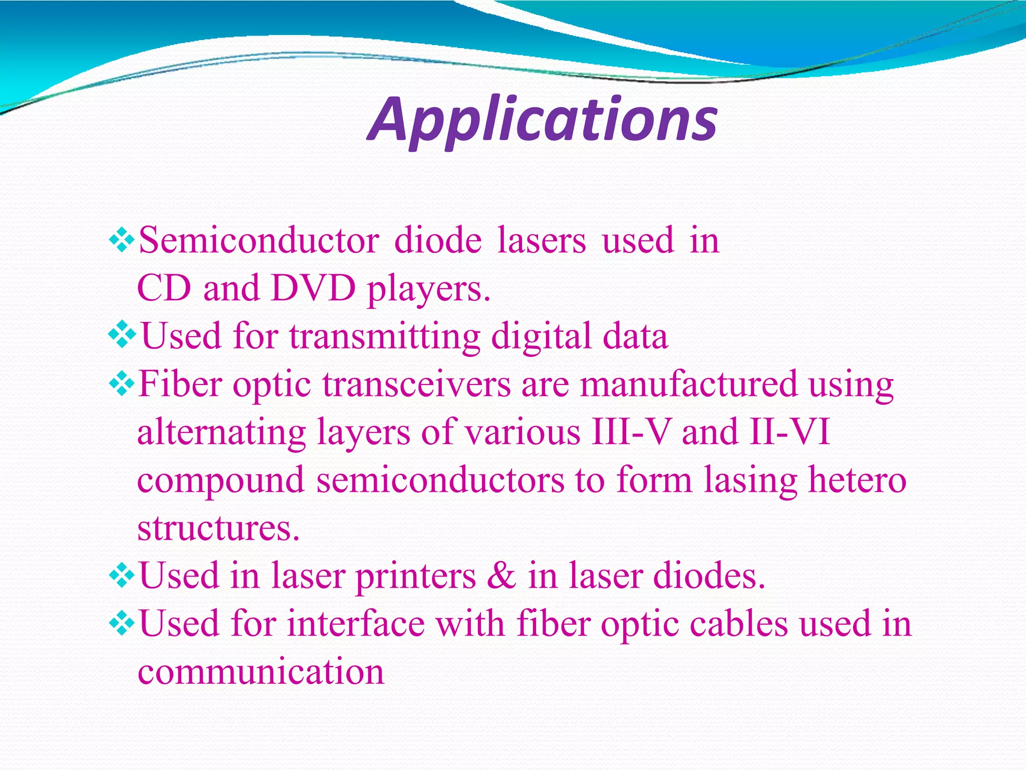
Semiconductor Diode Laser
 The semiconductor laser is very small in
size and appearance.
 It is similar to a transistor and has the
operation like LED but the output beam
has the characteristics of laser light.
 The material which often used in
semiconductor laser is the gallium
Arsenide, therefore semiconductor laser
is sometimes known as Gallium Arsenide
Laser.
 It is also called Injection Laser.
Components
• Active medium: PN Junction Diode
• Pumping Source: Forward Bias Voltage applied
(Direct Conversion)
• Optical Resonator: The polished ends of the
diode
Classification Of Semiconductor Laser
Semiconductor
Laser
Homojunction
Semiconductor Laser
Heterojunction
Semiconductor Laser
Double
Heterojunction
Semiconductor
Laser
Single
Heterojunction
Semiconductor Laser
Homojunction laser
It is simply a laser diode where the
active medium is a semiconductor
similar to that found in a light-
emitting diode. The most common
and practical type of laser diode is
formed from a p-n junction and
powered by injected electric current
Heterojunction laser
A hetero junction is the interface that
occurs between two laser or regions of
dissimilar crystalline semiconductors.
These semiconducting materials have
unequal band gaps as opposed to a homo
junction.
Homojunction Semiconductor Laser
• Homojunction diode lasers are those in which P end and N end of the diode
are made of the same semiconductor material.
Example : Ga As laser
 They use Direct Band
Gap Semi- conductor
material.
 P-N Junction acts as the active
medium.
 The crystal is cut at a thickness of
0.5 mm
 Applied voltage is given through
metal contacts on both surfaces of
the diode.
metal contacts on both surfaces
of the diode.
Pulse beam of laser of 8400 Å
is produced

Fig: Diagram of ojunction S
SEMICONDUCTOR LASER
In semiconductor diode lasers
⚫Conduction band play the role of exited level.
⚫Valence band play the role of ground level
⚫Population inversion requires the presence of large
concentration of holes in the valence band.
⚫A simple way to achieve population inversion is to
make a semiconductor in the form of a PN junction
diode from heavily doped P and N type
semiconductors
Pumping
⚫Direct conversion method is used.
⚫PRINCIPLE
P-TYPE CB P-N JUNCTION BAND STRUCTURE
HOLES JUNCTION
VB NO VOLTAGE N-TYPE
HOLE –ELECTRON RECOMBINATION
ELECTRONS
VOLTAGEAPPLIED
EMITED LIGHT
ENERGY LEVEL IN SEMICONDUTOR LASER
Pumping
Direct Conversion
⚫When PN junction diode is forward biased, the electrons
from ‘n’region and holes from ‘p’region recombine with
each other at the junction .
⚫During the recombination process light radiations
(photons) is released from certain specified direct band
gap semiconductors like Ga-As.
⚫This radiation is called recombination radiation and the
corresponding energy is called activation energy.
Construction of Ga - As LASER
⚫The galliumArsenide laser is designed in such a way
that a piece of N-type Gallium Arsenide material is
taken and a layer of natural gallium aluminum
arsenide material is pasted, The third layer of p-type
gallium arsenide material is pasted over that.
⚫The two ends of length wise are fully polished in
order to amplify the light by cross reflection. Here
one ends is partially polished from where we get the
laser beam.
CONSTUCTION
METALLIC LAYER
GaAs CONTACT LAYER
GaAl As BARRIER LAYER LASERBEAM
Ga As CONTACT LAYER
Ga Al As BARRIER LAYER
Ga As CONTACT LAYER
+ -
GALLIUM ARSENIDE LASER
Working of Ga – As LASER
⚫When the forward bias is applied to the metallic layer through
contact points. The electric field is produced. This electric field
causes the electrons to move from lower band of energy
towards high band of energy level.
⚫Population inversion take place at the higher band of energy
level and when the electrons falls back at the lower energy
band, it emits light, through the polished end of the laser.
⚫ Cross reflection of the light take place which multiplies
strength of laser beam.At the end strong beam of laser comes
out through the partially polished end.
Pictorial View
⚫
⚫ No biasing Biasing
⚫When p-n junction diode is forward biased, then there will be
injection of electrons into the conduction band along n-side
and production of more holes in valence band along p-side of
the junction. Thus, there will be more number of electrons in
conduction band comparable to valence band, so population
inversion is achieved.
⚫Therefore, when the electrons and holes are injected into the
junction region from opposite sides with forward biasing, then
population inversion is achieved between levels near the bottom
of the conduction band and empty levels near the top of the
valence band.
Achievement of population inversion
Achievement of laser
⚫When electrons recombine with the holes in junction region,
then there will be release of energy in the form of photons. This
release of energy in the form of photons happen only in special
types of semiconductors like GalliumArsenide (GaAs).
⚫Otherwise in semiconductors like silicon and germanium,
whenever holes and electrons recombine, energy is released in
the form of heat, thus Si and Ge can not be used for the
production of laser.
⚫The spontaneously emitted photon during recombination in the
junction region of Ga As will trigger laser action near the
junction diode. The photons emitted have a wavelength from
8200 Å to 9000 Å in the infrared region.
Heterojunction Semiconductor Laser
Heterojunction Semiconductor lasers are those in which P end is made of one type of
semiconductor material and the N end is made of another type of semiconductor
material
Example : GaAlAs diode laser
 Use Direct Band gap
Semiconductor
Consist of five layers namely
 GaAs – p type
 GaAlAs – p type
 GaAs – p type (Active Medium)
 GaAIAs – n type
 GaAs – n type
The end faces of the third layer is highly polished and perfectly parallel to each
other to reflect the laser beam; one end is partially polished to release the
continuous beam
Energy Level Diagram : Heterojunction
Fig : Energy level Diagram of
Heterojunction Semiconductor Laser
Characteristics
 Type: It is a solid state semiconductor laser.
 Active medium: A PN junction diode made from
single crystal of gallium arsenide is used as an
active medium.
 Pumping method: The direct conversion
method is used for pumping action
 Power output: The power output from this laser
is 1mW.
 Nature of output: The nature of output is
continuous wave or pulsed output.
⚫Advantages of semiconductor laser
It is very small in dimension.
The arrangement is simple and compact.
It exhibits high efficiency.
Economical
No need of mirrors for optical resonator
Low Power consumption
⚫Disadvantages of semiconductor laser
The output is usually in the form of wide
beam.
 It is greatly dependent on temperature.
The temperature affects greatly the output
of the laser.
 The lasing medium of semiconductor lasers
is too short and rectangular so the output
beam profile has an unusual shape.
 The cooling system required
The purity & monochromaticity are poorer
than other type of laser.
Applications
Semiconductor diode lasers used in
CD and DVD players.
Used for transmitting digital data
Fiber optic transceivers are manufactured using
alternating layers of various III-V and II-VI
compound semiconductors to form lasing hetero
structures.
Used in laser printers & in laser diodes.
Used for interface with fiber optic cables used in
communication

semiconductor diode laser.pptx

  • 3.
    Semiconductor Diode Laser The semiconductor laser is very small in size and appearance.  It is similar to a transistor and has the operation like LED but the output beam has the characteristics of laser light.  The material which often used in semiconductor laser is the gallium Arsenide, therefore semiconductor laser is sometimes known as Gallium Arsenide Laser.  It is also called Injection Laser.
  • 7.
    Components • Active medium:PN Junction Diode • Pumping Source: Forward Bias Voltage applied (Direct Conversion) • Optical Resonator: The polished ends of the diode
  • 9.
    Classification Of SemiconductorLaser Semiconductor Laser Homojunction Semiconductor Laser Heterojunction Semiconductor Laser Double Heterojunction Semiconductor Laser Single Heterojunction Semiconductor Laser
  • 10.
    Homojunction laser It issimply a laser diode where the active medium is a semiconductor similar to that found in a light- emitting diode. The most common and practical type of laser diode is formed from a p-n junction and powered by injected electric current
  • 11.
    Heterojunction laser A heterojunction is the interface that occurs between two laser or regions of dissimilar crystalline semiconductors. These semiconducting materials have unequal band gaps as opposed to a homo junction.
  • 12.
    Homojunction Semiconductor Laser •Homojunction diode lasers are those in which P end and N end of the diode are made of the same semiconductor material. Example : Ga As laser  They use Direct Band Gap Semi- conductor material.  P-N Junction acts as the active medium.  The crystal is cut at a thickness of 0.5 mm  Applied voltage is given through metal contacts on both surfaces of the diode. metal contacts on both surfaces of the diode. Pulse beam of laser of 8400 Å is produced  Fig: Diagram of ojunction S
  • 14.
    SEMICONDUCTOR LASER In semiconductordiode lasers ⚫Conduction band play the role of exited level. ⚫Valence band play the role of ground level ⚫Population inversion requires the presence of large concentration of holes in the valence band. ⚫A simple way to achieve population inversion is to make a semiconductor in the form of a PN junction diode from heavily doped P and N type semiconductors
  • 18.
    Pumping ⚫Direct conversion methodis used. ⚫PRINCIPLE P-TYPE CB P-N JUNCTION BAND STRUCTURE HOLES JUNCTION VB NO VOLTAGE N-TYPE HOLE –ELECTRON RECOMBINATION ELECTRONS VOLTAGEAPPLIED EMITED LIGHT ENERGY LEVEL IN SEMICONDUTOR LASER
  • 19.
    Pumping Direct Conversion ⚫When PNjunction diode is forward biased, the electrons from ‘n’region and holes from ‘p’region recombine with each other at the junction . ⚫During the recombination process light radiations (photons) is released from certain specified direct band gap semiconductors like Ga-As. ⚫This radiation is called recombination radiation and the corresponding energy is called activation energy.
  • 20.
    Construction of Ga- As LASER ⚫The galliumArsenide laser is designed in such a way that a piece of N-type Gallium Arsenide material is taken and a layer of natural gallium aluminum arsenide material is pasted, The third layer of p-type gallium arsenide material is pasted over that. ⚫The two ends of length wise are fully polished in order to amplify the light by cross reflection. Here one ends is partially polished from where we get the laser beam.
  • 21.
    CONSTUCTION METALLIC LAYER GaAs CONTACTLAYER GaAl As BARRIER LAYER LASERBEAM Ga As CONTACT LAYER Ga Al As BARRIER LAYER Ga As CONTACT LAYER + - GALLIUM ARSENIDE LASER
  • 22.
    Working of Ga– As LASER ⚫When the forward bias is applied to the metallic layer through contact points. The electric field is produced. This electric field causes the electrons to move from lower band of energy towards high band of energy level. ⚫Population inversion take place at the higher band of energy level and when the electrons falls back at the lower energy band, it emits light, through the polished end of the laser. ⚫ Cross reflection of the light take place which multiplies strength of laser beam.At the end strong beam of laser comes out through the partially polished end.
  • 23.
  • 24.
    ⚫When p-n junctiondiode is forward biased, then there will be injection of electrons into the conduction band along n-side and production of more holes in valence band along p-side of the junction. Thus, there will be more number of electrons in conduction band comparable to valence band, so population inversion is achieved. ⚫Therefore, when the electrons and holes are injected into the junction region from opposite sides with forward biasing, then population inversion is achieved between levels near the bottom of the conduction band and empty levels near the top of the valence band. Achievement of population inversion
  • 25.
    Achievement of laser ⚫Whenelectrons recombine with the holes in junction region, then there will be release of energy in the form of photons. This release of energy in the form of photons happen only in special types of semiconductors like GalliumArsenide (GaAs). ⚫Otherwise in semiconductors like silicon and germanium, whenever holes and electrons recombine, energy is released in the form of heat, thus Si and Ge can not be used for the production of laser. ⚫The spontaneously emitted photon during recombination in the junction region of Ga As will trigger laser action near the junction diode. The photons emitted have a wavelength from 8200 Å to 9000 Å in the infrared region.
  • 26.
    Heterojunction Semiconductor Laser HeterojunctionSemiconductor lasers are those in which P end is made of one type of semiconductor material and the N end is made of another type of semiconductor material Example : GaAlAs diode laser  Use Direct Band gap Semiconductor Consist of five layers namely  GaAs – p type  GaAlAs – p type  GaAs – p type (Active Medium)  GaAIAs – n type  GaAs – n type The end faces of the third layer is highly polished and perfectly parallel to each other to reflect the laser beam; one end is partially polished to release the continuous beam
  • 27.
    Energy Level Diagram: Heterojunction Fig : Energy level Diagram of Heterojunction Semiconductor Laser
  • 30.
    Characteristics  Type: Itis a solid state semiconductor laser.  Active medium: A PN junction diode made from single crystal of gallium arsenide is used as an active medium.  Pumping method: The direct conversion method is used for pumping action  Power output: The power output from this laser is 1mW.  Nature of output: The nature of output is continuous wave or pulsed output.
  • 33.
    ⚫Advantages of semiconductorlaser It is very small in dimension. The arrangement is simple and compact. It exhibits high efficiency. Economical No need of mirrors for optical resonator Low Power consumption
  • 34.
    ⚫Disadvantages of semiconductorlaser The output is usually in the form of wide beam.  It is greatly dependent on temperature. The temperature affects greatly the output of the laser.  The lasing medium of semiconductor lasers is too short and rectangular so the output beam profile has an unusual shape.  The cooling system required The purity & monochromaticity are poorer than other type of laser.
  • 35.
    Applications Semiconductor diode lasersused in CD and DVD players. Used for transmitting digital data Fiber optic transceivers are manufactured using alternating layers of various III-V and II-VI compound semiconductors to form lasing hetero structures. Used in laser printers & in laser diodes. Used for interface with fiber optic cables used in communication