![Atlys Spartan-6 overview
Figure 1: Atlys Spartan-6 XC6SLX45 [1]](https://image.slidesharecdn.com/fpgatutorialen-151229042010/85/FPGA-FIR-filter-implementation-Audio-signal-processing-3-320.jpg)
![Atlys Spartan-6 overview
FPGA features
Resources Size
Slices (6-input LUT and 8 flip-flops) 6822
Block RAM 2.1 Mbits
Clock management tiles (2 DCM and 1 PLL) 4
DSP slices 58
Clock speeds 500Mhz+
Table 1: Spartan-6 (XC6SLX45) features [1]
4](https://image.slidesharecdn.com/fpgatutorialen-151229042010/85/FPGA-FIR-filter-implementation-Audio-signal-processing-4-320.jpg)
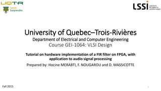
![Atlys Spartan-6 overview
Audio circuit features (LM4550)
Figure 2: LM4550-FPGA interface [1]
Parameter Value
Codec AC-97
Headphone out Stereo
Line out Stereo
Line in Stereo
Mic in Mono
Sampling frequency 48 Khz
Word-length 18 bits
Table 2: LM4550 features [1]
5](https://image.slidesharecdn.com/fpgatutorialen-151229042010/85/FPGA-FIR-filter-implementation-Audio-signal-processing-5-320.jpg)


![References
[1] https://reference.digilentinc.com/_media/atlys:atlys:atlys_rm.pdf
[2] https://reference.digilentinc.com/_media/atlys:atlys:atlys_sch.pdf
[3] https://eewiki.net/display/LOGIC/AC'97+Codec+Hardware+Driver+Example
18](https://image.slidesharecdn.com/fpgatutorialen-151229042010/85/FPGA-FIR-filter-implementation-Audio-signal-processing-18-320.jpg)

The document is a tutorial for implementing a FIR filter on an FPGA, specifically using the Atlys Spartan-6 and applicable to audio signal processing. It covers skills such as hardware modeling with VHDL, design verification, and FPGA programming, along with details on filtering system architecture. Additionally, it includes step-by-step instructions for filter design, integration, and testing with audio signals.