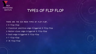
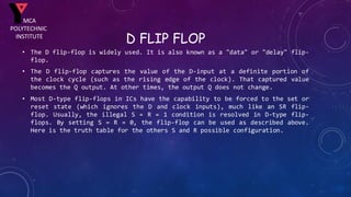
1. The document discusses different types of flip-flops including D flip-flops, T flip-flops, and JK flip-flops.
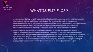
2. A flip-flop is a circuit that has two stable states and is used to store digital information. It is the basic storage element in sequential logic.
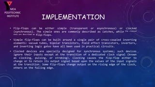
3. The document provides details on the operation and implementation of different types of flip-flops such as how a D flip-flop stores input data on the rising edge of a clock signal.


![SEQUENTIAL CIRCUITS [Flip-flops and Latches]](https://cdn.slidesharecdn.com/ss_thumbnails/sequentialcircuits-211217082412-thumbnail.jpg?width=640&height=640&fit=bounds)


![Flip_flops_in_digital_electronics[1].pptx](https://cdn.slidesharecdn.com/ss_thumbnails/flipflopsindigitalelectronics1-250805201548-623d4f88-thumbnail.jpg?width=640&height=640&fit=bounds)
![Flip_flops_in_digital_electronics[1].pptx](https://cdn.slidesharecdn.com/ss_thumbnails/flipflopsindigitalelectronics1-250805201909-5c7c72ae-thumbnail.jpg?width=640&height=640&fit=bounds)