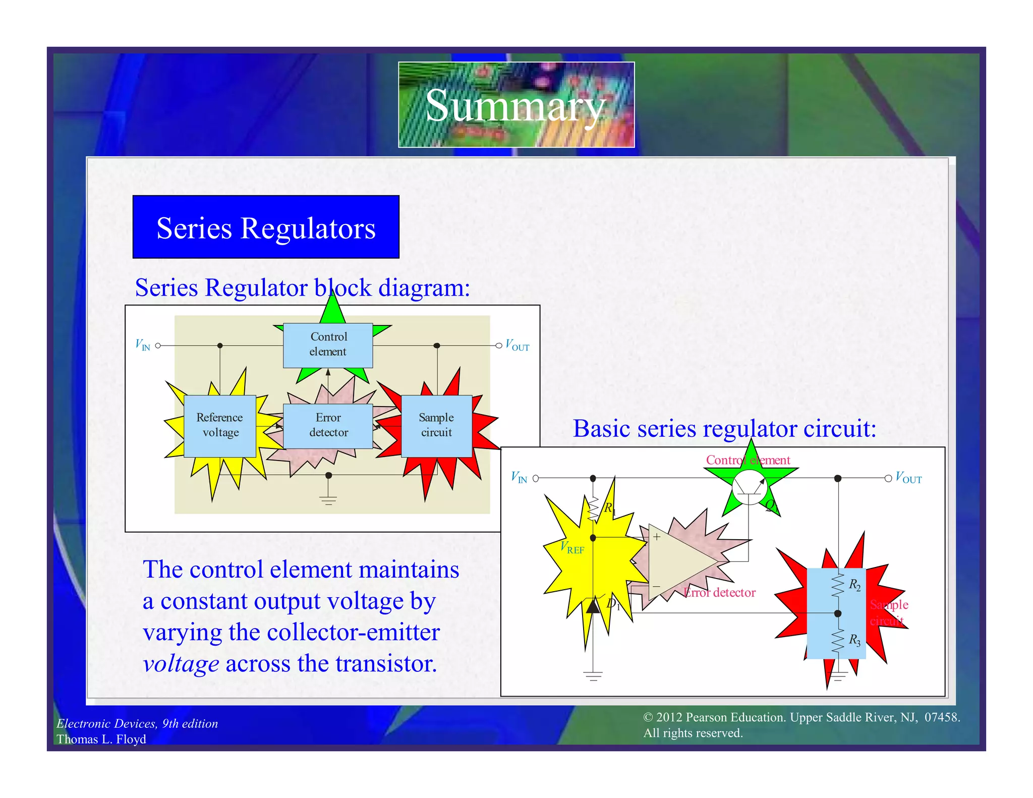
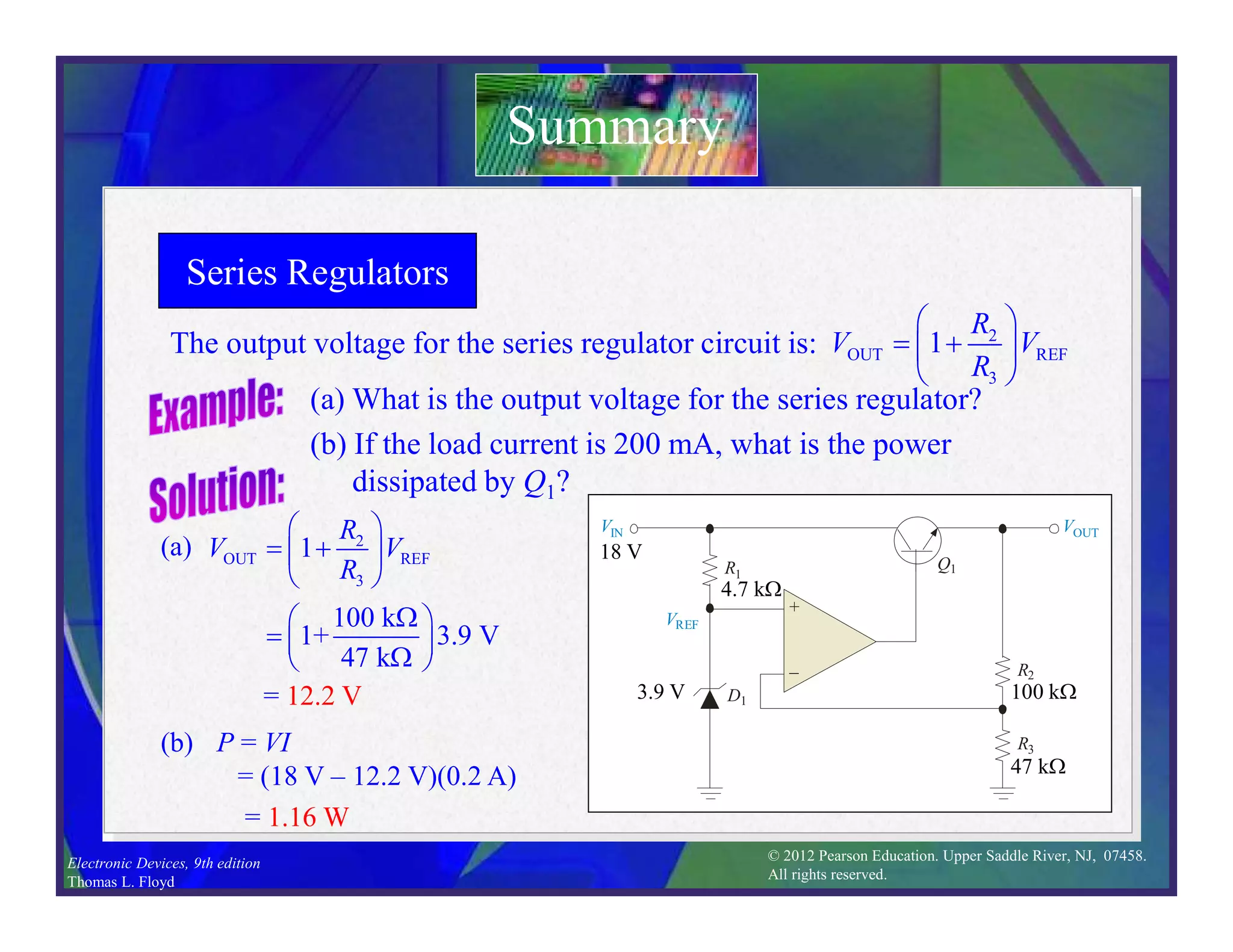
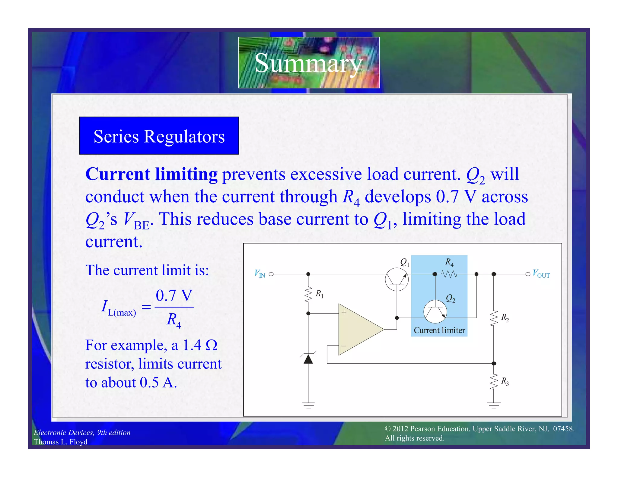
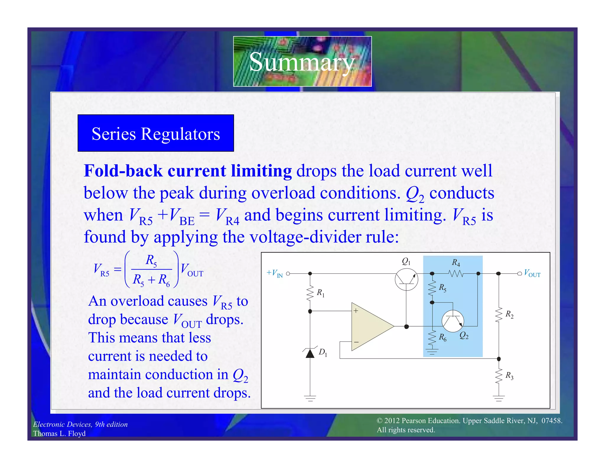
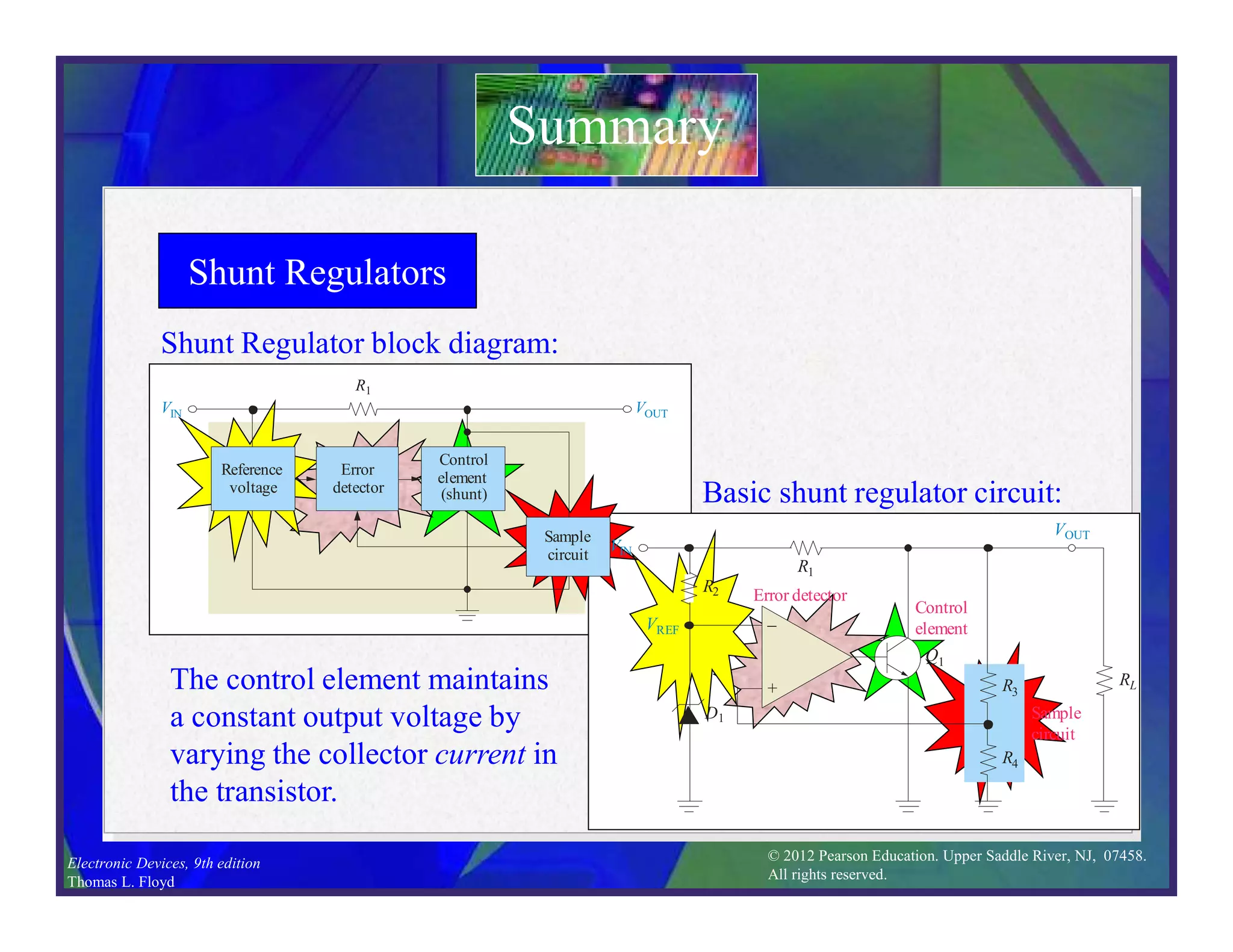
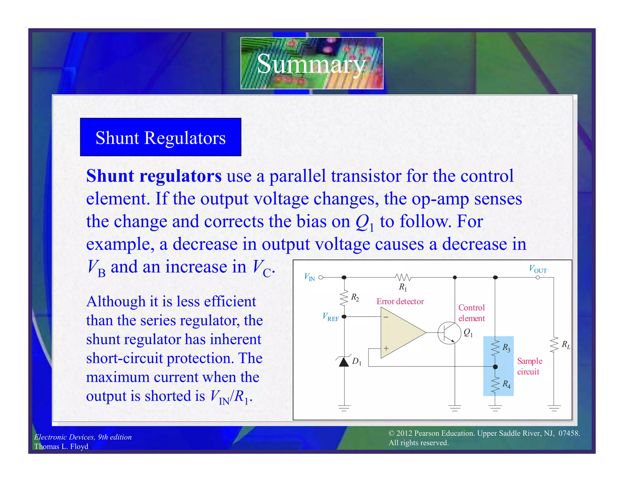
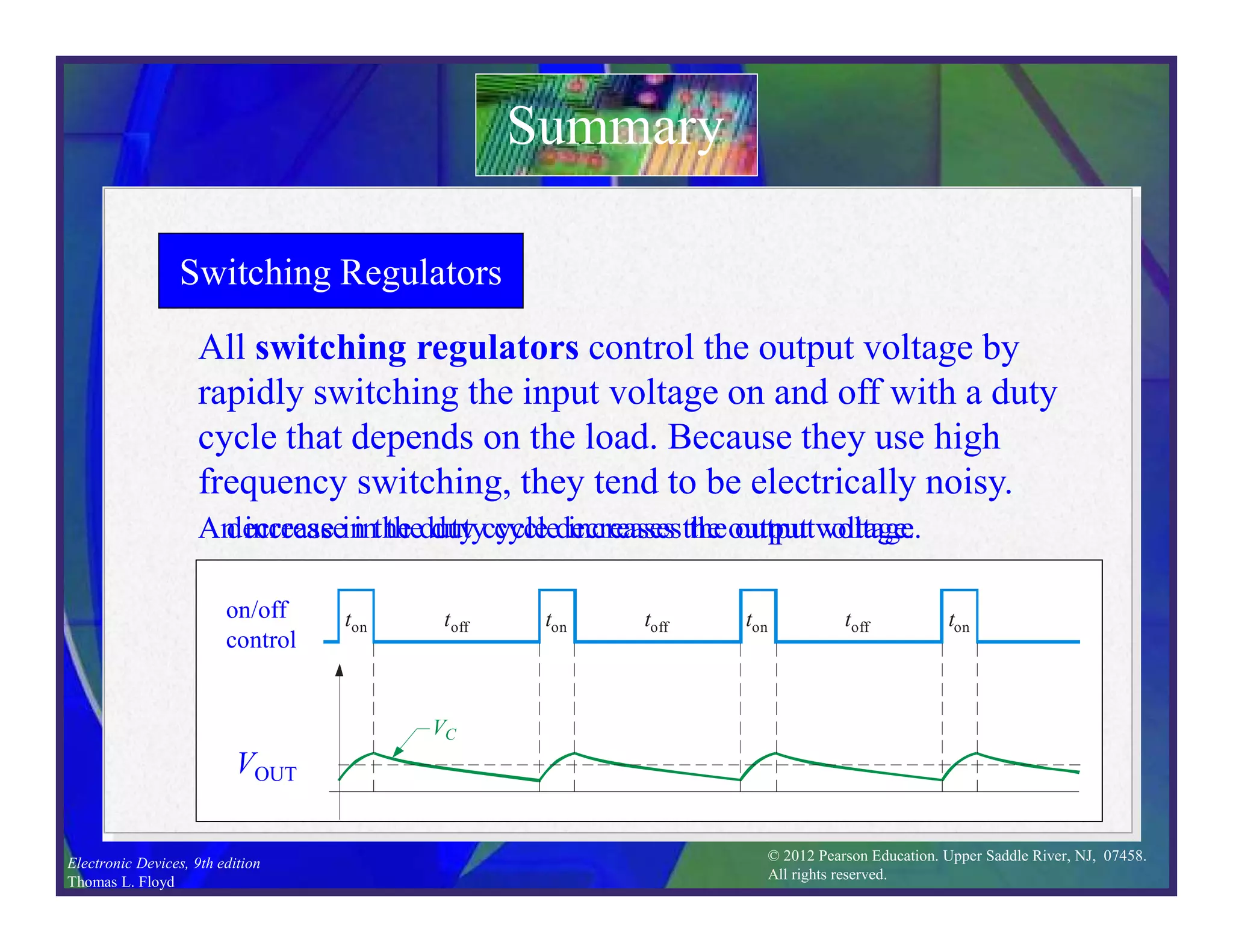
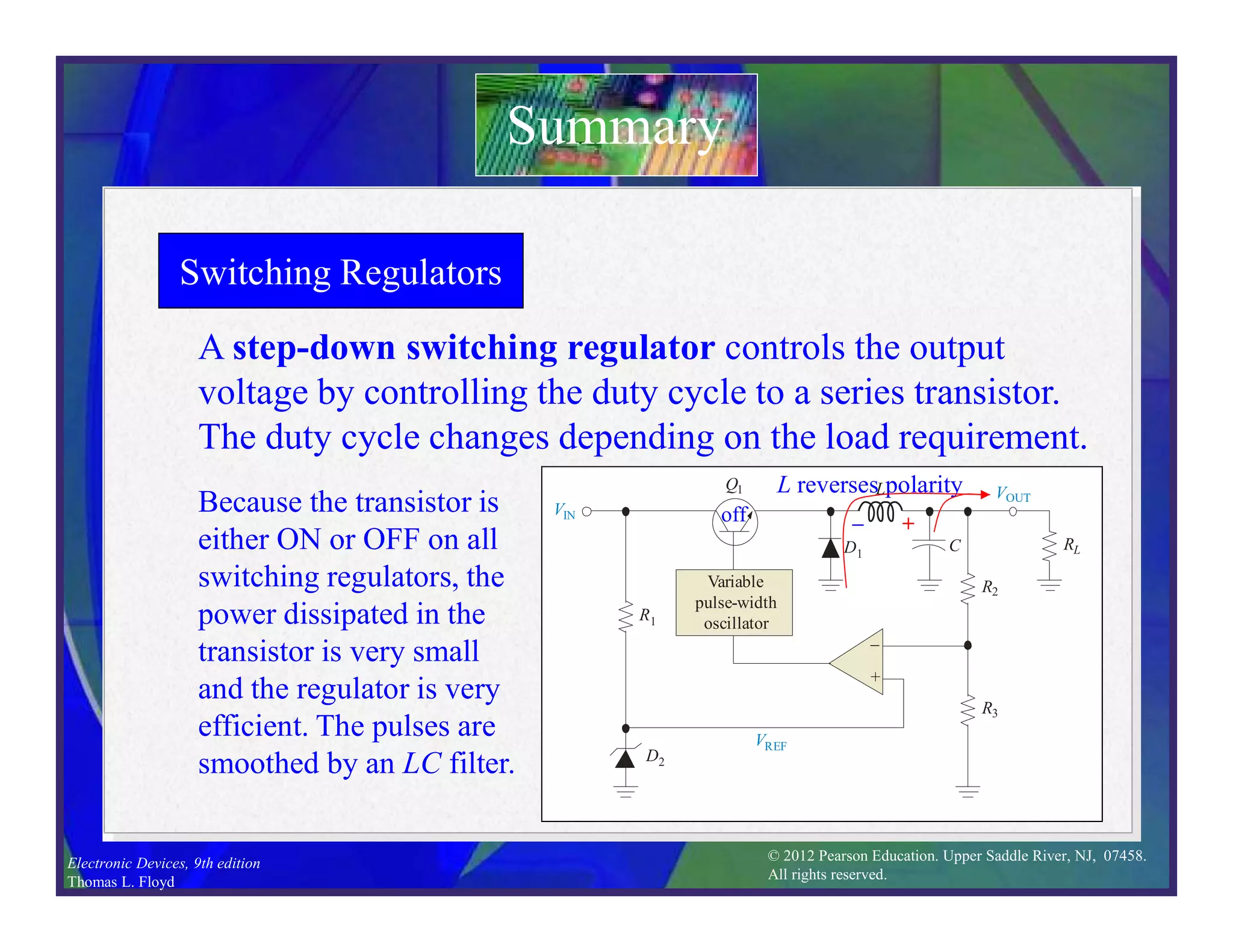
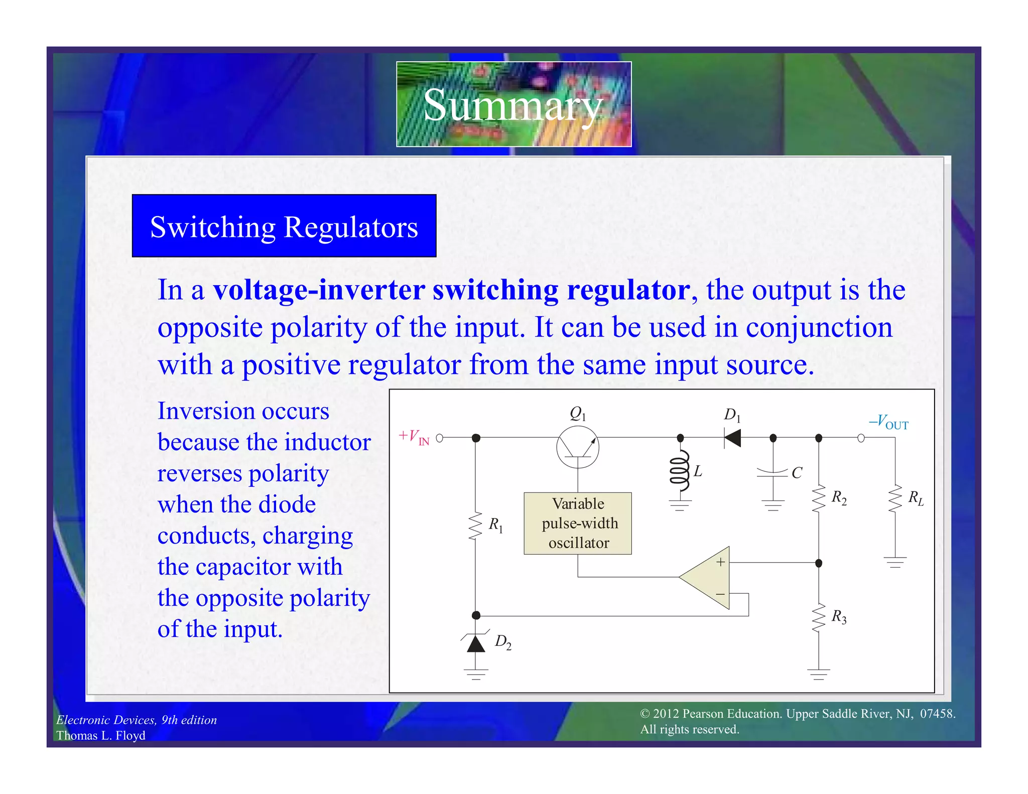
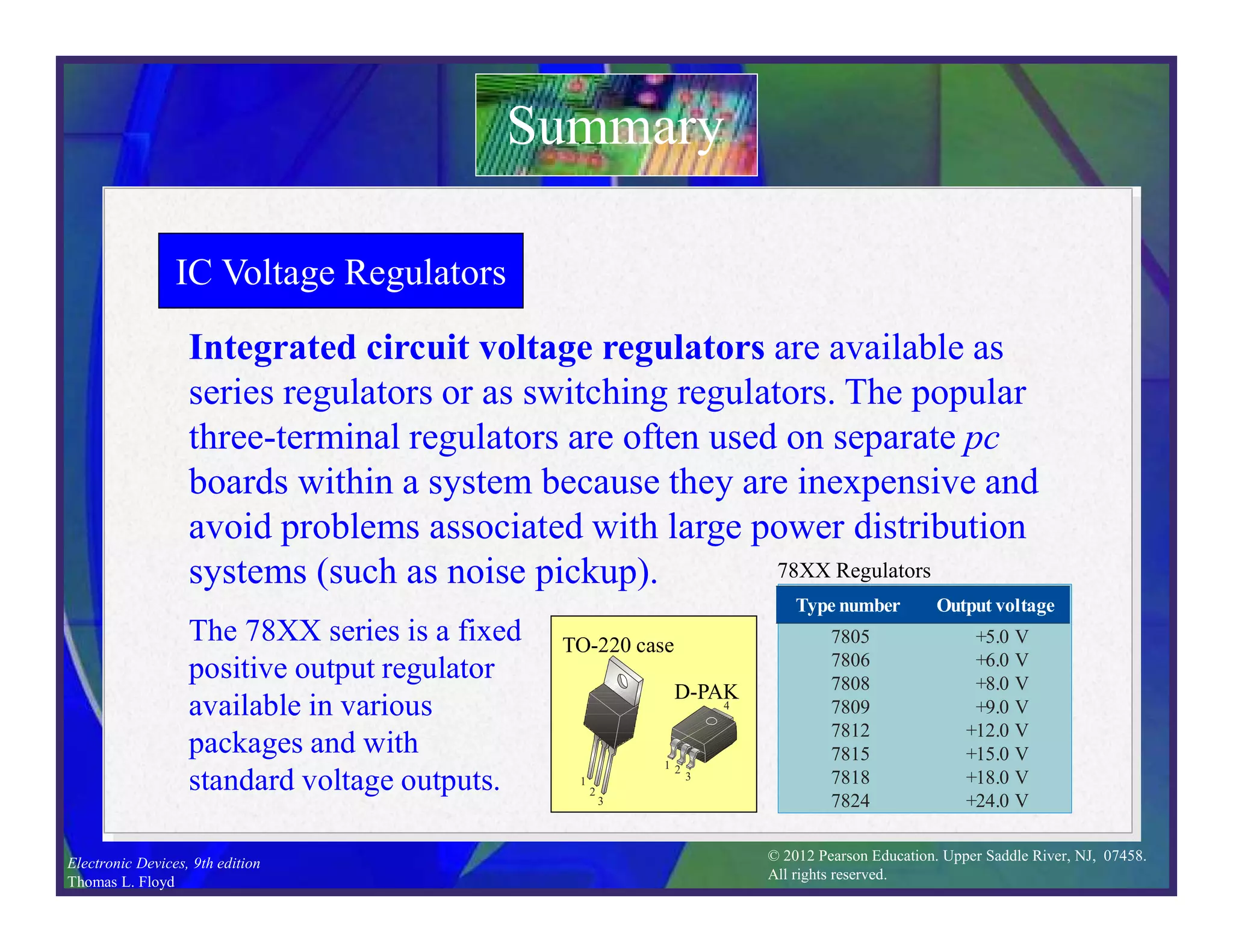
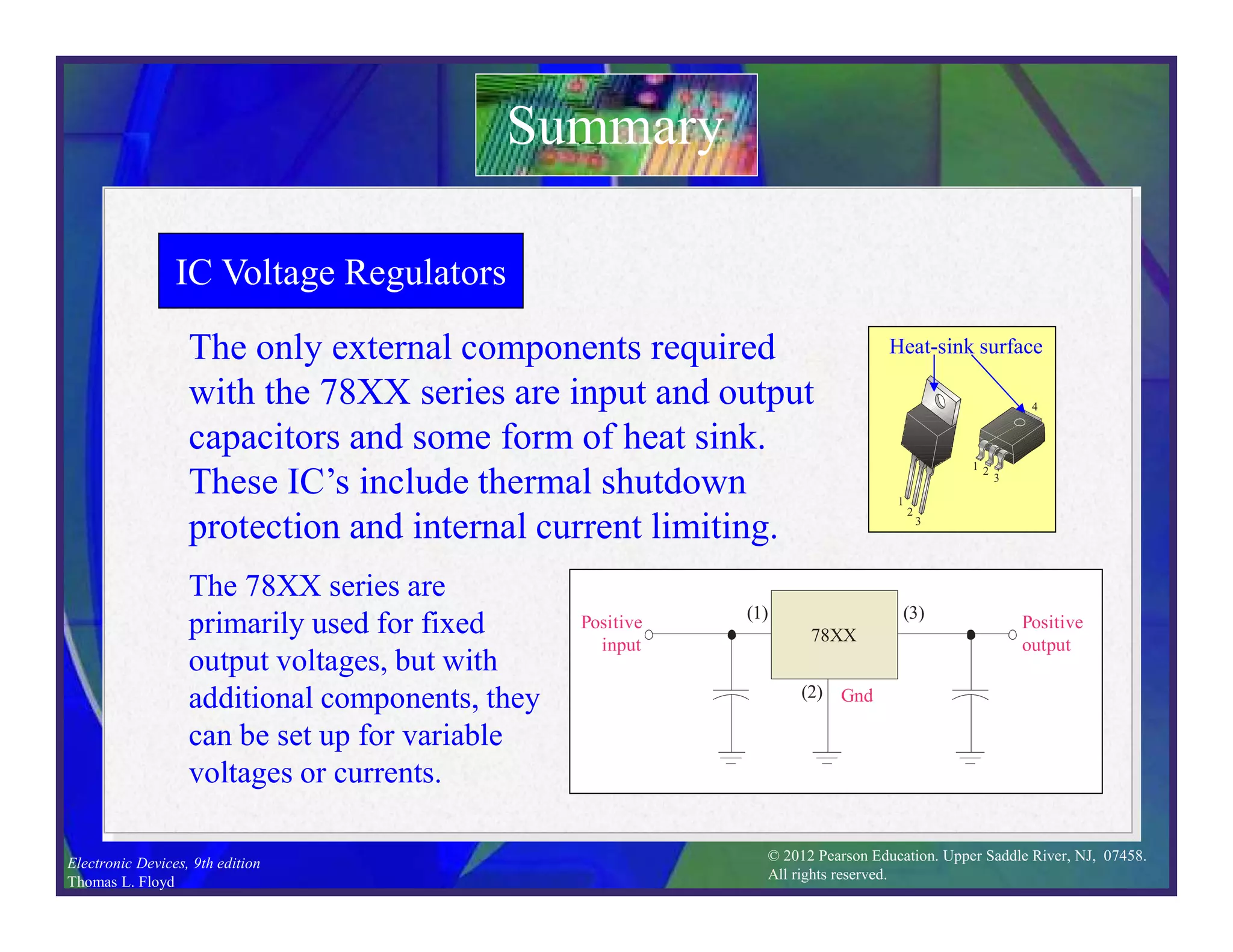
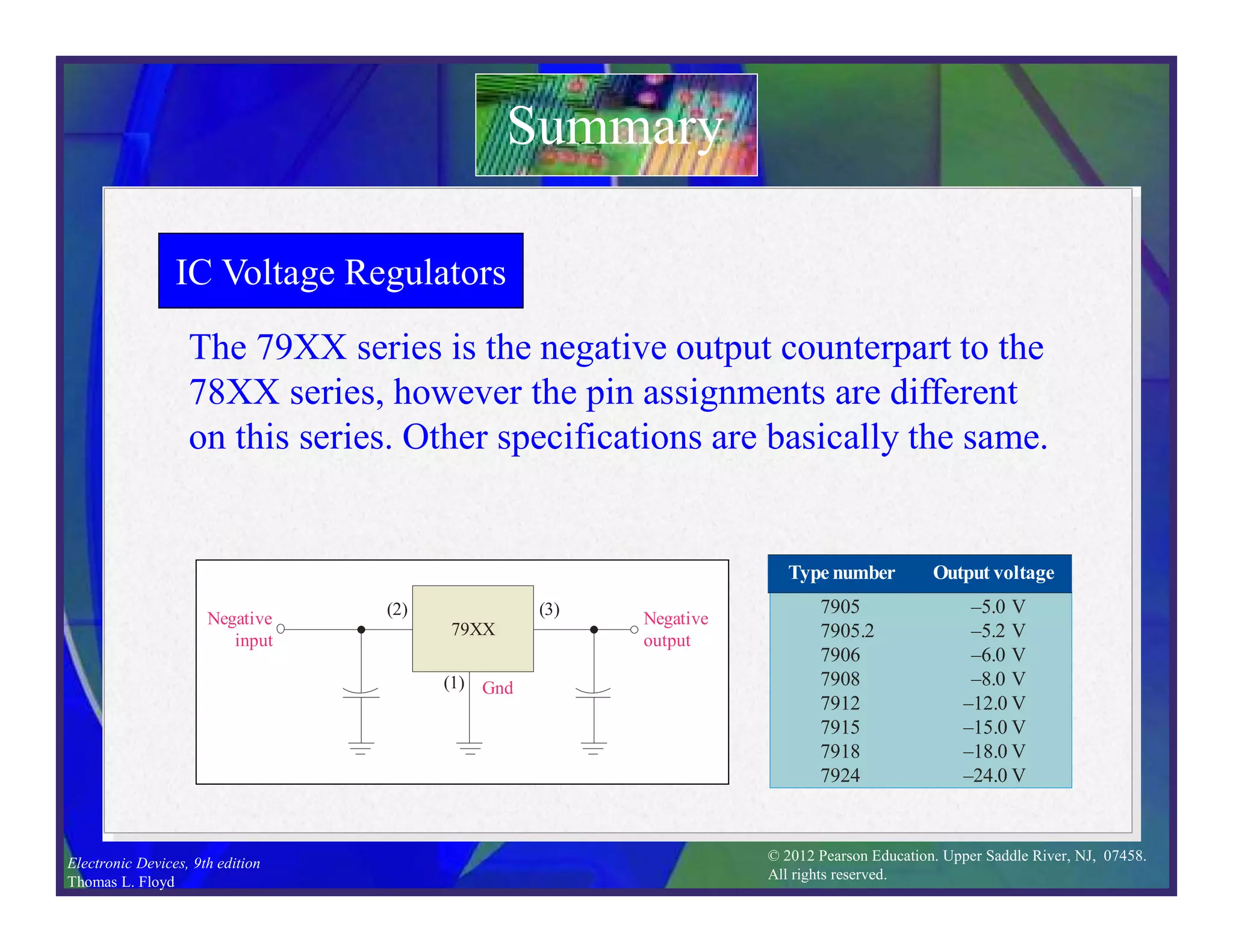
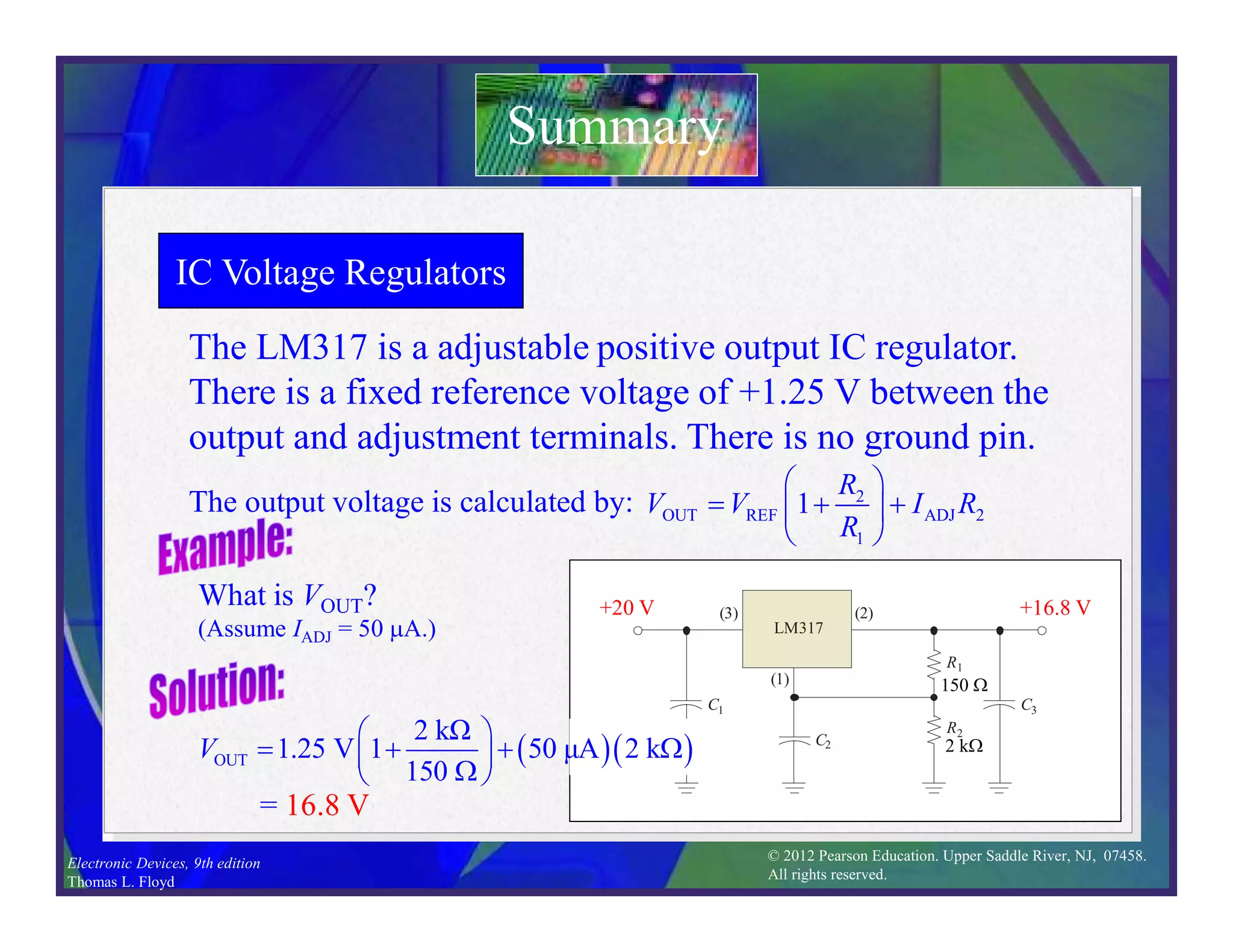
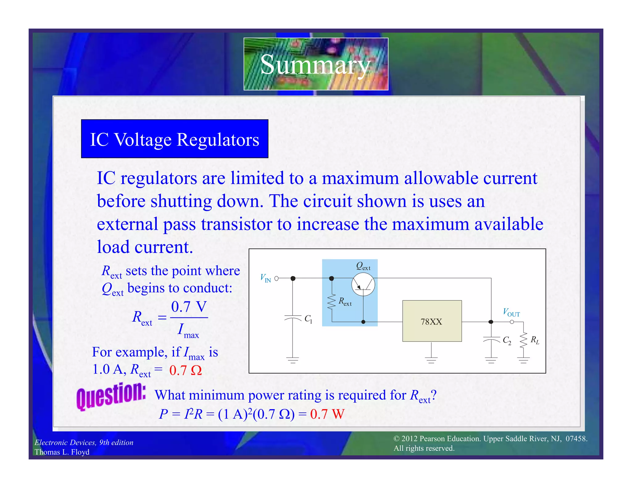
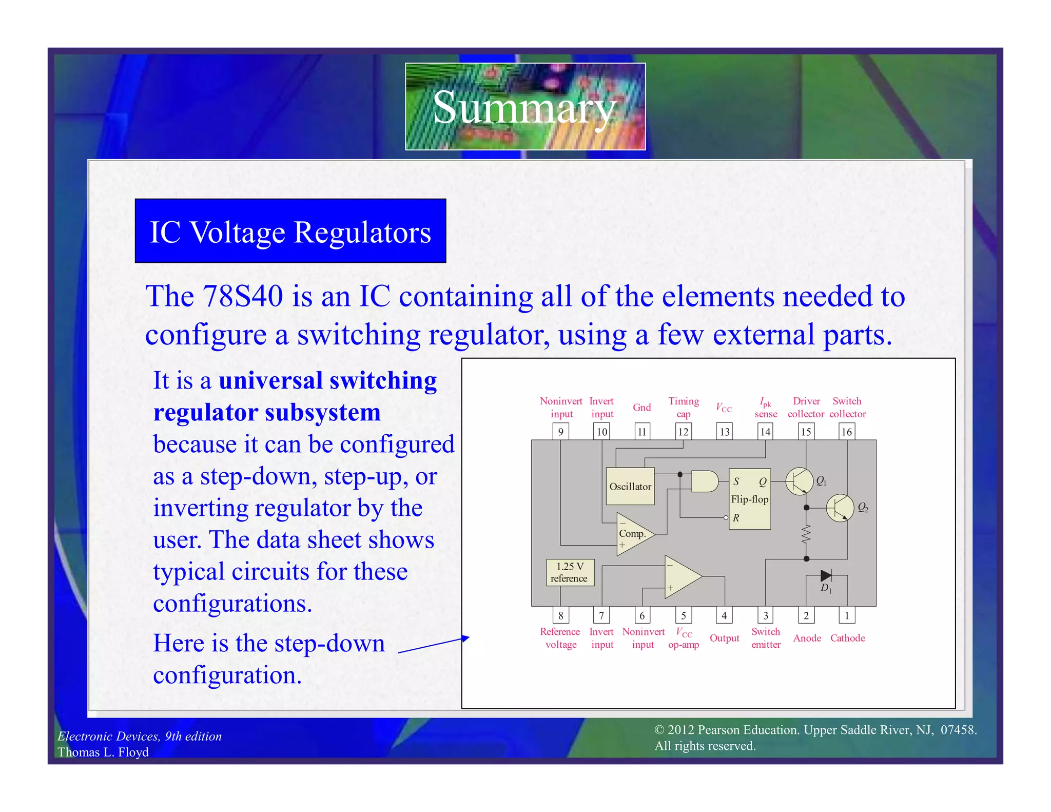
© 2012 Pearson Education. Upper Saddle River, NJ, 07458.
All rights reserved.
Electronic Devices, 9th edition
Thomas L. Floyd
Electronic Devices
Ninth Edition
Floyd
Chapter 17
© 2012 Pearson Education. Upper Saddle River, NJ, 07458.
All rights reserved.
Electronic Devices, 9th edition
Thomas L. Floyd
Power Supply Regulation
An ideal power supply provides a constant dc voltage despite
changes to the input voltage or load conditions.
Summary
0
0 Current
Voltage
Ideal power supply
The output voltage of a real power supply changes under load as shown
in the second plot. The output is also sensitive to input voltage changes.
0
0 Current
Voltage
Real power supply
VNL VNL
VFL
© 2012 Pearson Education. Upper Saddle River, NJ, 07458.
All rights reserved.
Electronic Devices, 9th edition
Thomas L. Floyd
Line Regulation
Line regulation is a measure of how well a power supply is
able to maintain the dc output voltage for a change in the ac
input line voltage. The formula for line regulation is
Summary
OUT
IN
Line Regulation = 100%
V
V
 

 

 
Line regulation can also be expressed in terms of percent
change in VOUT per volt change on the VIN (%/V).
 
OUT OUT
IN
/ 100%
Line Regulation =
V V
V


© 2012 Pearson Education. Upper Saddle River, NJ, 07458.
All rights reserved.
Electronic Devices, 9th edition
Thomas L. Floyd
Load Regulation
Load regulation is a measure of how well a power supply is
able to maintain the dc output voltage between no load and
full load with the input voltage constant. It can be expressed as
a percentage change in load voltage:
Summary
NL FL
FL
Load Regulation = 100%
V V
V
 

 
 
Load regulation can also be expressed in terms of percent
change in the output per mA change in load current (%/mA).
Sometimes a maximum error voltage is given in the specification as
illustrated in the next slide for a commercial power supply.
© 2012 Pearson Education. Upper Saddle River, NJ, 07458.
All rights reserved.
Electronic Devices, 9th edition
Thomas L. Floyd
Load Regulation
Summary
Commercial power supplies, such as you have in lab, have
excellent line and load regulation specifications.
The BK Precision 1651A is an example of
a triple output supply (two 0-24 V outputs
and a fixed 5 V output). Voltage regulation
specifications for this power supply are:
Line regulation: ≤0.01% +3 mV (Main supply)
≤5 mV (Fixed 5 V supply)
Load regulation: ≤0.01%+3 mV (Main supply)
≤5 mV (Fixed 5 V supply)
© 2012 Pearson Education. Upper Saddle River, NJ, 07458.
All rights reserved.
Electronic Devices, 9th edition
Thomas L. Floyd
Load Regulation
Sometimes the equivalent Thevenin resistance of a supply is
specified in place of a load regulation specification.
Summary
RTH = ROUT
RL
VTH = VNL
VOUT
Power Supply
In this case, VOUT can be found by
applying the voltage divider rule:
L
OUT NL
OUT L
R
V V
R R
 
  

 
In terms of resistances, load
regulation can be expressed as:
OUT
FL
Load regulation 100%
R
R
 
  
 
© 2012 Pearson Education. Upper Saddle River, NJ, 07458.
All rights reserved.
Electronic Devices, 9th edition
Thomas L. Floyd
Load Regulation
Summary
A power supply has an output resistance of 25 mW and a full
load current of 0.50 A to a 10.0 W load.
(a) What is the load regulation?
(b) What is the no load output voltage?
OUT
FL
0.025
Load regulation 100% 100%
10.0
R
R
  W
 
 
   
W
 
 
= 0.25%
(a)
(b) By Ohm’s law, VOUT = 5.0 V.
OUT
NL
L
OUT L
5.0 V
10.0
0.025 + 10.0
V
V
R
R R
 
W
   
 
  W W
 

 
= 5.013 V
© 2012 Pearson Education. Upper Saddle River, NJ, 07458.
All rights reserved.
Electronic Devices, 9th edition
Thomas L. Floyd
Series Regulators
Series Regulator block diagram:
Summary
Basic series regulator circuit:
VIN VOUT
Error
detector
Sample
circuit
Control
element
Reference
voltage
VIN VOUT
R1
Control element
Q1
D1
VREF
+
– Error detector
R2
R3
Sample
circuit
The control element maintains
a constant output voltage by
varying the collector-emitter
voltage across the transistor.
© 2012 Pearson Education. Upper Saddle River, NJ, 07458.
All rights reserved.
Electronic Devices, 9th edition
Thomas L. Floyd
Series Regulators
Summary
The output voltage for the series regulator circuit is: 2
OUT REF
3
1
R
V V
R
 
 
 
 
(a) What is the output voltage for the series regulator?
(b) If the load current is 200 mA, what is the power
dissipated by Q1?
2
OUT REF
3
1
100 k
1+ 3.9 V
47 k
R
V V
R
 
 
 
 
W
 
  
W
 
(a)
(b)
VIN VOUT
R1
Q1
D1
VREF
+
– R2
R3
47 kW
100 kW
3.9 V
18 V
4.7 kW
= 12.2 V
P = VI
= (18 V – 12.2 V)(0.2 A)
= 1.16 W
© 2012 Pearson Education. Upper Saddle River, NJ, 07458.
All rights reserved.
Electronic Devices, 9th edition
Thomas L. Floyd
Series Regulators
Summary
Current limiting prevents excessive load current. Q2 will
conduct when the current through R4 develops 0.7 V across
Q2’s VBE. This reduces base current to Q1, limiting the load
current.
VIN VOUT
R1
Q1
R3
R2
Q2
Current limiter
R4
+
–
The current limit is:
L(max)
4
0.7 V
I
R

For example, a 1.4 W
resistor, limits current
to about 0.5 A.
© 2012 Pearson Education. Upper Saddle River, NJ, 07458.
All rights reserved.
Electronic Devices, 9th edition
Thomas L. Floyd
Series Regulators
Summary
5
R5 OUT
5 6
R
V V
R R
 
  

 
An overload causes VR5 to
drop because VOUT drops.
This means that less
current is needed to
maintain conduction in Q2
and the load current drops.
+VIN VOUT
R1
Q1
+
–
Q2
R4
D1
R3
R2
R6
R5
Fold-back current limiting drops the load current well
below the peak during overload conditions. Q2 conducts
when VR5 +VBE = VR4 and begins current limiting. VR5 is
found by applying the voltage-divider rule:
© 2012 Pearson Education. Upper Saddle River, NJ, 07458.
All rights reserved.
Electronic Devices, 9th edition
Thomas L. Floyd
Shunt Regulators
Shunt Regulator block diagram:
Summary
Basic shunt regulator circuit:
VIN
R1
VOUT
Control
element
(shunt)
Sample
circuit
Error
detector
Reference
voltage
VIN
VOUT
R2
Q1
–
+
D1
R4
R3
RL
VREF
Error detector
Control
element
Sample
circuit
R1
The control element maintains
a constant output voltage by
varying the collector current in
the transistor.
© 2012 Pearson Education. Upper Saddle River, NJ, 07458.
All rights reserved.
Electronic Devices, 9th edition
Thomas L. Floyd
Shunt Regulators
Summary
Although it is less efficient
than the series regulator, the
shunt regulator has inherent
short-circuit protection. The
maximum current when the
output is shorted is VIN/R1.
Shunt regulators use a parallel transistor for the control
element. If the output voltage changes, the op-amp senses
the change and corrects the bias on Q1 to follow. For
example, a decrease in output voltage causes a decrease in
VB and an increase in VC. VIN
VOUT
R2
Q1
–
+
D1
R4
R3
RL
VREF
Error detector
Control
element
Sample
circuit
R1
© 2012 Pearson Education. Upper Saddle River, NJ, 07458.
All rights reserved.
Electronic Devices, 9th edition
Thomas L. Floyd
Switching Regulators
Summary
All switching regulators control the output voltage by
rapidly switching the input voltage on and off with a duty
cycle that depends on the load. Because they use high
frequency switching, they tend to be electrically noisy.
VC
ton toff ton toff ton toff ton
VC
VC
ton toff ton toff ton toff ton
on/off
control
VOUT
An increase in the duty cycle increases the output voltage.
A decrease in the duty cycle decreases the output voltage.
© 2012 Pearson Education. Upper Saddle River, NJ, 07458.
All rights reserved.
Electronic Devices, 9th edition
Thomas L. Floyd
Switching Regulators
Summary
A step-down switching regulator controls the output
voltage by controlling the duty cycle to a series transistor.
The duty cycle changes depending on the load requirement.
VIN
VOUT
R1
Q1
R3
R2
RL
D1
–
+
D2
Variable
pulse-width
oscillator
VREF
L
C
Because the transistor is
either ON or OFF on all
switching regulators, the
power dissipated in the
transistor is very small
and the regulator is very
efficient. The pulses are
smoothed by an LC filter.
on
C charges
+ 
VIN
VOUT
R1
Q1
R3
R2
RL
D1
–
+
D2
Variable
pulse-width
oscillator
VREF
L
C
 +
L reverses polarity
off
© 2012 Pearson Education. Upper Saddle River, NJ, 07458.
All rights reserved.
Electronic Devices, 9th edition
Thomas L. Floyd
VIN
VOUT
R1
Q1
R3
R2
RL
D1
C
D2
V
ariable
pulse-width
oscillator
L
+
+
+
–
C discharges
+ 
on
off
L field builds
Switching Regulators
Summary
In a step-up switching regulator, the control element
operates as a rapidly pulsing switch to ground. The switch
on and off times are controlled by the output voltage.
Step-up action is due to
the fact the inductor
changes polarity during
switching and adds to
VIN. Thus, the output
voltage is larger than
the input voltage.
VIN
VOUT
R1
Q1
R3
R2
RL
D1
C
D2
V
ariable
pulse-width
oscillator
L
+
+
+
–
on
off
C charges
 +
L field collapses
VIN
VOUT
R1
Q1
R3
R2
RL
D1
C
D2
V
ariable
pulse-width
oscillator
L
+
+
+
–
© 2012 Pearson Education. Upper Saddle River, NJ, 07458.
All rights reserved.
Electronic Devices, 9th edition
Thomas L. Floyd
+VIN
–VOUT
R1
Q1
R3
R2 RL
D1
D2
Variable
pulse-width
oscillator
L
+
–
C
+

on
off
L field builds
C discharges
Switching Regulators
In a voltage-inverter switching regulator, the output is the
opposite polarity of the input. It can be used in conjunction
with a positive regulator from the same input source.
Inversion occurs
because the inductor
reverses polarity
when the diode
conducts, charging
the capacitor with
the opposite polarity
of the input.
Summary
+VIN
–VOUT
R1
Q1
R3
R2 RL
D1
D2
Variable
pulse-width
oscillator
L
+
–
C
on
L field collapses

+ C charges
off
+VIN
–VOUT
R1
Q1
R3
R2 RL
D1
D2
Variable
pulse-width
oscillator
L
+
–
C
© 2012 Pearson Education. Upper Saddle River, NJ, 07458.
All rights reserved.
Electronic Devices, 9th edition
Thomas L. Floyd
IC Voltage Regulators
Integrated circuit voltage regulators are available as
series regulators or as switching regulators. The popular
three-terminal regulators are often used on separate pc
boards within a system because they are inexpensive and
avoid problems associated with large power distribution
systems (such as noise pickup).
Summary
1
2
3
1 2
3
4
Type number Output voltage
7805
7806
7808
7809
7812
7815
7818
7824
+5.0 V
+6.0 V
+8.0 V
+9.0 V
+12.0 V
+15.0 V
+18.0 V
+24.0 V
78XX Regulators
The 78XX series is a fixed
positive output regulator
available in various
packages and with
standard voltage outputs.
TO-220 case
D-PAK
© 2012 Pearson Education. Upper Saddle River, NJ, 07458.
All rights reserved.
Electronic Devices, 9th edition
Thomas L. Floyd
IC Voltage Regulators
The only external components required
with the 78XX series are input and output
capacitors and some form of heat sink.
These IC’s include thermal shutdown
protection and internal current limiting.
Summary
Positive
input
Gnd
Positive
output
78XX
(1)
(2)
(3)
The 78XX series are
primarily used for fixed
output voltages, but with
additional components, they
can be set up for variable
voltages or currents.
1
2
3
1 2
3
4
Heat-sink surface
© 2012 Pearson Education. Upper Saddle River, NJ, 07458.
All rights reserved.
Electronic Devices, 9th edition
Thomas L. Floyd
IC Voltage Regulators
The 79XX series is the negative output counterpart to the
78XX series, however the pin assignments are different
on this series. Other specifications are basically the same.
Summary
Negative
input
Gnd
Negative
output
79XX
(1)
(2) (3) 7905
7905.2
7906
7908
7912
7915
7918
7924
–5.0 V
–5.2 V
–6.0 V
–8.0 V
–12.0 V
–15.0 V
–18.0 V
–24.0 V
Type number Output voltage
© 2012 Pearson Education. Upper Saddle River, NJ, 07458.
All rights reserved.
Electronic Devices, 9th edition
Thomas L. Floyd
IC Voltage Regulators
The LM317 is a adjustable positive output IC regulator.
There is a fixed reference voltage of +1.25 V between the
output and adjustment terminals. There is no ground pin.
Summary
The output voltage is calculated by: 2
OUT REF ADJ 2
1
1
R
V V I R
R
 
  
 
 
Adjustment
R1
R2
C1
C2
C3
Positive
input
Positive
output
(1)
(3) (2)
LM317
What is VOUT?
(Assume IADJ = 50 mA.)
= 16.8 V
R1
R2
C1
C2
C3
(1)
(3) (2)
LM317
  
OUT
2 kΩ
1.25 V 1 50 μA 2 k
150
V
 
   W
 
W
 
2 kW
150 W
+20 V +16.8 V
© 2012 Pearson Education. Upper Saddle River, NJ, 07458.
All rights reserved.
Electronic Devices, 9th edition
Thomas L. Floyd
IC Voltage Regulators
IC regulators are limited to a maximum allowable current
before shutting down. The circuit shown is uses an
external pass transistor to increase the maximum available
load current.
Summary
VIN
RL
Rext
Qext
VOUT
C1
C2
78XX
Rext sets the point where
Qext begins to conduct:
ext
max
0.7 V
R
I

For example, if Imax is
1.0 A, Rext = 0.7 W
What minimum power rating is required for Rext?
P = I2R = (1 A)2(0.7 W) = 0.7 W
© 2012 Pearson Education. Upper Saddle River, NJ, 07458.
All rights reserved.
Electronic Devices, 9th edition
Thomas L. Floyd
IC Voltage Regulators
The 78S40 is an IC containing all of the elements needed to
configure a switching regulator, using a few external parts.
Summary
It is a universal switching
regulator subsystem
because it can be configured
as a step-down, step-up, or
inverting regulator by the
user. The data sheet shows
typical circuits for these
configurations.
–
+
10 11 12 13 14 15 16
7 6 5 4 3 2 1
–
+
Q1
Q2
S
Oscillator
R
Q
Comp.
Flip-flop
VOUT
R1
L
CO
R2
VIN
CT
RCS
VCC
1.25 V
reference
D1
8
9
–
+
9 10 11 12 13 14 15 16
Noninvert
input
Invert
input
Gnd
Timing
cap
VCC
Ipk
sense
Driver
collector
Switch
collector
8 7 6 5 4 3 2 1
Reference
voltage
Invert
input
Noninvert
input
VCC
op-amp
Output
Switch
emitter
Anode Cathode
–
+
Q1
Q2
S
Oscillator
R
Q
Comp.
Flip-flop
1.25 V
reference
D1
Here is the step-down
configuration.
© 2012 Pearson Education. Upper Saddle River, NJ, 07458.
All rights reserved.
Electronic Devices, 9th edition
Thomas L. Floyd
Selected Key Terms
Regulator
Line regulation
Load regulation
Linear regulator
Switching
regulator
A electronic circuit that maintains an
essentially constant output voltage with
changing input voltage or load current.
The percentage change in output voltage for a
given change in input (line) voltage.
The percentage change in output voltage for a
given change in load current.
A voltage regulator in which the control
element operates in the linear region.
A voltage regulator in which the control
element operates as a switch.

Chapter 17 Regulators.pdf

  • 1.
    © 2012 PearsonEducation. Upper Saddle River, NJ, 07458. All rights reserved. Electronic Devices, 9th edition Thomas L. Floyd Electronic Devices Ninth Edition Floyd Chapter 17
  • 2.
    © 2012 PearsonEducation. Upper Saddle River, NJ, 07458. All rights reserved. Electronic Devices, 9th edition Thomas L. Floyd Power Supply Regulation An ideal power supply provides a constant dc voltage despite changes to the input voltage or load conditions. Summary 0 0 Current Voltage Ideal power supply The output voltage of a real power supply changes under load as shown in the second plot. The output is also sensitive to input voltage changes. 0 0 Current Voltage Real power supply VNL VNL VFL
  • 3.
    © 2012 PearsonEducation. Upper Saddle River, NJ, 07458. All rights reserved. Electronic Devices, 9th edition Thomas L. Floyd Line Regulation Line regulation is a measure of how well a power supply is able to maintain the dc output voltage for a change in the ac input line voltage. The formula for line regulation is Summary OUT IN Line Regulation = 100% V V         Line regulation can also be expressed in terms of percent change in VOUT per volt change on the VIN (%/V).   OUT OUT IN / 100% Line Regulation = V V V  
  • 4.
    © 2012 PearsonEducation. Upper Saddle River, NJ, 07458. All rights reserved. Electronic Devices, 9th edition Thomas L. Floyd Load Regulation Load regulation is a measure of how well a power supply is able to maintain the dc output voltage between no load and full load with the input voltage constant. It can be expressed as a percentage change in load voltage: Summary NL FL FL Load Regulation = 100% V V V        Load regulation can also be expressed in terms of percent change in the output per mA change in load current (%/mA). Sometimes a maximum error voltage is given in the specification as illustrated in the next slide for a commercial power supply.
  • 5.
    © 2012 PearsonEducation. Upper Saddle River, NJ, 07458. All rights reserved. Electronic Devices, 9th edition Thomas L. Floyd Load Regulation Summary Commercial power supplies, such as you have in lab, have excellent line and load regulation specifications. The BK Precision 1651A is an example of a triple output supply (two 0-24 V outputs and a fixed 5 V output). Voltage regulation specifications for this power supply are: Line regulation: ≤0.01% +3 mV (Main supply) ≤5 mV (Fixed 5 V supply) Load regulation: ≤0.01%+3 mV (Main supply) ≤5 mV (Fixed 5 V supply)
  • 6.
    © 2012 PearsonEducation. Upper Saddle River, NJ, 07458. All rights reserved. Electronic Devices, 9th edition Thomas L. Floyd Load Regulation Sometimes the equivalent Thevenin resistance of a supply is specified in place of a load regulation specification. Summary RTH = ROUT RL VTH = VNL VOUT Power Supply In this case, VOUT can be found by applying the voltage divider rule: L OUT NL OUT L R V V R R         In terms of resistances, load regulation can be expressed as: OUT FL Load regulation 100% R R       
  • 7.
    © 2012 PearsonEducation. Upper Saddle River, NJ, 07458. All rights reserved. Electronic Devices, 9th edition Thomas L. Floyd Load Regulation Summary A power supply has an output resistance of 25 mW and a full load current of 0.50 A to a 10.0 W load. (a) What is the load regulation? (b) What is the no load output voltage? OUT FL 0.025 Load regulation 100% 100% 10.0 R R   W         W     = 0.25% (a) (b) By Ohm’s law, VOUT = 5.0 V. OUT NL L OUT L 5.0 V 10.0 0.025 + 10.0 V V R R R   W         W W      = 5.013 V
  • 8.
    © 2012 PearsonEducation. Upper Saddle River, NJ, 07458. All rights reserved. Electronic Devices, 9th edition Thomas L. Floyd Series Regulators Series Regulator block diagram: Summary Basic series regulator circuit: VIN VOUT Error detector Sample circuit Control element Reference voltage VIN VOUT R1 Control element Q1 D1 VREF + – Error detector R2 R3 Sample circuit The control element maintains a constant output voltage by varying the collector-emitter voltage across the transistor.
  • 9.
    © 2012 PearsonEducation. Upper Saddle River, NJ, 07458. All rights reserved. Electronic Devices, 9th edition Thomas L. Floyd Series Regulators Summary The output voltage for the series regulator circuit is: 2 OUT REF 3 1 R V V R         (a) What is the output voltage for the series regulator? (b) If the load current is 200 mA, what is the power dissipated by Q1? 2 OUT REF 3 1 100 k 1+ 3.9 V 47 k R V V R         W      W   (a) (b) VIN VOUT R1 Q1 D1 VREF + – R2 R3 47 kW 100 kW 3.9 V 18 V 4.7 kW = 12.2 V P = VI = (18 V – 12.2 V)(0.2 A) = 1.16 W
  • 10.
    © 2012 PearsonEducation. Upper Saddle River, NJ, 07458. All rights reserved. Electronic Devices, 9th edition Thomas L. Floyd Series Regulators Summary Current limiting prevents excessive load current. Q2 will conduct when the current through R4 develops 0.7 V across Q2’s VBE. This reduces base current to Q1, limiting the load current. VIN VOUT R1 Q1 R3 R2 Q2 Current limiter R4 + – The current limit is: L(max) 4 0.7 V I R  For example, a 1.4 W resistor, limits current to about 0.5 A.
  • 11.
    © 2012 PearsonEducation. Upper Saddle River, NJ, 07458. All rights reserved. Electronic Devices, 9th edition Thomas L. Floyd Series Regulators Summary 5 R5 OUT 5 6 R V V R R         An overload causes VR5 to drop because VOUT drops. This means that less current is needed to maintain conduction in Q2 and the load current drops. +VIN VOUT R1 Q1 + – Q2 R4 D1 R3 R2 R6 R5 Fold-back current limiting drops the load current well below the peak during overload conditions. Q2 conducts when VR5 +VBE = VR4 and begins current limiting. VR5 is found by applying the voltage-divider rule:
  • 12.
    © 2012 PearsonEducation. Upper Saddle River, NJ, 07458. All rights reserved. Electronic Devices, 9th edition Thomas L. Floyd Shunt Regulators Shunt Regulator block diagram: Summary Basic shunt regulator circuit: VIN R1 VOUT Control element (shunt) Sample circuit Error detector Reference voltage VIN VOUT R2 Q1 – + D1 R4 R3 RL VREF Error detector Control element Sample circuit R1 The control element maintains a constant output voltage by varying the collector current in the transistor.
  • 13.
    © 2012 PearsonEducation. Upper Saddle River, NJ, 07458. All rights reserved. Electronic Devices, 9th edition Thomas L. Floyd Shunt Regulators Summary Although it is less efficient than the series regulator, the shunt regulator has inherent short-circuit protection. The maximum current when the output is shorted is VIN/R1. Shunt regulators use a parallel transistor for the control element. If the output voltage changes, the op-amp senses the change and corrects the bias on Q1 to follow. For example, a decrease in output voltage causes a decrease in VB and an increase in VC. VIN VOUT R2 Q1 – + D1 R4 R3 RL VREF Error detector Control element Sample circuit R1
  • 14.
    © 2012 PearsonEducation. Upper Saddle River, NJ, 07458. All rights reserved. Electronic Devices, 9th edition Thomas L. Floyd Switching Regulators Summary All switching regulators control the output voltage by rapidly switching the input voltage on and off with a duty cycle that depends on the load. Because they use high frequency switching, they tend to be electrically noisy. VC ton toff ton toff ton toff ton ton toff ton toff ton toff ton VC VC ton toff ton toff ton toff ton on/off control VOUT An increase in the duty cycle increases the output voltage. A decrease in the duty cycle decreases the output voltage.
  • 15.
    © 2012 PearsonEducation. Upper Saddle River, NJ, 07458. All rights reserved. Electronic Devices, 9th edition Thomas L. Floyd Switching Regulators Summary A step-down switching regulator controls the output voltage by controlling the duty cycle to a series transistor. The duty cycle changes depending on the load requirement. VIN VOUT R1 Q1 R3 R2 RL D1 – + D2 Variable pulse-width oscillator VREF L C Because the transistor is either ON or OFF on all switching regulators, the power dissipated in the transistor is very small and the regulator is very efficient. The pulses are smoothed by an LC filter. on C charges +  VIN VOUT R1 Q1 R3 R2 RL D1 – + D2 Variable pulse-width oscillator VREF L C  + L reverses polarity off
  • 16.
    © 2012 PearsonEducation. Upper Saddle River, NJ, 07458. All rights reserved. Electronic Devices, 9th edition Thomas L. Floyd VIN VOUT R1 Q1 R3 R2 RL D1 C D2 V ariable pulse-width oscillator L + + + – C discharges +  on off L field builds Switching Regulators Summary In a step-up switching regulator, the control element operates as a rapidly pulsing switch to ground. The switch on and off times are controlled by the output voltage. Step-up action is due to the fact the inductor changes polarity during switching and adds to VIN. Thus, the output voltage is larger than the input voltage. VIN VOUT R1 Q1 R3 R2 RL D1 C D2 V ariable pulse-width oscillator L + + + – on off C charges  + L field collapses VIN VOUT R1 Q1 R3 R2 RL D1 C D2 V ariable pulse-width oscillator L + + + –
  • 17.
    © 2012 PearsonEducation. Upper Saddle River, NJ, 07458. All rights reserved. Electronic Devices, 9th edition Thomas L. Floyd +VIN –VOUT R1 Q1 R3 R2 RL D1 D2 Variable pulse-width oscillator L + – C +  on off L field builds C discharges Switching Regulators In a voltage-inverter switching regulator, the output is the opposite polarity of the input. It can be used in conjunction with a positive regulator from the same input source. Inversion occurs because the inductor reverses polarity when the diode conducts, charging the capacitor with the opposite polarity of the input. Summary +VIN –VOUT R1 Q1 R3 R2 RL D1 D2 Variable pulse-width oscillator L + – C on L field collapses  + C charges off +VIN –VOUT R1 Q1 R3 R2 RL D1 D2 Variable pulse-width oscillator L + – C
  • 18.
    © 2012 PearsonEducation. Upper Saddle River, NJ, 07458. All rights reserved. Electronic Devices, 9th edition Thomas L. Floyd IC Voltage Regulators Integrated circuit voltage regulators are available as series regulators or as switching regulators. The popular three-terminal regulators are often used on separate pc boards within a system because they are inexpensive and avoid problems associated with large power distribution systems (such as noise pickup). Summary 1 2 3 1 2 3 4 Type number Output voltage 7805 7806 7808 7809 7812 7815 7818 7824 +5.0 V +6.0 V +8.0 V +9.0 V +12.0 V +15.0 V +18.0 V +24.0 V 78XX Regulators The 78XX series is a fixed positive output regulator available in various packages and with standard voltage outputs. TO-220 case D-PAK
  • 19.
    © 2012 PearsonEducation. Upper Saddle River, NJ, 07458. All rights reserved. Electronic Devices, 9th edition Thomas L. Floyd IC Voltage Regulators The only external components required with the 78XX series are input and output capacitors and some form of heat sink. These IC’s include thermal shutdown protection and internal current limiting. Summary Positive input Gnd Positive output 78XX (1) (2) (3) The 78XX series are primarily used for fixed output voltages, but with additional components, they can be set up for variable voltages or currents. 1 2 3 1 2 3 4 Heat-sink surface
  • 20.
    © 2012 PearsonEducation. Upper Saddle River, NJ, 07458. All rights reserved. Electronic Devices, 9th edition Thomas L. Floyd IC Voltage Regulators The 79XX series is the negative output counterpart to the 78XX series, however the pin assignments are different on this series. Other specifications are basically the same. Summary Negative input Gnd Negative output 79XX (1) (2) (3) 7905 7905.2 7906 7908 7912 7915 7918 7924 –5.0 V –5.2 V –6.0 V –8.0 V –12.0 V –15.0 V –18.0 V –24.0 V Type number Output voltage
  • 21.
    © 2012 PearsonEducation. Upper Saddle River, NJ, 07458. All rights reserved. Electronic Devices, 9th edition Thomas L. Floyd IC Voltage Regulators The LM317 is a adjustable positive output IC regulator. There is a fixed reference voltage of +1.25 V between the output and adjustment terminals. There is no ground pin. Summary The output voltage is calculated by: 2 OUT REF ADJ 2 1 1 R V V I R R          Adjustment R1 R2 C1 C2 C3 Positive input Positive output (1) (3) (2) LM317 What is VOUT? (Assume IADJ = 50 mA.) = 16.8 V R1 R2 C1 C2 C3 (1) (3) (2) LM317    OUT 2 kΩ 1.25 V 1 50 μA 2 k 150 V      W   W   2 kW 150 W +20 V +16.8 V
  • 22.
    © 2012 PearsonEducation. Upper Saddle River, NJ, 07458. All rights reserved. Electronic Devices, 9th edition Thomas L. Floyd IC Voltage Regulators IC regulators are limited to a maximum allowable current before shutting down. The circuit shown is uses an external pass transistor to increase the maximum available load current. Summary VIN RL Rext Qext VOUT C1 C2 78XX Rext sets the point where Qext begins to conduct: ext max 0.7 V R I  For example, if Imax is 1.0 A, Rext = 0.7 W What minimum power rating is required for Rext? P = I2R = (1 A)2(0.7 W) = 0.7 W
  • 23.
    © 2012 PearsonEducation. Upper Saddle River, NJ, 07458. All rights reserved. Electronic Devices, 9th edition Thomas L. Floyd IC Voltage Regulators The 78S40 is an IC containing all of the elements needed to configure a switching regulator, using a few external parts. Summary It is a universal switching regulator subsystem because it can be configured as a step-down, step-up, or inverting regulator by the user. The data sheet shows typical circuits for these configurations. – + 10 11 12 13 14 15 16 7 6 5 4 3 2 1 – + Q1 Q2 S Oscillator R Q Comp. Flip-flop VOUT R1 L CO R2 VIN CT RCS VCC 1.25 V reference D1 8 9 – + 9 10 11 12 13 14 15 16 Noninvert input Invert input Gnd Timing cap VCC Ipk sense Driver collector Switch collector 8 7 6 5 4 3 2 1 Reference voltage Invert input Noninvert input VCC op-amp Output Switch emitter Anode Cathode – + Q1 Q2 S Oscillator R Q Comp. Flip-flop 1.25 V reference D1 Here is the step-down configuration.
  • 24.
    © 2012 PearsonEducation. Upper Saddle River, NJ, 07458. All rights reserved. Electronic Devices, 9th edition Thomas L. Floyd Selected Key Terms Regulator Line regulation Load regulation Linear regulator Switching regulator A electronic circuit that maintains an essentially constant output voltage with changing input voltage or load current. The percentage change in output voltage for a given change in input (line) voltage. The percentage change in output voltage for a given change in load current. A voltage regulator in which the control element operates in the linear region. A voltage regulator in which the control element operates as a switch.