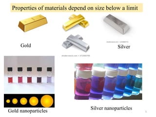
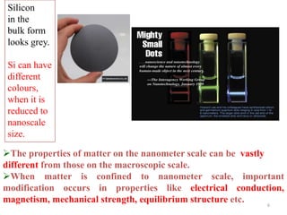
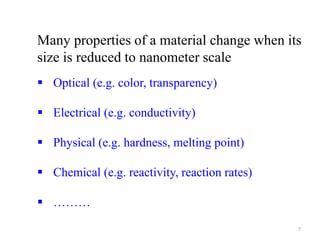
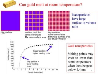
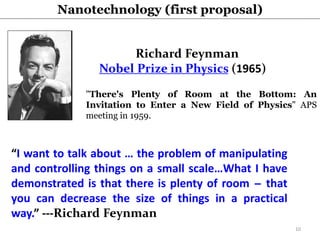
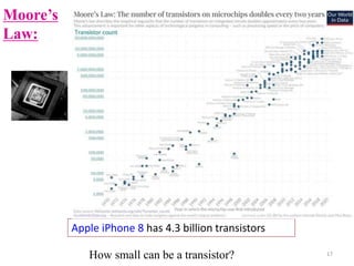
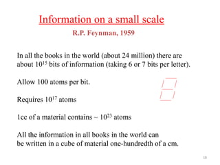
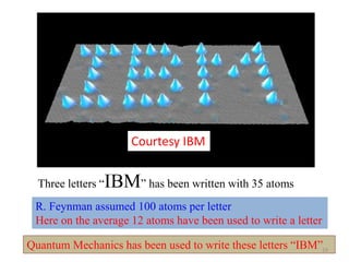
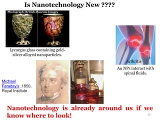
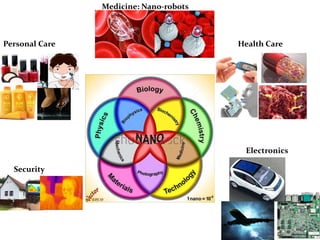
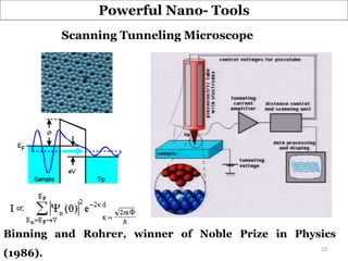
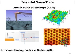
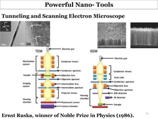
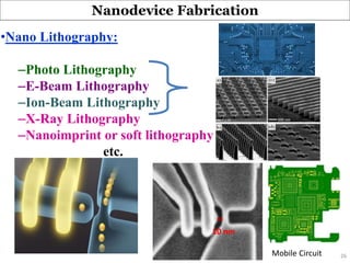
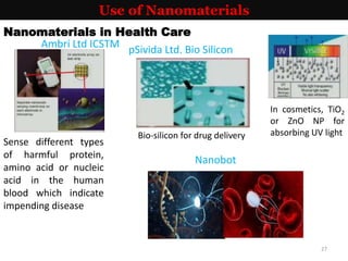
Course Name:
Introduction to Nanoscience & Nanotechnology
(Code:NT70002)
Rabaya Basori
rabaya@iitkgp.ac.in
rabeya.phy@gmail.com
1
What is nano?
It is 10-9
When the size of a material is of the order of nanometer,
(typically one of the dimensions below 100 nanometer)
it is nanoscale material or nanomaterial
The size matters
2
A meter is about the distance from
the tip of your nose to the end of
your hand (1 meter = 3.28 feet).
Millimeter- One thousandth of
meter.(10-3m)
Micron: a micron is a millionth of
a meter (or) one thousandth of
millimeter (10-6m)
Nanometer:
A nanometer is one thousandth of
a micron (10–9m)
(or) a billionth of a meter. i.e. one
billion nanometers in a meter.
a0 =0.05 nm
How much is Nanometer?
DNA
Atom (0.1 ─ 0.5 nm)
3
Gold Silver
Properties of materials depend on size below a limit
4
Gold Silver
Gold nanoparticles
Silver nanoparticles
Properties of materials depend on size below a limit
5
The properties of matter on the nanometer scale can be vastly
different from those on the macroscopic scale.
When matter is confined to nanometer scale, important
modification occurs in properties like electrical conduction,
magnetism, mechanical strength, equilibrium structure etc.
Silicon
in the
bulk form
looks grey.
Si can have
different
colours,
when it is
reduced to
nanoscale
size.
6
Many properties of a material change when its
size is reduced to nanometer scale
 Optical (e.g. color, transparency)
 Electrical (e.g. conductivity)
 Physical (e.g. hardness, melting point)
 Chemical (e.g. reactivity, reaction rates)
 ………
7
Can gold melt at room temperature?
Nanoparticles
have large
surface-to-volume
ratio
Gold nanoparticles
Melting points may
even be lower than
room temperature
when the size goes
below 1.4 nm 8
What is Nanoscience & Technology
Find the science of nanomaterials Utilization in Technological application
Nanotechnology
9
"There's Plenty of Room at the Bottom: An
Invitation to Enter a New Field of Physics" APS
meeting in 1959.
Richard Feynman
Nobel Prize in Physics (1965)
“I want to talk about … the problem of manipulating
and controlling things on a small scale…What I have
demonstrated is that there is plenty of room ̶ that
you can decrease the size of things in a practical
way.” ---Richard Feynman
Nanotechnology (first proposal)
10
Feynman Prize
Feynman offered $1,000 to anyone who could:
1. Build a motor that would fit inside a 1/64”x 1/64”x 1/64”
box.
2. Write a page of text with letters that are small enough for the
Encyclopedia Britannica could be printed on the head of a
pin.
First Feynman Prize
William McLellan claimed the 1st prize within a year by
making motor by hand. Feynman hadn’t made this challenge
hard enough. This prize was won without creating any new
technology.
11
Second Feynman Prize
1985: Tom Newman and Fabian Pease (Stanford University) used
e-beam lithography to write a part of A Tale of Two Cities by
Charles Dickens at the length scale represented by Feynman.
12
1st Transistor in 1947
1st Transistor
13
A Pentium® chip with 3.3 million transistors.
Such micro-processors are at the personal computers of 1990s
(Courtesy of Intel Corporation.)
14
Jack Kilby, a winner of Noble Prize in Physics (2000) for invention of
integrated circuit
Integrated Circuit
15
Made by John Bardeen and Walter
Brattain at Bell Laboratories.
Shockley, Bardeen and Brattain,
winners of Noble Prize in Physics
(1956)
Researchers from MIT and the
University of Colorado made 3-D
transistors as narrow as 2.5
nanometers
1st Transistor in 1947 Transistor in 2018
Transistor Size Reduction
16
Moore’s
Law:
Pentium 4
Apple iPhone 8 has 4.3 billion transistors
How small can be a transistor? 17
Information on a small scale
In all the books in the world (about 24 million) there are
about 1015 bits of information (taking 6 or 7 bits per letter).
Allow 100 atoms per bit.
Requires 1017 atoms
1cc of a material contains ~ 1023 atoms
All the information in all books in the world can
be written in a cube of material one-hundredth of a cm.
R.P. Feynman, 1959
18
Courtesy IBM
Three letters “IBM” has been written with 35 atoms
R. Feynman assumed 100 atoms per letter
Here on the average 12 atoms have been used to write a letter
Quantum Mechanics has been used to write these letters “IBM”19
Photograph: British Museum Images
Lycurgus glass containing gold-
silver alloyed nanoparticles.
Au NPs interact with
spinal fluids.
Arthritis
Is Nanotechnology New ????
Nanotechnology is already around us if we
know where to look! 20
Michael
Faraday’s ,1850,
Royal Institute
It is the combination of existing technology
and our newly found ability to observe and
manipulate down to atomic level that makes
nanotechnology so compelling from scientific
and business point of view.
Nanotechnology is not new.
21
Personal Care Health Care
Security
Electronics
Medicine: Nano-robots
22
Powerful Nano- Tools
Binning and Rohrer, winner of Noble Prize in Physics
(1986).
Scanning Tunneling Microscope
23
Powerful Nano- Tools
Inventors: Binning, Quate and Gerber, 1986.
Atomic Force Microscope (AFM)
24
Powerful Nano- Tools
Tunneling and Scanning Electron Microscope
Ernst Ruska, winner of Noble Prize in Physics (1986).
25
•Nano Lithography:
–Photo Lithography
–E-Beam Lithography
–Ion-Beam Lithography
–X-Ray Lithography
–Nanoimprint or soft lithography
etc.
Nanodevice Fabrication
Mobile Circuit
10 nm
26
Use of Nanomaterials
Nanomaterials in Health Care
pSivida Ltd. Bio Silicon
Bio-silicon for drug delivery
Ambri Ltd ICSTM
Sense different types
of harmful protein,
amino acid or nucleic
acid in the human
blood which indicate
impending disease
In cosmetics, TiO2
or ZnO NP for
absorbing UV light
Nanobot
27
28
Use of Nanomaterials
Nanomaterials in Chips
Graphene
Good thermal conductor
One of the best electrical conductor
Transparent
29
Use of Nanomaterials in Lighting/Displays
Nanotechnology to increases the brightness,
efficiency and clarity of LEDs, which are widely
used in smartphones and other electronics.
30
Controlled release of pesticides/fungicides/nutrients from
nanocoating
Agriculture
31
The Future of Agriculture?
Vertical farming
Indoor Farms Powered by LEDs
Growth rate is 2.5 times (latest 5 times) higher.
Yield of the plant from 50% to 90%, Light Recipes.
Water usage only 1% compared with outside. 32
Vertical farming
using LED lights
33
34
Thank you

1_Nanotechnology Introduction.pptx

  • 1.
    Course Name: Introduction toNanoscience & Nanotechnology (Code:NT70002) Rabaya Basori rabaya@iitkgp.ac.in rabeya.phy@gmail.com 1
  • 2.
    What is nano? Itis 10-9 When the size of a material is of the order of nanometer, (typically one of the dimensions below 100 nanometer) it is nanoscale material or nanomaterial The size matters 2
  • 3.
    A meter isabout the distance from the tip of your nose to the end of your hand (1 meter = 3.28 feet). Millimeter- One thousandth of meter.(10-3m) Micron: a micron is a millionth of a meter (or) one thousandth of millimeter (10-6m) Nanometer: A nanometer is one thousandth of a micron (10–9m) (or) a billionth of a meter. i.e. one billion nanometers in a meter. a0 =0.05 nm How much is Nanometer? DNA Atom (0.1 ─ 0.5 nm) 3
  • 4.
    Gold Silver Properties ofmaterials depend on size below a limit 4
  • 5.
    Gold Silver Gold nanoparticles Silvernanoparticles Properties of materials depend on size below a limit 5
  • 6.
    The properties ofmatter on the nanometer scale can be vastly different from those on the macroscopic scale. When matter is confined to nanometer scale, important modification occurs in properties like electrical conduction, magnetism, mechanical strength, equilibrium structure etc. Silicon in the bulk form looks grey. Si can have different colours, when it is reduced to nanoscale size. 6
  • 7.
    Many properties ofa material change when its size is reduced to nanometer scale  Optical (e.g. color, transparency)  Electrical (e.g. conductivity)  Physical (e.g. hardness, melting point)  Chemical (e.g. reactivity, reaction rates)  ……… 7
  • 8.
    Can gold meltat room temperature? Nanoparticles have large surface-to-volume ratio Gold nanoparticles Melting points may even be lower than room temperature when the size goes below 1.4 nm 8
  • 9.
    What is Nanoscience& Technology Find the science of nanomaterials Utilization in Technological application Nanotechnology 9
  • 10.
    "There's Plenty ofRoom at the Bottom: An Invitation to Enter a New Field of Physics" APS meeting in 1959. Richard Feynman Nobel Prize in Physics (1965) “I want to talk about … the problem of manipulating and controlling things on a small scale…What I have demonstrated is that there is plenty of room ̶ that you can decrease the size of things in a practical way.” ---Richard Feynman Nanotechnology (first proposal) 10
  • 11.
    Feynman Prize Feynman offered$1,000 to anyone who could: 1. Build a motor that would fit inside a 1/64”x 1/64”x 1/64” box. 2. Write a page of text with letters that are small enough for the Encyclopedia Britannica could be printed on the head of a pin. First Feynman Prize William McLellan claimed the 1st prize within a year by making motor by hand. Feynman hadn’t made this challenge hard enough. This prize was won without creating any new technology. 11
  • 12.
    Second Feynman Prize 1985:Tom Newman and Fabian Pease (Stanford University) used e-beam lithography to write a part of A Tale of Two Cities by Charles Dickens at the length scale represented by Feynman. 12
  • 13.
    1st Transistor in1947 1st Transistor 13
  • 14.
    A Pentium® chipwith 3.3 million transistors. Such micro-processors are at the personal computers of 1990s (Courtesy of Intel Corporation.) 14
  • 15.
    Jack Kilby, awinner of Noble Prize in Physics (2000) for invention of integrated circuit Integrated Circuit 15
  • 16.
    Made by JohnBardeen and Walter Brattain at Bell Laboratories. Shockley, Bardeen and Brattain, winners of Noble Prize in Physics (1956) Researchers from MIT and the University of Colorado made 3-D transistors as narrow as 2.5 nanometers 1st Transistor in 1947 Transistor in 2018 Transistor Size Reduction 16
  • 17.
    Moore’s Law: Pentium 4 Apple iPhone8 has 4.3 billion transistors How small can be a transistor? 17
  • 18.
    Information on asmall scale In all the books in the world (about 24 million) there are about 1015 bits of information (taking 6 or 7 bits per letter). Allow 100 atoms per bit. Requires 1017 atoms 1cc of a material contains ~ 1023 atoms All the information in all books in the world can be written in a cube of material one-hundredth of a cm. R.P. Feynman, 1959 18
  • 19.
    Courtesy IBM Three letters“IBM” has been written with 35 atoms R. Feynman assumed 100 atoms per letter Here on the average 12 atoms have been used to write a letter Quantum Mechanics has been used to write these letters “IBM”19
  • 20.
    Photograph: British MuseumImages Lycurgus glass containing gold- silver alloyed nanoparticles. Au NPs interact with spinal fluids. Arthritis Is Nanotechnology New ???? Nanotechnology is already around us if we know where to look! 20 Michael Faraday’s ,1850, Royal Institute
  • 21.
    It is thecombination of existing technology and our newly found ability to observe and manipulate down to atomic level that makes nanotechnology so compelling from scientific and business point of view. Nanotechnology is not new. 21
  • 22.
    Personal Care HealthCare Security Electronics Medicine: Nano-robots 22
  • 23.
    Powerful Nano- Tools Binningand Rohrer, winner of Noble Prize in Physics (1986). Scanning Tunneling Microscope 23
  • 24.
    Powerful Nano- Tools Inventors:Binning, Quate and Gerber, 1986. Atomic Force Microscope (AFM) 24
  • 25.
    Powerful Nano- Tools Tunnelingand Scanning Electron Microscope Ernst Ruska, winner of Noble Prize in Physics (1986). 25
  • 26.
    •Nano Lithography: –Photo Lithography –E-BeamLithography –Ion-Beam Lithography –X-Ray Lithography –Nanoimprint or soft lithography etc. Nanodevice Fabrication Mobile Circuit 10 nm 26
  • 27.
    Use of Nanomaterials Nanomaterialsin Health Care pSivida Ltd. Bio Silicon Bio-silicon for drug delivery Ambri Ltd ICSTM Sense different types of harmful protein, amino acid or nucleic acid in the human blood which indicate impending disease In cosmetics, TiO2 or ZnO NP for absorbing UV light Nanobot 27
  • 28.
  • 29.
    Use of Nanomaterials Nanomaterialsin Chips Graphene Good thermal conductor One of the best electrical conductor Transparent 29
  • 30.
    Use of Nanomaterialsin Lighting/Displays Nanotechnology to increases the brightness, efficiency and clarity of LEDs, which are widely used in smartphones and other electronics. 30
  • 31.
    Controlled release ofpesticides/fungicides/nutrients from nanocoating Agriculture 31
  • 32.
    The Future ofAgriculture? Vertical farming Indoor Farms Powered by LEDs Growth rate is 2.5 times (latest 5 times) higher. Yield of the plant from 50% to 90%, Light Recipes. Water usage only 1% compared with outside. 32
  • 33.
  • 34.

Editor's Notes

  • #11 Feynman considered the possibility of direct manipulation of individual atoms as a more powerful form of synthetic chemistry than those used at the time. Feynman also suggested that it should be possible, in principle, to make nanoscale machines that "arrange the atoms the way we want", and do chemical synthesis by mechanical manipulation.
  • #12 6x10⁻⁵ cc
  • #14 Made by John Bardeen and Walter Brattain at Bell Laboratories got Noble Prize in 1960.
  • #17 Made by John Bardeen and Walter Brattain at Bell Laboratories got Noble Prize in 1960.
  • #18 iPhone 12 Mini= 131.5 x 64.2 x 7.4 mm3 , 4.3 billion transistor, I transistor dimension = 1.4 e-5 mm3 = 1.4 e-14 m3
  • #22 It is the combination of existing technology and our newly found ability to observe and manipulate down to atomic level that makes nanotechnology so compelling scientific and business point of view.
  • #23 The Nobel Prize for Physics in 2010 went to Andre Geim and Kostya Novoselov “for groundbreaking experiments regarding the two-dimensional material graphene