
Recommended
More Related Content
What's hot
What's hot (20)
Similar to Microelectronic circuits and devices: chapter one
Similar to Microelectronic circuits and devices: chapter one (20)
Recently uploaded
Recently uploaded (20)
Microelectronic circuits and devices: chapter one
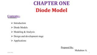
- 1. CHAPTER ONE Diode Model Prepared By: Muhabaw A. 18-04-2022 1 Contents:- Introduction Diode Models Modeling & Analysis Design and development stage Applications
- 2. 18-04-2022 2 INTRODUCTION TO DIODE A diode is a two-terminal semiconductor device. It offers a low resistance on the order of milli ohms in one direction and a high resistance on the order of giga ohms in the other direction. Thus a diode permits an easy current flow in only one direction. A diode exhibits a nonlinear relation between the voltage across its terminals and the current through it. However, analysis of a diode can be greatly simplified with the assumption of an ideal characteristic. Models are commonly used in evaluating the performance of diode circuits. If better accuracy is required, however, computer-aided modeling and simulation are normally used. It is the basic building block for many electronic circuits and systems.
- 3. 18-04-2022 3 Ideal Diodes:- Diode is a two terminals are the anode and the cathode. If the anode voltage is held positive with respect to the cathode terminal, the diode conducts and offers a small forward resistance. The diode is then said to be forward biased, and it behaves as a short circuit, as shown in Fig. 1.1(b). (a) Diode (b) Diode on (c) Diode off (d) Ideal v-i characteristic figure1.1:- Characteristics of an ideal diode
- 4. 18-04-2022 4 If the anode voltage is kept negative with respect to the cathode terminal, the diode offers a high resistance. The diode is then said to be reverse biased, and it behaves as an open circuit, as shown in Fig. 1.1(c). Thus, An ideal diode will offer zero resistance and zero voltage drop in the forward direction and. In the reverse direction, it will offer infinite resistance and allow zero current. An ideal diode behaves as a short circuit in the forward region of conduction (𝒗𝑫 = 𝟎) and as an open circuit in the reverse region of non conduction (𝒊𝑫 = 𝟎). The v-i characteristic of an ideal diode is shown in Fig. 1.1(d). Because the forward voltage tends to be greater than zero, the forward current through the diode tends to be infinite.
- 5. 18-04-2022 5 Example 1.1:- A diode circuit that can generate an OR logic function is shown in Fig. 1.2. A positive logic convention denotes logic 0 for 0 V and logic 1 for a positive voltage, typically 5 V. Show the truth table that illustrates the logic output. Figure1.2 Diode OR logic circuit Voltages Logic Levels 𝑉𝐴(v) 𝑉𝐵(v) 𝑉𝐶(v) A B C 0 0 0 0 0 0 0 5 4.3 0 1 1 5 0 4.3 1 0 1 5 5 4.3 1 1 1 NB:-If either 𝑉𝐴 or 𝑉𝐵 (or both) is high (+5V), the corresponding diode (𝐷1 or 𝐷2 or both) will conduct, and the output voltage will be high at 𝑉𝐶 = 5 V. A real diode has a finite voltage drop of approximately 0.7 V, and the output voltage will be approximately 5 - 0.7 = 4.3 V
- 6. 18-04-2022 6 Practical Diodes characteristics The characteristic of a practical diode that distinguishes it from an ideal one is that the practical diode experiences a finite voltage drop when it conducts. This drop is typically in the range of 0.5 V to 0.7 V. If the input voltage to a diode circuit is high enough, this small drop can be ignored. The voltage drop may, however, cause a significant error in electronic circuits. Voltage-versus-current (v-i) characteristic: 𝒊𝑫 = 𝑰𝒔(𝒆 𝒗𝑫 𝒏𝒗𝑻 − 𝟏) [1.1] Where 𝒊𝑫= current through the diode 𝒗𝑫 = diode voltage with the anode positive with respect to the cathode
- 7. 18-04-2022 7 𝑰𝒔 = leakage (or reverse saturation) current, typically in the range of 10−6 A to 10−15 A n = empirical constant known as the emission coefficient or the ideality factor, whose value varies from 1 to 2 Figure 1.3: voltage-versus-current characteristic of practical diode
- 8. 18-04-2022 8 The emission coefficient n depends on the material and the physical construction of the diode. For germanium diodes, n is considered to be 1. For silicon diodes, the predicted value of n is 2 at very small or large currents; but for most practical silicon diodes, the value of n falls in the range of 1.1 to 1.8. where q = electron charge 1.6022 * 10−19coulomb (C) 𝑽𝑻= is a constant called thermal voltage 𝑻𝒌= absolute temperature in kelvins 273+ 𝑇Celsius 𝒌 = Boltzmann’s constant 1.3806 *10−23 J per kelvin NB:- At a specific temperature, the leakage current 𝐼𝑠 will remain constant for a given diode. For small signal (low-power) diodes, the typical value of 𝑰𝒔 = 𝟏𝟎−𝟗 A 𝑽𝑻 = 𝒌𝑻𝒌 𝒒 = 25.8 mV,
- 9. 18-04-2022 9 Diodes can divided in to three based on its characteristics in figure 1.3 Forward-biased region:- 𝑽𝑫 > 𝟎 The diode current 𝐢𝐃 will be very small if the diode voltage 𝑽𝐃 is less than a specific value 𝑽𝑻𝐃, known as the threshold voltage. The diode conducts fully if 𝑽𝐃 is higher than 𝑽𝑻𝐃. Thus, the threshold voltage is the voltage at which a forward-biased diode begins to conduct fully. Example 1.2:- let is a small forward voltage 𝑽𝐃= 0.1 V is applied to a diode of n = 1 at room temperature. Then find the diode current 𝒊𝐃? 𝒊𝑫 = 𝑰𝒔 𝒆 𝒗𝑫 𝒏𝒗𝑻 − 𝟏 ≈ 𝑰𝒔 𝒆 𝒗𝑫 𝒏𝒗𝑻 Solution:- 𝒊𝑫 = 𝑰𝒔(𝒆 𝒗𝑫 𝒏𝒗𝑻 − 𝟏) = 𝑰𝒔 𝒆 𝟎.𝟏 𝟏𝒙 𝟎.𝟎𝟐𝟓𝟖 − 𝟏 = 𝑰𝒔(48.23 -1 ) = 47.23𝑰𝒔 NB:-when, 𝑽𝐃 > 0.1 V & 𝒊𝑫>>𝑰𝑺, it can be approximated within 2.1% error by
- 10. 18-04-2022 10 Reverse-Biased Region:- In the reverse-biased region, 𝑽𝑫 < 0. That is, 𝑽𝑫 is negative. If |𝑽𝑫| >> 𝑽𝑻, which occurs for 𝑽𝑫 < - 0.1V, so the exponential term becomes negligibly small compared to unity, and the diode current 𝒊𝑫becomes 𝒊𝑫 = 𝑰𝒔 𝒆 −|𝒗𝑫| 𝒏𝒗𝑻 − 𝟏 ≈ - 𝑰𝒔 Which indicates that the diode current 𝒊𝑫 remains constant in the reverse direction and is equal to 𝑰𝑺 in magnitude. Breakdown Region :- The reverse voltage is high—usually greater than 100 V. If the magnitude of the reverse voltage exceeds a specified voltage known as the breakdown voltage 𝑽BR , the corresponding reverse current 𝑰𝑩𝑽 Power dissipation 𝑷𝑫 = 𝑽𝑫𝒊𝑫 [1.2]
- 11. 18-04-2022 11 Determination of Diode Constants Diode constants 𝑰𝒔 and n can be determined either from experimentally measured v-i data or from the v-i characteristic. Taking the natural (base e) logarithm of both sides of Eq. (1.1), 𝐥𝐧 𝒊𝑫 = 𝒍𝒏 𝑰𝑺 + 𝑽𝑫 𝒏𝑽𝑻 which, after simplification, gives the diode voltage 𝑉𝐷 as 𝑽𝑫 = 𝒏𝑽𝑻 𝒍𝒏(𝒊𝑫/𝑰𝑺) [1.3] If we convert the natural log of base e to the logarithm of base 10, Eq. (1.3) becomes 𝑽𝑫 = 𝟐. 𝟑𝒏𝑽𝑻 𝐥𝐨𝐠(𝒊𝑫/𝑰𝑺) [1.4] Which indicates that the diode voltage 𝑉𝐷 is a nonlinear function of the diode current 𝑖𝐷.
- 12. 18-04-2022 12 If 𝑉𝐷1 is the diode voltage corresponding to diode current 𝑖𝐷1, Eq. (1.3) gives 𝑽𝑫𝟏 = 𝒏𝑽𝑻 𝒍𝒏(𝒊𝑫𝟏/𝑰𝑺) [1.5] Similarly, if 𝑉𝐷2 is the diode voltage corresponding to the diode current 𝑖𝐷2, we get 𝑽𝑫𝟐 = 𝒏𝑽𝑻 𝒍𝒏(𝒊𝑫𝟐/𝑰𝑺) [1.6] Therefore, the difference in diode voltages can be expressed by 𝑽𝑫𝟐 − 𝑽𝑫𝟏 = 𝒏𝑽𝑻 𝒍𝒏(𝒊𝑫𝟐/𝑰𝑺)- 𝒏𝑽𝑻 𝒍𝒏(𝒊𝑫𝟏/𝑰𝑺) = 𝒏𝑽𝑻 𝒍𝒏(𝒊𝑫𝟐/𝒊𝑫𝟏) [1.7] which can be converted to the logarithm of base 10 as 𝑽𝑫𝟐 − 𝑽𝑫𝟏 = 𝟐. 𝟑𝒏𝑽𝑻 𝐥𝒐𝒈(𝒊𝑫𝟐/𝒊𝑫𝟏) [1.8] This shows that for a decade (i.e., a factor of 10) change in diode current 𝑖𝐷2 = 10𝑖𝐷1, the diode voltage will change by 2.3n𝑉𝑇.
- 13. 18-04-2022 13 Thus, Eq. (1.3) can be written as 𝑽𝑫 = 𝟐. 𝟑𝒏𝑽𝑻 𝒍𝒐𝒈(𝒊𝑫) − 𝟐. 𝟑𝒏𝑽𝑻 𝒍𝒐𝒈(𝒊𝑺) [1.9] The equation has similar equation with y = mx - c where c=2.3𝑛𝑉𝑇 log(𝐼𝑆) and m = 2.3𝑛𝑉𝑇 per decade of current. The values of 𝐼𝑆 and n can be calculated as follows: Plot 𝑉𝐷 against 𝑖𝐷 on a semi-log scale, 𝑉𝐷 in the linear scale and 𝑖𝐷 in the log scale. Figure 1.4 diode v-i characteristic plotted on a semi-log scale
- 14. 18-04-2022 14 Find the slope m per decade of current change on the 𝑉𝐷-axis and find the emission coefficient n for the known value of slope m—that is, 𝒏 = 𝒎 𝟐. 𝟑𝑽𝑻 = 𝒎 𝟐. 𝟑 ∗ 𝟎. 𝟎𝟎𝟐𝟓𝟖 Example 1.3: The measured values of a diode at a junction temperature of 25°C are given by 𝑉𝐷 = 0.5𝑉 𝑎𝑡 𝑖𝐷 = 5𝜇𝐴 0.6𝑉 𝑎𝑡 𝑖𝐷 = 100𝜇𝐴 Determine (a) the emission coefficient n and (b) the leakage current 𝐼𝑆.
- 15. 18-04-2022 15 Temperature Effects The leakage current 𝐼𝑆 depends on the junction temperature 𝑇𝑗 (in Celsius) and increases at the rate of approximately +7.2% per degree Celsius for silicon and germanium diodes. Thus, by adding the increments for each degree rise in the junction temperature up to 10°C, we get 𝐼𝑆(𝑇𝑗 = 10) = 𝐼𝑆 [1 + 0.072 + (0.072 +0.0722 ) + (0.0722 + 0.0723 ) +(0.0723 + 0.0724 ) + 0.0724 + 0.0725 + 0.0725 + 0.0726 + 0.0726 + 0.0727 + 0.0727 + 0.0728 + 0.0728 + 0.0729 +(0.0729 + 0.07210 )] ≈ 2𝐼𝑆 That is, 𝐼𝑆 approximately doubles for every 10°C increase in temperature and can be related to any temperature change by
- 16. 18-04-2022 16 𝐼𝑆(𝑇𝑗)=𝐼𝑆(𝑇𝑜)*2(𝑇𝑗−𝑇𝑜)/10 = 𝐼𝑆(𝑇𝑜)*20.1(𝑇𝑗−𝑇𝑜) Where 𝐼𝑆(𝑇𝑜)is the leakage current at temperature 𝑇𝑜. Substituting 𝑉𝑇 = 𝐾𝑇𝐾/𝑞 in Eq. (1.3) gives the temperature dependence of the forward diode voltage. That is, 𝑉𝐷 = 𝑛𝐾(273+𝑇𝑗) 𝑞 ln(𝑖𝐷/𝐼𝑆) [1.10] Which, after differentiation of 𝑉𝐷 with respect to 𝑇𝑗, gives 𝜕𝑉𝐷 𝜕𝑇𝑗 = 𝑛𝑘 𝑞 ln(𝑖𝐷/𝐼𝑆) − 𝑛𝑘 273+𝑇𝑗 𝑞𝐼𝑆 𝜕𝐼𝑆 𝜕𝑇𝑗 = 𝑉𝐷 273+𝑇𝑗 − 𝑛𝑉𝑇 𝐼𝑆 𝜕𝐼𝑆 𝜕𝑇𝑗 [1.11] At a given diode current 𝑖𝐷, the diode voltage 𝑉𝐷 decreases with the temperature. The threshold voltage 𝑉𝑇𝐷 also depends on the temperature 𝑇𝑗. As the temperature increases, 𝑉𝑇𝐷 decreases 𝑉𝑇𝐷(𝑇𝑗) = 𝑉𝑇𝐷(𝑇0) + 𝐾𝑇𝐶(𝑇𝑗-𝑇0) [1.12]
- 17. 18-04-2022 17 Where 𝑇0 =junction temperature at 25°C 𝑇𝑗 = new junction temperature, in °C 𝑉𝑇𝐷(𝑇0) = threshold voltage at junction temperature 𝑇0 𝑉𝑇𝐷(𝑇𝑗) = threshold voltage at new junction temperature 𝑇𝑗 𝐾𝑇𝐶 = temperature coefficient, in V/°C Diode type 𝑉𝑇𝐷(𝑇0) 𝐾𝑇𝐶(V/°C ) silicon 0.7V -2m germanium 0.3V -2.5m Schottky 0.3V -1.5m Table1.1:-Threshold voltage and temperature coefficients of a different diodes Example 1.4:The threshold voltage 𝑉𝑇𝐷 of a silicon diode is 0.7 V at 25°C. Find the threshold voltage 𝑉𝑇𝐷 at (a) 𝑇𝑗= 100°C and (b) 𝑇𝑗= -100°C.
- 18. 18-04-2022 18 Analysis of Practical Diode Circuits A diode is used as a part of an electronic circuit, and the diode current 𝑖𝐷 becomes dependent on other circuit elements. A simple diode circuit is shown in Fig. 1.5. Applying Kirchhoff’s voltage law (KVL), we can express the source voltage 𝑉𝑆 and the diode current 𝑖𝐷 by Figure 1.5 simple diode circuit 𝑉𝑆= 𝑉𝐷 + 𝑅𝐿𝑖𝐷 Which gives the diode current 𝑖𝐷 as 𝑖𝐷 = 𝑉𝑆−𝑉𝐷 𝑅𝐿 [1.13] approximate method Example 1.5: find a current of silicon diode at 10V source with 1KΩ load?, then find 𝑉𝐷𝑛𝑒𝑤 if 𝐼𝑆 = 2.682 ∗ 10−9A & n =1.84 NB: default value of 𝑽𝑫=𝑽𝑻𝑫
- 19. 18-04-2022 19 Modeling of Practical Diodes To simplify the analysis and design of diode circuits, a diode can represent on the following models: A. constant-drop DC model B. piecewise linear DC model C. low-frequency AC model D. high-frequency AC model E. SPICE diode model.
- 20. 18-04-2022 20 A. Constant-Drop DC Model:- A conducting diode has a voltage drop 𝑉𝐷 that remains almost constant and is independent of the diode current. That is, 𝑉𝐷 = 𝑉𝑇𝐷 𝑉𝐷 = 𝑉𝑇𝐷, 𝑓𝑜𝑟 𝑉𝐷 ≥ 𝑉𝑇𝐷 0, 𝑓𝑜𝑟 𝑉𝐷 < 𝑉𝑇𝐷 Figure 1.6 constant-drop dc model 𝑖𝐷 can be determined 𝑖𝐷 = 𝑉𝑆−𝑉𝑇𝐷 𝑅𝐿
- 21. 18-04-2022 21 B. Piecewise Linear DC Model: The voltage drop across a practical diode increases with its current. Figure 1.7 piecewise linear dc model 𝑅𝐷 = ∆𝑉𝐷 ∆𝑖𝐷 at Q−point = 𝑉𝑋 − 𝑉𝑇𝐷 𝑖𝑋 𝑖𝑋 = 𝑖𝐷(𝑚𝑎𝑥) = 𝑉𝑆 𝑅𝐿 By applying KVL 𝑉𝑆 = 𝑉𝑇𝐷 + 𝑅𝐷𝑖𝐷 + 𝑅𝐿𝑖𝐷 Which gives the diode current 𝑖𝐷 as 𝑖𝐷 = 𝑉𝑆 − 𝑉𝑇𝐷 𝑅𝐷 + 𝑅𝐿
- 22. 18-04-2022 22 Reading assignment Low-frequency AC model High-frequency AC model SPICE diode model Tabular Representation
- 23. 18-04-2022 23 Zener Diodes A diode especially designed to have a steep characteristic in the breakdown region is called a Zener diode. Figure 1.8 characteristic of Zener diodes
- 24. 18-04-2022 24 A diode especially designed to have a steep characteristic in the breakdown region is called a Zener diode. The symbol for a Zener diode is shown in Fig. 1.8(a), and its v-i characteristic appears in Fig. 1.8(b). 𝑉𝑍𝐾 is the knee voltage, and 𝐼𝑍𝐾 is its corresponding current. A Zener diode is specified by its breakdown voltage, called the Zener voltage (or reference voltage) 𝑉𝑍, at a specified test current 𝑰𝒁= 𝑰𝒁𝑻. 𝑰𝒁(max) is the maximum current that the Zener diode can withstand and still remain within permissible limits for power dissipation. 𝑰𝒁(min) is the minimum current, slightly below the knee of the characteristic curve, at which the diode exhibits the reverse breakdown. That is, 𝑰𝒁(min) = 𝑰𝒁𝑲.
- 25. 18-04-2022 25 The reverse (Zener) characteristic of Fig. 1.8(b) can be approximated by a piecewise linear model with a fixed voltage 𝑉𝑍𝑂 and an ideal diode in series with resistance 𝑅𝑍. The equivalent circuit of the Zener action is shown in Fig. 1.8(d) for |𝑉𝐷| >𝑉𝑍. 𝑅𝑍 depends on the inverse slope of the Zener characteristic and is defined as 𝑅𝑍 = ∆𝑉𝑍 𝑖𝑍 𝑎𝑡𝑉𝑍 = ∆𝑉𝐷 ∆𝑖𝐷 𝑎𝑡𝑉𝐷 < 0 𝑎𝑛𝑑𝑖𝐷 < 0 𝑅𝑍 is also called the Zener resistance. The value of 𝑅𝑍 remains almost constant over a wide range of the Zener characteristic. The Zener current 𝑖𝑍 ( =-𝑖𝐷) can be related to 𝑉𝑍𝑂 and 𝑅𝑍 by 𝑉𝑍 = 𝑉𝑍𝑂 + 𝑅𝑍𝑖𝑍
- 26. 18-04-2022 26 Zener Regulator The value of 𝑅𝑍 is very small. Thus, the Zener voltage 𝑉𝑍 is almost independent of the reverse diode current 𝑖𝐷 = −𝑖𝑍. Because of the constant voltage characteristic in the breakdown region, a Zener diode can be employed as a voltage regulator. A regulator maintains an almost constant output voltage even though the DC supply voltage and the load current may vary over a wide range. A Zener voltage regulator is also known as a shunt regulator because the Zener diode is connected in shunt (or parallel) with the load 𝑅𝐿. If the Zener diode is replaced by its piecewise linear model with 𝑉𝑍𝑂 and 𝑅𝑍, the equivalent circuit shown in Fig. 1.9(b) is created.
- 27. 18-04-2022 27 Figure 1.9 Zener shunt regulator The output voltage is defined by a factor called the line regulation, which is related to 𝑅𝑆 and 𝑅𝑍: Line regulation = ∆𝑉𝑂 ∆𝑉𝑆 = 𝑅𝑍 𝑅𝑍+𝑅𝑆 and Load regulation = ∆𝑉𝑂 ∆𝑖𝐿 = −(𝑅𝑍||𝑅𝑆)
- 28. 18-04-2022 28 Any change in the Zener voltage 𝑉𝑍𝑂 will increase the output voltage. The variation of the output voltage is defined by a factor called the Zener regulation, which is related to 𝑅𝑆 and 𝑅𝑍: Zener regulation = ∆𝑉𝑂 ∆𝑉𝑍𝑂 = 𝑅𝑍 𝑅𝑍+𝑅𝑆 Thus, applying the superposition theorem, we can find the effective output voltage 𝑉𝑂 of the regulator in fig. 1.9(b) as follows: 𝑉𝑂 = ∆𝑉𝑂 ∆𝑉𝑍𝑂 ∆𝑉𝑍𝑂 + ∆𝑉𝑂 ∆𝑉𝑆 ∆𝑉𝑆 + ∆𝑉𝑂 ∆𝑖𝐿 ∆𝑖𝐿 = 𝑅𝑆 𝑅𝑍+𝑅𝑆 ∆𝑉𝑍𝑂 + 𝑅𝑍 𝑅𝑍+𝑅𝑆 ∆𝑉𝑆 − (𝑅𝑍||𝑅𝑆)∆𝑖𝐿 [1.14] Read Example 4.12 on your text book!!!!
- 29. 18-04-2022 29 Design of a Zener Regulator If 𝑖𝑍 is the Zener current and 𝑖𝐿 is the load current, the value of resistance 𝑅𝑆 can be found from The regulator must be designed to do the following: 1. To ensure that the Zener current will exceed 𝑖𝑍 (min) when the supply voltage is minimum 𝑉𝑆 (min) and the load current is maximum 𝑖𝐿 (max). Applying Eq. (1.15), we can find 𝑅𝑆 from [1.15] [1.16]
- 30. 18-04-2022 30 2. To ensure that the Zener current will not exceed 𝑖𝑍 (max) when the supply voltage is maximum 𝑉𝑆 (max) and the load current is minimum 𝑖𝐿 (min). Using Eq. (1.15), we can find 𝑅𝑆 from [1.17] Equating 𝑅𝑆 in Eq. (1.16) to 𝑅𝑆 in Eq. (1.17), we get the relationship of the maximum Zener current in terms of the variations in 𝑉𝑆 and 𝑖𝐿. That is, (𝑉𝑆 (min) -𝑉𝑍𝑂 − 𝑅𝑍𝑖𝑍 (min)) 𝑖𝑍 (max) + 𝑖𝐿 (min) = (𝑉𝑆 (max) -𝑉𝑍𝑂 − 𝑅𝑍𝑖𝑍 (max)) 𝑖𝑍 (min) + 𝑖𝐿 (max) [1.18]
- 31. 18-04-2022 31 The minimum Zener current 𝑖𝑍 (min) is normally limited to 10% of the maximum Zener current 𝑖𝑍 (max) to ensure operation in the breakdown region. That is, 𝑖𝑍 (min) =0.1 * 𝑖𝑍 (max) Read example 4.13 on your text book!!!
- 32. 18-04-2022 32 Some Common Applications of Diodes Some list of common applications of diodes Rectifiers Clipper Circuits Clamping Circuits Reverse Current Protection Circuits In Logic Gates Voltage Multipliers
- 33. 18-04-2022 33
Editor's Notes
- Type equation here.