Downloaded 703 times
![Institute Of Engineering Studies (IES,Bangalore)
Formulae Sheet in ECE/TCE Department
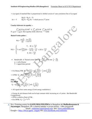
Communication Systems
Amplitude Modulation :
DSB-SC :
u (t) =
m(t) cos 2π t
Power P =
Conventioanal AM :
u (t) = [1 + m(t)] Cos 2π t . as long as |m(t)| ≤ 1 demodulation is simple .
Practically m(t) = a m (t) .
()
()
Modulation index a = ( ) , m (t) =
| ( )|
Power =
+
SSB-AM :
→ Square law Detector SNR =
()
Square law modulator
↓
= 2a / a → amplitude Sensitivity
Envelope Detector R C (i/p) < < 1 /
R C (o/P) >> 1/
R C << 1/ω
≥
Frequency & Phase Modulation : Angle Modulation :u (t) =
∅ (t)
Cos (2π t + ∅ (t) )
( ) →
2π
phase & frequency deviation constant
m(t) . dt →
→ max phase deviation ∆∅ =
max | m(t) |
→ max requency deviation ∆ = max |m(t) |
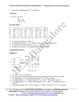
Bandwidth :
Effective Bandwidth
= 2 (β + 1)
→ 98% power
Noise in Analog Modulation :→ (SNR)
R = m(t) cos 2π
1
=
=
=
∴
=
/2
No.1 Training center for GATE/IES/JTO/PSUs in Bangalore @ Malleshwaram &
Jayanagar, Bangalore. Ph: 0 99003 99699/ 0 97419 00225 / 080-32552008
Email : onlineies.com@gmail.com Site: www.onlineIES.com
Google+: http://bit.ly/gplus_iesgate FB: www.facebook.com/onlineies](https://image.slidesharecdn.com/eceformulasheet-140115235452-phpapp01/85/Ece-formula-sheet-1-320.jpg)
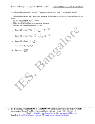
![Institute Of Engineering Studies (IES,Bangalore)
→ (SNR)
=
/
→ (SNR)
=
/
=
/
/
=
=
=
.
=
=
=
=
= (SNR)
= (SNR)
= η
Formulae Sheet in ECE/TCE Department
.
η=
Noise in Angle Modulation :-
=
PCM :→ Min. no of samples required for reconstruction = 2ω =
→ Total bits required = v
→ Bandwidth = R /2 = v
; ω = Bandwidth of msg signal .
bps . v → bits / sample
/2=v.ω
→ SNR = 1.76 + 6.02 v
→ As Number of bits increased SNR increased by 6 dB/bit . Band width also increases.
Delta Modulation :→ By increasing step size slope over load distortion eliminated [ Signal raised sharply ]
→ By Reducing step size Grannualar distortion eliminated . [ Signal varies slowly ]
Digital Communication
Matched filter:
→ impulse response a(t) =
( T – t) . P(t) → i/p
→ Matched filter o/p will be max at multiples of ‘T’ . So, sampling @ multiples of ‘T’ will give max SNR
(2nd point )
→ matched filter is always causal a(t) = 0 for t < 0
→ Spectrum of o/p signal of matched filter with the matched signal as i/p ie, except for a delay factor ;
proportional to energy spectral density of i/p.
∅ ()=
(f) ∅(f) = ∅(f) ∅*(f) e
∅ ( ) = |∅( )| e
2
No.1 Training center for GATE/IES/JTO/PSUs in Bangalore @ Malleshwaram &
Jayanagar, Bangalore. Ph: 0 99003 99699/ 0 97419 00225 / 080-32552008
Email : onlineies.com@gmail.com Site: www.onlineIES.com
Google+: http://bit.ly/gplus_iesgate FB: www.facebook.com/onlineies](https://image.slidesharecdn.com/eceformulasheet-140115235452-phpapp01/85/Ece-formula-sheet-2-320.jpg)
![Institute Of Engineering Studies (IES,Bangalore)
Formulae Sheet in ECE/TCE Department
Signals & Systems
→ Energy of a signal
| [ ]|
|x(t)| dt =
→ Power of a signal P = lim
→ x (t) →
; x (t) →
x (t) + x (t) → +
|x(t)| dt = lim
→
→
|x[n]|
iff x (t) & x (t) orthogonal
→ Shifting & Time scaling won’t effect power . Frequency content doesn’t effect power.
→ if power = ∞ → neither energy nor power signal
Power = 0 ⇒ Energy signal
Power = K ⇒ power signal
→ Energy of power signal = ∞ ; Power of energy signal = 0
→ Generally Periodic & random signals → Power signals
Aperiodic & deterministic → Energy signals
Precedence rule for scaling & Shifting :
x(at + b) → (1) shift x(t) by ‘b’ → x(t + b)
(2) Scale x(t + b) by ‘a’ → x(at + b)
x( a ( t + b/a)) → (1) scale x(t) by a → x(at)
(2) shift x(at) by b/a → x (a (t+b/a)).
→ x(at +b) = y(t) ⇒ x(t) = y
Step response s(t) = h(t) * u(t) =
S[n] =
[ ]
e
Rect (t / 2T) * Rect (t / 2T) = 2T tri(t / T)
h(t)dt
S’ (t) = h(t)
h[n] = s[n] – s[n-1]
u(t) * e
u(t) =
[e
- e ] u(t) .
Rect (t / 2 ) *
Rect(t / 2 ) = 2
min ( ,
) trapezoid ( ,
)
Hilbert Transform Pairs :
e
/
dx = σ 2π ;
x e
/
dx = σ
2π σ > 0
Laplace Transform :-
5
No.1 Training center for GATE/IES/JTO/PSUs in Bangalore @ Malleshwaram &
Jayanagar, Bangalore. Ph: 0 99003 99699/ 0 97419 00225 / 080-32552008
Email : onlineies.com@gmail.com Site: www.onlineIES.com
Google+: http://bit.ly/gplus_iesgate FB: www.facebook.com/onlineies](https://image.slidesharecdn.com/eceformulasheet-140115235452-phpapp01/85/Ece-formula-sheet-5-320.jpg)
![Institute Of Engineering Studies (IES,Bangalore)
Formulae Sheet in ECE/TCE Department
(s) e ds
x(t) =
x(t) e
X(s) =
ds
Initial & Final value Theorems :
x(t) = 0 for t < 0 ; x(t) doesn’t contain any impulses /higher order singularities @ t =0 then
x(
) = lim
x(∞) = lim
( )
→
→
( )
Properties of ROC :1. X(s) ROC has strips parallel to jω axis
2. For rational laplace transform ROC has no poles
3. x(t) → finite duration & absolutely integrable then ROC entire s-plane
4. x(t) → Right sided then ROC right side of right most pole excluding pole s = ∞
5. x(t) → left sided
ROC left side of left most pole excluding s= - ∞
6. x(t) → two sided
ROC is a strip
7. if x(t) causal
ROC is right side of right most pole including s = ∞
8. if x(t) stable
ROC includes jω-axis
Z-transform :x[n] =
X(z) =
x( )
dz
x[n]
Initial Value theorem :
If x[n] = 0 for n < 0 then x[0] = lim
Final Value theorem :lim→ [ ] = lim → (
→
( )
1) X(z)
Properties of ROC :1.ROC is a ring or disc centered @ origin
2. DTFT of x[n] converter if and only if ROC includes unit circle
3. ROC cannot contain any poles
6
No.1 Training center for GATE/IES/JTO/PSUs in Bangalore @ Malleshwaram &
Jayanagar, Bangalore. Ph: 0 99003 99699/ 0 97419 00225 / 080-32552008
Email : onlineies.com@gmail.com Site: www.onlineIES.com
Google+: http://bit.ly/gplus_iesgate FB: www.facebook.com/onlineies](https://image.slidesharecdn.com/eceformulasheet-140115235452-phpapp01/85/Ece-formula-sheet-6-320.jpg)
![Institute Of Engineering Studies (IES,Bangalore)
Formulae Sheet in ECE/TCE Department
4. if x[n] is of finite duration then ROC is enter Z-plane except possibly 0 or ∞
5. if x[n] right sided then ROC → outside of outermost pole excluding z = 0
6. if x[n] left sided then ROC → inside of innermost pole including z =0
7. if x[n] & sided then ROC is ring
8. ROC must be connected region
9.For causal LTI system ROC is outside of outer most pole including ∞
10.For Anti Causal system ROC is inside of inner most pole including ‘0’
11. System said to be stable if ROC includes unit circle .
12. Stable & Causal if all poles inside unit circle
13. Stable & Anti causal if all poles outside unit circle.
Phase Delay & Group Delay :When a modulated signal is fixed through a communication channel , there are two different delays to be
considered.
(i) Phase delay:
Signal fixed @ o/p lags the fixed signal by ∅(ω ) phase
∅( )
=where ∅(ω ) = K H(jω)
Group delay
∅(
=
↓
Frequency response of channel
)
for narrow Band signal
↓
Signal delay / Envelope delay
Probability & Random Process:→ P (A/B) =
(
)
( )
→ Two events A & B said to be mutually exclusive /Disjoint if P(A B) =0
→ Two events A & B said to be independent if P (A/B) = P(A) ⇒ P(A B) = P(A) P(B)
→ P(Ai / B) =
(
)
( )
=
CDF :Cumulative Distribution function
(
)
(
)
(x) = P { X ≤ x }
Properties of CDF :
(∞) = P { X ≤ ∞ } = 1
(- ∞) = 0
(x ≤ X ≤ x ) = (x ) - (x )
Its Non decreasing function
P{ X > x} = 1 – P { X ≤ x} = 1- (x)
PDF :Pdf =
7
(x) =
(x)
No.1 Training center for GATE/IES/JTO/PSUs in Bangalore @ Malleshwaram &
Jayanagar, Bangalore. Ph: 0 99003 99699/ 0 97419 00225 / 080-32552008
Email : onlineies.com@gmail.com Site: www.onlineIES.com
Google+: http://bit.ly/gplus_iesgate FB: www.facebook.com/onlineies](https://image.slidesharecdn.com/eceformulasheet-140115235452-phpapp01/85/Ece-formula-sheet-7-320.jpg)
![Institute Of Engineering Studies (IES,Bangalore)
a -
E=
(
Formulae Sheet in ECE/TCE Department
)
a .
‘E’ due to volume charge E =
→ Electric flux density D =
Flux Ψ = s .
D → independent of medium
Gauss Law :→ Total flux coming out of any closed surface is equal to total charge enclosed by surface .
Ψ=
⇒ D . ds =
= ρ . dv
ρ = .D
→ Electric potential
=
a . dr a =
=
. d (independent of path)
= -
-
(for point charge )
Potential @ any point (distance = r), where Q is located same where , whose position is vector @ r
V=
|
|
→ V(r) =
+ C . [ if ‘C’ taken as ref potential ]
→ × E = 0, E = - V
→ For monopole E ∝ ; Dipole E ∝
.
V∝ ;
V ∝
Electric lines of force/ flux /direction of E always normal to equipotential lines .
Energy Density
=
=
D. dv =
dv
Continuity Equation
ρ =ρ
e
/
.J = -
where
.
= Relaxation / regeneration time = /σ (less for good conductor )
Boundary Conditions :=
Tangential component of ‘E’ are continuous across dielectric-dielectric Boundary .
Tangential Components of ‘D’ are dis continues across Boundary .
=
;
= / .
Normal components are of ‘D’ are continues , where as ‘E’ are dis continues.
D - D =ρ ;
=
;
= =
=
=
=
t
=
Maxwell’s Equations :→ faraday law
=
.d = → Transformer emf =
14
.d = -
. ds
ds ⇒
×E=-
No.1 Training center for GATE/IES/JTO/PSUs in Bangalore @ Malleshwaram &
Jayanagar, Bangalore. Ph: 0 99003 99699/ 0 97419 00225 / 080-32552008
Email : onlineies.com@gmail.com Site: www.onlineIES.com
Google+: http://bit.ly/gplus_iesgate FB: www.facebook.com/onlineies](https://image.slidesharecdn.com/eceformulasheet-140115235452-phpapp01/85/Ece-formula-sheet-14-320.jpg)
![Institute Of Engineering Studies (IES,Bangalore)
α=0,β=ω
; u = 1/
Here also E & H in phase .
Formulae Sheet in ECE/TCE Department
, λ = 2π/β
Good Conductor :σ >>ω
σ/ω → ∞ ⇒ σ = ∞
=
η=
/
< = 12 π ∠
=
α = β = π σ ; u = 2ω/ σ ; λ = 2π / β ; η =
Skin depth δ = 1/α
η=
2e / =
Skin resistance R =
R
=
R
=
∠
=
.
.
Poynting Vector :(
) ds =
S
+
[
] dv – σ
v
δ
Total time avge power crossing given area
(z) =
| |
e
dv
cos
a
(s) ds
=
S
Direction of propagation :- (
a ×a =a
)
a ×a =a
→ Both E & H are normal to direction of propagation
→ Means they form EM wave that has no E or H component along direction of propagation .
Reflection of plane wave :(a) Normal incidence
Reflection coefficient Γ =
=
coefficient Τ =
=
Medium-I Dielectric , Medium-2 Conductor :>
:Γ
there is a standing wave in medium
Max values of | | occurs
= - nπ/β =
n = 1 2….
=
16
(
)
=
(
wave in medium ‘2’.
)
No.1 Training center for GATE/IES/JTO/PSUs in Bangalore @ Malleshwaram &
Jayanagar, Bangalore. Ph: 0 99003 99699/ 0 97419 00225 / 080-32552008
Email : onlineies.com@gmail.com Site: www.onlineIES.com
Google+: http://bit.ly/gplus_iesgate FB: www.facebook.com/onlineies](https://image.slidesharecdn.com/eceformulasheet-140115235452-phpapp01/85/Ece-formula-sheet-16-320.jpg)
![Institute Of Engineering Studies (IES,Bangalore)
Formulae Sheet in ECE/TCE Department
Stability & Biasing :- ( Should be as min as possible)
For S =
∆
∆
∆
S =
= S. ∆
+S ∆
∆
∆
S =
∆
∆
+ S ∆β
For fixed bias S =
Collector to Base bias S =
Self bias S =
R =
For thermal stability [
=1+β
0 < s < 1+ β =
≈ 1+
βR > 10 R
; R =
- 2 (R + R )] [ 0.07
. S] < 1/
;
<
Hybrid –pi(π)- Model :g =|
|/
r
= h /g
r =h -r
r =r /h
g = h - (1+ h ) g
For CE :
=
=h
(
)
=
(
;
)
=
C = C + C (1 + g R )
=
= S.C current gain Bandwidth product
= Upper cutoff frequency
For CC :
For CB:
=
22
≈
=
(
=
)
=
= (1 + h )
(
)
= (1 + β)
No.1 Training center for GATE/IES/JTO/PSUs in Bangalore @ Malleshwaram &
Jayanagar, Bangalore. Ph: 0 99003 99699/ 0 97419 00225 / 080-32552008
Email : onlineies.com@gmail.com Site: www.onlineIES.com
Google+: http://bit.ly/gplus_iesgate FB: www.facebook.com/onlineies](https://image.slidesharecdn.com/eceformulasheet-140115235452-phpapp01/85/Ece-formula-sheet-22-320.jpg)
![Institute Of Engineering Studies (IES,Bangalore)
=
>
Ebress moll model :=-α
+
(1- e
=-α
α
/
>
)
/
(1- e
+
Formulae Sheet in ECE/TCE Department
)
=α
Multistage Amplifiers :
* =
2 /
1 ;
.
Rise time t =
t = 1.1 t
+t
= 1.1
+
+
= 1.1
+
/
+
=
.
.
+
=
Differential Amplifier :
= h + (1 + h ) 2R = 2 h R ≈ 2βR
|
g =
|
CMRR =
= g of BJT/4
=
;
R ↑,→
Darlington Pair :
= (1 + β ) (1 + β ) ;
=
(
)
R =(
)
α → DC value of α
↑
↑
C RR ↑
≈ 1 ( < 1)
g = (1 + β ) g
Ω
[ if
&
have same type ] =
R
+
Tuned Amplifiers : (Parallel Resonant ckts used ) :
23
=
Q → ‘Q’ factor of resonant ckt which is very high
No.1 Training center for GATE/IES/JTO/PSUs in Bangalore @ Malleshwaram &
Jayanagar, Bangalore. Ph: 0 99003 99699/ 0 97419 00225 / 080-32552008
Email : onlineies.com@gmail.com Site: www.onlineIES.com
Google+: http://bit.ly/gplus_iesgate FB: www.facebook.com/onlineies](https://image.slidesharecdn.com/eceformulasheet-140115235452-phpapp01/85/Ece-formula-sheet-23-320.jpg)
![Institute Of Engineering Studies (IES,Bangalore)
B.W =
=
-
=
+
Formulae Sheet in ECE/TCE Department
/Q
∆
∆
For double tuned amplifier 2 tank circuits with same
used .
=
.
MOSFET (Enhancement) [ Channel will be induced by applying voltage]
NMOSFET formed in p-substrate
If
≥ channel will be induced & i (Drain → source )
→ +ve for NMOS
i ∝(
- ) for small
↑ → channel width @ drain reduces .
=
channel width ≈ 0 → pinch off further increase no effect
-
For every
i =
>
[(
there will be
-
)
-
→ triode region (
]
=
i =
r
[
=
(
24
[(
)
] → saturation
)
→ Drain to source resistance in triode region
→ induced channel
i =
-
C
PMOS : Device operates in similar manner except
,
,
i enters @ source terminal & leaves through Drain .
≤
<
) -
≥
]
→ Continuous channel
=
are –ve
C
≤
→ Pinched off channel .
NMOS Devices can be made smaller & thus operate faster . Require low power supply .
Saturation region → Amplifier
For switching operation Cutoff & triode regions are used
NMOS
PMOS
No.1 Training center for GATE/IES/JTO/PSUs in Bangalore @ Malleshwaram &
Jayanagar, Bangalore. Ph: 0 99003 99699/ 0 97419 00225 / 080-32552008
Email : onlineies.com@gmail.com Site: www.onlineIES.com
Google+: http://bit.ly/gplus_iesgate FB: www.facebook.com/onlineies](https://image.slidesharecdn.com/eceformulasheet-140115235452-phpapp01/85/Ece-formula-sheet-24-320.jpg)
![Institute Of Engineering Studies (IES,Bangalore)
≥
≤
Formulae Sheet in ECE/TCE Department
→ induced channel
-
>
-
<
→ Continuous channel(Triode region)
≥
-
≤
-
→ Pinchoff (Saturation)
Depletion Type MOSFET :- [ channel is physically implanted . i flows with
For n-channel
i -
Value of Drain current obtained in saturation when
→ +ve → enhances channel .
→ -ve → depletes channel
is –ve for n-channel
characteristics are same except that
∴
=0]
=
=0⇒
.
.
MOSFET as Amplifier :
For saturation
>
To reduce non linear distortion
i =
(
)
⇒
g =
)
(
)
=-g R
Unity gain frequency
JFET :
≤
≤
≤
=
(
)
⇒ i = 0 → Cut off
≤ 0,
≤
i
< < 2(
≤0 ,
=
2 1
≥
→ Triode
⇒
|
→ Saturation
|
|
|
Zener Regulators :
25
For satisfactory operation
≥
+
No.1 Training center for GATE/IES/JTO/PSUs in Bangalore @ Malleshwaram &
Jayanagar, Bangalore. Ph: 0 99003 99699/ 0 97419 00225 / 080-32552008
Email : onlineies.com@gmail.com Site: www.onlineIES.com
Google+: http://bit.ly/gplus_iesgate FB: www.facebook.com/onlineies](https://image.slidesharecdn.com/eceformulasheet-140115235452-phpapp01/85/Ece-formula-sheet-25-320.jpg)
![Institute Of Engineering Studies (IES,Bangalore)
Formulae Sheet in ECE/TCE Department
Power Amplifiers :
Fundamental power delivered to load
Total Harmonic power delivered to load
R
=
=
=
+
=
+
1+
R
..
+
+ ……
= [ 1+ D ]
Where D =
+D +
. . +D
D =
D = total harmonic Distortion .
Class A operation : o/p flows for entire
‘Q’ point located @ centre of DC load line i.e.,
=
/ 2 ; η = 25 %
Min Distortion , min noise interference , eliminates thermal run way
Lowest power conversion efficiency & introduce power drain
=
-i
if i = 0, it will consume more power
is dissipated in single transistors only (single ended)
Class B:
flows for 18 ; ‘Q’ located @ cutoff ; η = 78.5% ; eliminates power drain
Higher Distortion , more noise interference , introduce cross over distortion
Double ended . i.e ., 2 transistors .
= 0 [ transistors are connected in that way ]
=i
= 0.4
→ power dissipated by 2 transistors .
=i
Class AB operation :
flows for more than 18 & less than
‘Q’ located in active region but near to cutoff ; η = 60%
Distortion & Noise interference less compared to class ‘B’ but more in compared to class ‘A’
Eliminates cross over Distortion
Class ‘C’ operation :
flows for < 180 ; ‘Q’ located just below cutoff ; η = 87.5%
Very rich in Distortion ; noise interference is high .
Oscillators : For RC-phase shift oscillator f =
f=
27
h ≥ 4k + 23 +
where k = R /R
> 29
No.1 Training center for GATE/IES/JTO/PSUs in Bangalore @ Malleshwaram &
Jayanagar, Bangalore. Ph: 0 99003 99699/ 0 97419 00225 / 080-32552008
Email : onlineies.com@gmail.com Site: www.onlineIES.com
Google+: http://bit.ly/gplus_iesgate FB: www.facebook.com/onlineies](https://image.slidesharecdn.com/eceformulasheet-140115235452-phpapp01/85/Ece-formula-sheet-27-320.jpg)
![Institute Of Engineering Studies (IES,Bangalore)
Formulae Sheet in ECE/TCE Department
=
→ then Hermition
=
→ then Hermition
Diagonal elements of Skew Hermition Matrix must be purely imaginary or zero
Diagonal elements of Hermition matrix always real .
A real Hermition matrix is a symmetric matrix.
|KA| =
|A|
Eigen Values & Vectors : Char. Equation |A – λI| = 0.
Roots of characteristic equation are called eigen values . Each eigen value corresponds to non zero
solution X such that (A – λI)X = 0 . X is called Eigen vector .
Sum of Eigen values is sum of Diagonal elements (trace)
Product of Eigen values equal to Determinent of Matrix .
Eigen values of
& A are same
| |
λ is igen value o then 1/ λ →
&
is Eigen value of adj A.
λ , λ …… λ are Eigen values of A then
→
λ , K λ …….. λ
→ λ , λ ………….. λ .
A + KI
→ λ + k , λ + k , …….. λ + k
(
) → (λ
k) , ……… (λ
k)
Eigen values of orthogonal matrix have absolute value of ‘1’ .
Eigen values of symmetric matrix also purely real .
Eigen values of skew symmetric matrix are purely imaginary or zero .
λ , λ , …… λ distinct eigen values of A then corresponding eigen vectors
linearly independent set .
adj (adj A) = | |
; | adj (adj A) | = | |( )
,
, .. …
for
Complex Algebra :
Cauchy Rieman equations
Neccessary & Sufficient Conditions for f(z) to be analytic
30
( )/(
a)
f(z) = f( ) + ( )
dz =
(
)
[
(a) ] if f(z) is analytic in region ‘C’ & Z =a is single point
( )
(
)
(
)
+ …… + ( )
+ ………. Taylor Series
⇓
( )
if
= 0 then it is called Mclauren Series f(z) =
a (
) ; when a =
If f(z) analytic in closed curve ‘C’ except @ finite no. of poles then
+
No.1 Training center for GATE/IES/JTO/PSUs in Bangalore @ Malleshwaram &
Jayanagar, Bangalore. Ph: 0 99003 99699/ 0 97419 00225 / 080-32552008
Email : onlineies.com@gmail.com Site: www.onlineIES.com
Google+: http://bit.ly/gplus_iesgate FB: www.facebook.com/onlineies](https://image.slidesharecdn.com/eceformulasheet-140115235452-phpapp01/85/Ece-formula-sheet-30-320.jpg)
![Institute Of Engineering Studies (IES,Bangalore)
Formulae Sheet in ECE/TCE Department
( )d = 2πi (sum of Residues @ singular points within ‘C’ )
Res f(a) = lim
(
→
= Φ(a) /
= lim
( )
(a)
→ (
)
((
a) f(z) )
Calculus :Rolle’s theorem :If f(x) is
(a) Continuous in [a, b]
(b) Differentiable in (a, b)
(c) f(a) = f(b) then there exists at least one value C (a, b) such that
(c) = 0 .
Langrange’s Mean Value Theorem :If f(x) is continuous in [a, b] and differentiable in (a, b) then there exists atleast one value ‘C’ in (a, b)
such that
(c) =
( )
( )
Cauchy’s Mean value theorem :If f(x) & g(x) are two function such that
(a) f(x) & g(x) continuous in [a, b]
(b) f(x) & g(x) differentiable in (a, b)
(c) g (x) ≠ 0 ∀ x in (a, b)
Then there exist atleast one value C in (a, b) such that
(c) / g (c) =
( )
( )
( )
( )
Properties of Definite integrals :
31
(x). dx =
(x). dx +
a<c<b
(x)dx =
(a x)dx
(x). dx
No.1 Training center for GATE/IES/JTO/PSUs in Bangalore @ Malleshwaram &
Jayanagar, Bangalore. Ph: 0 99003 99699/ 0 97419 00225 / 080-32552008
Email : onlineies.com@gmail.com Site: www.onlineIES.com
Google+: http://bit.ly/gplus_iesgate FB: www.facebook.com/onlineies](https://image.slidesharecdn.com/eceformulasheet-140115235452-phpapp01/85/Ece-formula-sheet-31-320.jpg)
![Institute Of Engineering Studies (IES,Bangalore)
Formulae Sheet in ECE/TCE Department
Laplace Transform :
L
L { t f(t) } = ( 1)
( ) = s f(s) - s
()
⇔
f(0) - s
(0) ……
(0)
f(s)
(s) ds
(u) du ⇔ f(s) / s .
Inverse Transforms :
(
)
(
)
(
)
=
t sin at
=
[ sin at + at cos at]
=
[ sin at - at cos at]
= Cos hat
= Sin hat
Laplace Transform of periodic function : L { f(t) } =
()
Numerical Methods :Bisection Method :(1) Take two values of x & x such that f(x ) is +ve & f(x ) is –ve then x =
+ve then root lies between x & x otherwise it lies between x & x .
find f(x ) if f(x )
Regular falsi method :Same as bisection except x = x -
(
)
(
)
f(x )
Newton Raphson Method :x
=x –
( )
( )
Pi cards Method :-
33
No.1 Training center for GATE/IES/JTO/PSUs in Bangalore @ Malleshwaram &
Jayanagar, Bangalore. Ph: 0 99003 99699/ 0 97419 00225 / 080-32552008
Email : onlineies.com@gmail.com Site: www.onlineIES.com
Google+: http://bit.ly/gplus_iesgate FB: www.facebook.com/onlineies](https://image.slidesharecdn.com/eceformulasheet-140115235452-phpapp01/85/Ece-formula-sheet-33-320.jpg)
![Institute Of Engineering Studies (IES,Bangalore)
y
=y +
(x y )
←
Formulae Sheet in ECE/TCE Department
= f(x, y)
Taylor Series method := f(x, y)
y = y + (x- x ) (y ) +
(
)
(y) + ………….
(
)
+
)
(y)
Euler’s method :y = y + h f(x , y )
y
←
= f(x, y
( )
= y + [f(x , y ) + f(x + h, y )
( )
= y + [f(x , y ) + f(x
y
,y
( )
)]
:
:
Calculate till two consecutive value of ‘y’ agree
y = y + h f(x + h, y )
y
( )
= y + [f(x + h, y ) + f(x + 2h, y )
………………
Runge’s Method :k = h f(x , y )
k = h f( x + , y +
)
finally compute K = (
+4
+
finally compute K = (
+2
+2
)
k = h f(x +h , y + k )
k = h ( f (x +h , y + k ))
Runge Kutta Method :k = h f(x , y )
k = h f( x + , y +
34
)
No.1 Training center for GATE/IES/JTO/PSUs in Bangalore @ Malleshwaram &
Jayanagar, Bangalore. Ph: 0 99003 99699/ 0 97419 00225 / 080-32552008
Email : onlineies.com@gmail.com Site: www.onlineIES.com
Google+: http://bit.ly/gplus_iesgate FB: www.facebook.com/onlineies](https://image.slidesharecdn.com/eceformulasheet-140115235452-phpapp01/85/Ece-formula-sheet-34-320.jpg)
![Institute Of Engineering Studies (IES,Bangalore)
k = h f(x + , y +
Formulae Sheet in ECE/TCE Department
∴ approximation vale
)
y =y +K.
k = h f (x +h , y + k )
Trapezoidal Rule :(x). dx =
[ ( y + y ) + 2 (y + y + ……. y
)]
f(x) takes values y , y …..
@ x , x , x ……..
Simpson’s one third rule :(x). dx =
[ ( y + y ) + 4 (y + y + ……. y
) + 2 (y + y +
….+ y
)]
Simpson three eighth rule :(x). dx =
[ ( y + y ) + 3 (y + y + y + y + ……. y
)+ 2 (y + y +
….+ y
)]
Differential Equations :Variable & Seperable :f(y) dy = ϕ(x) dx
General form is
(y) dy = ϕ(x) dx + C .
Sol:
Homo generous equations :General form
=
(
(
⇒
Sol : Put y = Vx
)
)
f(x, y) & ϕ(x y) Homogenous of same degree
=V+x
& solve
Reducible to Homogeneous :General form
(i)
≠
Sol : Put
35
=
x=X+h
y=Y+k
No.1 Training center for GATE/IES/JTO/PSUs in Bangalore @ Malleshwaram &
Jayanagar, Bangalore. Ph: 0 99003 99699/ 0 97419 00225 / 080-32552008
Email : onlineies.com@gmail.com Site: www.onlineIES.com
Google+: http://bit.ly/gplus_iesgate FB: www.facebook.com/onlineies](https://image.slidesharecdn.com/eceformulasheet-140115235452-phpapp01/85/Ece-formula-sheet-35-320.jpg)
![Institute Of Engineering Studies (IES,Bangalore)
(
sin (ax + b) =
)
(
= x
(
f(- a ) = 0
sin (ax + b)
)
=x
( )
f(- a ) ≠ 0
sin (ax + b)
)
(
Formulae Sheet in ECE/TCE Department
Same applicable for cos (ax + b)
sin (ax + b)
)
x = [ (D)] x
( )
e
f(x) = e
(
f(x)
)
Vector Calculus :Green’s Theorem :(ϕ dx +
Ψ
x
dy) =
ϕ
y
dx dy
This theorem converts a line integral around a closed curve into Double integral which is special case of
Stokes theorem .
Series expansion :Taylor Series :f(x) = f(a) +
f(x) = f(0) +
( )
( )
x +
(1 + x) = 1+ nx +
e = 1+x+
( )
(x-a) +
(x
a) + …………+
( )
x + …………+
)
(x
a)
x + …… | nx| < 1
(
( )
( )
x
+ ……. (mc lower series )
+ ……..
Sin x = x -
+
- ……..
Cos x = 1 -
+
- ……..
Digital Electronics
37
Fan out of a logic gate =
Noise margin :
or
Power Dissipation
=
or
=
→
when o/p low
No.1 Training center for GATE/IES/JTO/PSUs in Bangalore @ Malleshwaram &
Jayanagar, Bangalore. Ph: 0 99003 99699/ 0 97419 00225 / 080-32552008
Email : onlineies.com@gmail.com Site: www.onlineIES.com
Google+: http://bit.ly/gplus_iesgate FB: www.facebook.com/onlineies](https://image.slidesharecdn.com/eceformulasheet-140115235452-phpapp01/85/Ece-formula-sheet-37-320.jpg)

This document contains formulas and concepts related to communication systems and signals and systems. It includes formulas for amplitude modulation techniques like DSB-SC, conventional AM, SSB-AM. It also includes formulas for frequency and phase modulation, PCM, delta modulation, digital modulation techniques like BPSK, FSK, PSK, and concepts like matched filters, probability, random variables, CDF, PDF and more. The document provides a comprehensive reference sheet of important formulas and concepts for communication systems and signals and systems.


![Ece ppt[1]](https://cdn.slidesharecdn.com/ss_thumbnails/eceppt1-120602041335-phpapp02-thumbnail.jpg?width=640&height=640&fit=bounds)


