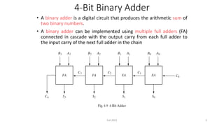
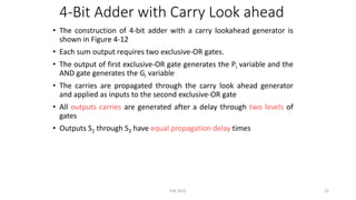
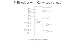
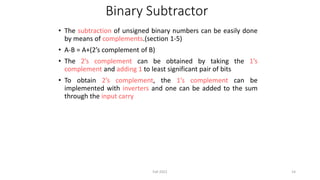
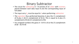
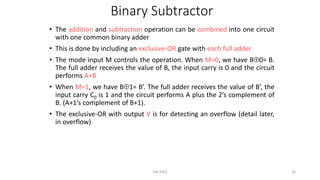
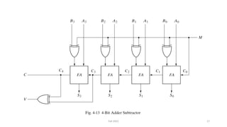
Chapter4: Combinational Logic
Lecture4- Design 4-bit Lookahead Carry Binary Adder-Subtractor
Circuit
Engr. Arshad Nazir, Asst Prof
Dept of Electrical Engineering
SEECS 1
Fall 2022
Objectives
• Study significant delay problems in Ripple Carry Binary Adder
• Design 4-Bit Lookahead Carry Binary Adder using Full-
Adders
• Learn overflow in Arithmetic Circuits
Fall 2022 2
4-Bit Binary Adder
• A binary adder is a digital circuit that produces the arithmetic sum of
two binary numbers.
• A binary adder can be implemented using multiple full adders (FA)
connected in cascade with the output carry from each full adder to
the input carry of the next full adder in the chain
3
Fall 2022
Carry Propagation
• The addition of two binary numbers in parallel implies that all the bits
of the augend and addend are available for computation at the same
time
• In any combinational circuit, the signal must propagate through the
gates before the correct output is available in the output terminals.
• The Total propagation time = propagation delay of a typical gate X the
number of gate levels
• The longest propagation delay time in a binary adder is the time it
takes the carry to propagate through the full adders.
• This is because each bit of the sum output depends on the value of
the input carry. This makes the binary adder very slow.
Fall 2022 4
Carry Propagation
• Since each bit of the sum output depends on the value of input carry,
the value of Si in any given stage in the adder will be in its steady state
final value only after the input carry to the stage has been propagated
• Consider output S3 in Figure 4-9. Inputs A3 and B3 are available as soon
as input signals are applied to the adder, however input carry C3
doesn’t settle to its final value until C2 is available from the previous
stage
• Similarly C2 has to wait for C1 and so on down to C0
• In this way only after the carry propagates and ripples through all
stages will the last output S3 and carry C4 settle to their final correct
value
Fall 2022 5
Carry Propagation
• The number of gate levels for the carry propagation can be found
from the circuit of the full adder
• The input and output variables use the subscript i to denote a typical
stage in the adder
• The signals at Pi and Gi settle to their steady state values after they
propagate through their respective gates
6
Fall 2022
Carry Propagation
• These two signals are common to all full adders and depend only on
the augend and addend bits
• The signal from the input carry Ci to the output carry Ci+1 propagates
through an AND gate and an OR gate, which constitutes two gate
levels
• If there are four full adders in the adder, the output carry C4 would
have 2 x 4 = 8 gate levels from C0 to C4.
• For an n-bit adder, there are 2n gate levels for the carry to propagate
from input to output
• The outputs of a combinational circuit will not be correct unless the
signals are given enough time to propagate through the gates
connected from inputs to outputs
• All other arithmetic operations are implemented by successive
additions, the time consumed during the addition process is very
critical.
7
Fall 2022
Carry Propagation
• One choice to reduce the carry propagation delay is to employ faster
gates but the most widely used technique for reducing the carry
propagation time in parallel adder is principle of carry lookahead
• Consider the circuit of full adder shown in fig 4-10
• If we define two binary variables
carry propagate: Pi = AiBi (Term associated with the propagation
of carry from Ci to Ci+1)
carry generate: Gi = AiBi (Produces 1 when both Ai and Bi are 1)
• Output sum and carry can be expressed as
sum: Si = PiCi
Carry: Ci+1 = Gi+PiCi
8
Fall 2022
Carry Propagation
• We now write the Boolean functions for the carry outputs of each
stage and substitute for each Ci, its value from the previous equation
Co= input carry
C1 = G0+P0C0
C2 = G1+P1C1
= G1+P1(G0+P0C0)
= G1+P1G0+P1P0C0
C3 = G2+P2C2
= G2+P2G1+P2P1G0+ P2P1P0C0
C4 = G3+P3C3
=G3+P3G2+P3P2G1+P3P2P1G0+P3P2P1P0C0
• Since the Boolean function for each output carry is expressed in sum of
products, each function can be implemented with one level of AND
gates followed by an OR gate (or by two-level NAND)
9
Fall 2022
Carry Look ahead Generator
• The four Boolean functions for C1, C2, C3 ,and C4 are implemented in
the carry look ahead generator shown in Figure 4-11
• Here C4 doesn’t have to wait for C3, C2 and C1 to propagate and C4 is
propagated at the same time as C1, C2, and C3.
10
Fall 2022
Carry Look ahead Generator
Fig 4-11 Logic Diagram of Carry Look ahead Generator
11
Fall 2022
4-Bit Adder with Carry Look ahead
• The construction of 4-bit adder with a carry lookahead generator is
shown in Figure 4-12
• Each sum output requires two exclusive-OR gates.
• The output of first exclusive-OR gate generates the Pi variable and the
AND gate generates the Gi variable
• The carries are propagated through the carry look ahead generator
and applied as inputs to the second exclusive-OR gate
• All outputs carries are generated after a delay through two levels of
gates
• Outputs S1 through S3 have equal propagation delay times
12
Fall 2022
4-Bit Adder with Carry Look ahead
13
Fall 2022
Binary Subtractor
• The subtraction of unsigned binary numbers can be easily done
by means of complements.(section 1-5)
• A-B = A+(2’s complement of B)
• The 2’s complement can be obtained by taking the 1’s
complement and adding 1 to least significant pair of bits
• To obtain 2’s complement, the 1’s complement can be
implemented with inverters and one can be added to the sum
through the input carry
14
Fall 2022
Binary Subtractor
• The circuit for subtracting A – B consists of an adder with inverters
placed between each data input B and the corresponding input of
full adder
• The input carry C0 must be equal to 1 when performing subtraction
• The operation thus performed becomes A plus the 1’s complement
of B plus 1 (A+1’s complement of B+1). This is equal to A plus 2’s
complement of B (A+2’s complement of B)
• For unsigned numbers this gives A – B if A ≥ B or the 2’s complement
of (B – A) if A<B
15
Fall 2022
Binary Subtractor
• The addition and subtraction operation can be combined into one circuit
with one common binary adder
• This is done by including an exclusive-OR gate with each full adder
• The mode input M controls the operation. When M=0, we have B0= B.
The full adder receives the value of B, the input carry is 0 and the circuit
performs A+B
• When M=1, we have B1= B’. The full adder receives the value of B’, the
input carry C0 is 1 and the circuit performs A plus the 2’s complement of
B. (A+1’s complement of B+1).
• The exclusive-OR with output V is for detecting an overflow (detail later,
in overflow)
16
Fall 2022
17
Fall 2022
Overflow
• When two numbers of n digits are added and sum occupies n+1 digits
we say that an overflow occurred
• Overflow is problem in digital computers because the number of bits
that hold the number (limited storage) is finite and a result that
contains n+1 can’t be accommodated.
• The detection of an overflow after the addition of two binary
numbers depends on whether the numbers are considered to be
signed or unsigned
• When two unsigned numbers are added an overflow is detected from
the end carry out of the most significant position
• In the case of signed numbers, the leftmost bit always represent the
sign and negative numbers are in 2’s complement form
Fall 2022 18
Overflow
• When two signed numbers are added, the sign bit is treated as part of
the number and end carry doesn’t indicate an overflow
• An overflow can’t occur after an addition if one number is positive
and the other is negative, since adding a positive number to a
negative number produces a result which is smaller than the larger of
the two original numbers.
• An overflow may occur if the two numbers added are both positive or
both negative
• For n-bit registers, the range of numbers (signed numbers) that each
register can accommodate is from binary 2n-1-1 to binary –2n-1.
Fall 2022 19
Overflow
• For 8-bit registers, the range of numbers that each register can
accommodate is from binary +127 to binary –128
• Consider two signed numbers +70 and +80 stored in two 8-bit registers.
The sum of two numbers is +150 which exceeds the capacity of eight bit
register
Note: Negative numbers are in 2’s complement form
Fall 2022 20
Overflow
• If we just consider the 8-bit result from the last example, we go wrong
as we
Add two positive numbers and obtain a negative number
Add two negative numbers and obtain a positive number
• The carry out of sign bit position is taken as the sign bit of the result,
then the 9-bit answer so obtained will be correct. This answer can’t be
accommodated within 8-bits we say that an overflow has occurred
• An overflow has occurred if carry into the sign bit position and carry
out of the sign bit position are not equal. This can be found by
applying the two carries to an exclusive-OR gate. 1 at the output of
the gate indicates overflow
V=0, no overflow; V=1, overflow
Fall 2022 21
The End
22
Fall 2022

Lecture4 Chapter4- Design 4-bit Lookahead Carry Binary Adder-Subtractor Circuit.pdf

  • 1.
    Chapter4: Combinational Logic Lecture4-Design 4-bit Lookahead Carry Binary Adder-Subtractor Circuit Engr. Arshad Nazir, Asst Prof Dept of Electrical Engineering SEECS 1 Fall 2022
  • 2.
    Objectives • Study significantdelay problems in Ripple Carry Binary Adder • Design 4-Bit Lookahead Carry Binary Adder using Full- Adders • Learn overflow in Arithmetic Circuits Fall 2022 2
  • 3.
    4-Bit Binary Adder •A binary adder is a digital circuit that produces the arithmetic sum of two binary numbers. • A binary adder can be implemented using multiple full adders (FA) connected in cascade with the output carry from each full adder to the input carry of the next full adder in the chain 3 Fall 2022
  • 4.
    Carry Propagation • Theaddition of two binary numbers in parallel implies that all the bits of the augend and addend are available for computation at the same time • In any combinational circuit, the signal must propagate through the gates before the correct output is available in the output terminals. • The Total propagation time = propagation delay of a typical gate X the number of gate levels • The longest propagation delay time in a binary adder is the time it takes the carry to propagate through the full adders. • This is because each bit of the sum output depends on the value of the input carry. This makes the binary adder very slow. Fall 2022 4
  • 5.
    Carry Propagation • Sinceeach bit of the sum output depends on the value of input carry, the value of Si in any given stage in the adder will be in its steady state final value only after the input carry to the stage has been propagated • Consider output S3 in Figure 4-9. Inputs A3 and B3 are available as soon as input signals are applied to the adder, however input carry C3 doesn’t settle to its final value until C2 is available from the previous stage • Similarly C2 has to wait for C1 and so on down to C0 • In this way only after the carry propagates and ripples through all stages will the last output S3 and carry C4 settle to their final correct value Fall 2022 5
  • 6.
    Carry Propagation • Thenumber of gate levels for the carry propagation can be found from the circuit of the full adder • The input and output variables use the subscript i to denote a typical stage in the adder • The signals at Pi and Gi settle to their steady state values after they propagate through their respective gates 6 Fall 2022
  • 7.
    Carry Propagation • Thesetwo signals are common to all full adders and depend only on the augend and addend bits • The signal from the input carry Ci to the output carry Ci+1 propagates through an AND gate and an OR gate, which constitutes two gate levels • If there are four full adders in the adder, the output carry C4 would have 2 x 4 = 8 gate levels from C0 to C4. • For an n-bit adder, there are 2n gate levels for the carry to propagate from input to output • The outputs of a combinational circuit will not be correct unless the signals are given enough time to propagate through the gates connected from inputs to outputs • All other arithmetic operations are implemented by successive additions, the time consumed during the addition process is very critical. 7 Fall 2022
  • 8.
    Carry Propagation • Onechoice to reduce the carry propagation delay is to employ faster gates but the most widely used technique for reducing the carry propagation time in parallel adder is principle of carry lookahead • Consider the circuit of full adder shown in fig 4-10 • If we define two binary variables carry propagate: Pi = AiBi (Term associated with the propagation of carry from Ci to Ci+1) carry generate: Gi = AiBi (Produces 1 when both Ai and Bi are 1) • Output sum and carry can be expressed as sum: Si = PiCi Carry: Ci+1 = Gi+PiCi 8 Fall 2022
  • 9.
    Carry Propagation • Wenow write the Boolean functions for the carry outputs of each stage and substitute for each Ci, its value from the previous equation Co= input carry C1 = G0+P0C0 C2 = G1+P1C1 = G1+P1(G0+P0C0) = G1+P1G0+P1P0C0 C3 = G2+P2C2 = G2+P2G1+P2P1G0+ P2P1P0C0 C4 = G3+P3C3 =G3+P3G2+P3P2G1+P3P2P1G0+P3P2P1P0C0 • Since the Boolean function for each output carry is expressed in sum of products, each function can be implemented with one level of AND gates followed by an OR gate (or by two-level NAND) 9 Fall 2022
  • 10.
    Carry Look aheadGenerator • The four Boolean functions for C1, C2, C3 ,and C4 are implemented in the carry look ahead generator shown in Figure 4-11 • Here C4 doesn’t have to wait for C3, C2 and C1 to propagate and C4 is propagated at the same time as C1, C2, and C3. 10 Fall 2022
  • 11.
    Carry Look aheadGenerator Fig 4-11 Logic Diagram of Carry Look ahead Generator 11 Fall 2022
  • 12.
    4-Bit Adder withCarry Look ahead • The construction of 4-bit adder with a carry lookahead generator is shown in Figure 4-12 • Each sum output requires two exclusive-OR gates. • The output of first exclusive-OR gate generates the Pi variable and the AND gate generates the Gi variable • The carries are propagated through the carry look ahead generator and applied as inputs to the second exclusive-OR gate • All outputs carries are generated after a delay through two levels of gates • Outputs S1 through S3 have equal propagation delay times 12 Fall 2022
  • 13.
    4-Bit Adder withCarry Look ahead 13 Fall 2022
  • 14.
    Binary Subtractor • Thesubtraction of unsigned binary numbers can be easily done by means of complements.(section 1-5) • A-B = A+(2’s complement of B) • The 2’s complement can be obtained by taking the 1’s complement and adding 1 to least significant pair of bits • To obtain 2’s complement, the 1’s complement can be implemented with inverters and one can be added to the sum through the input carry 14 Fall 2022
  • 15.
    Binary Subtractor • Thecircuit for subtracting A – B consists of an adder with inverters placed between each data input B and the corresponding input of full adder • The input carry C0 must be equal to 1 when performing subtraction • The operation thus performed becomes A plus the 1’s complement of B plus 1 (A+1’s complement of B+1). This is equal to A plus 2’s complement of B (A+2’s complement of B) • For unsigned numbers this gives A – B if A ≥ B or the 2’s complement of (B – A) if A<B 15 Fall 2022
  • 16.
    Binary Subtractor • Theaddition and subtraction operation can be combined into one circuit with one common binary adder • This is done by including an exclusive-OR gate with each full adder • The mode input M controls the operation. When M=0, we have B0= B. The full adder receives the value of B, the input carry is 0 and the circuit performs A+B • When M=1, we have B1= B’. The full adder receives the value of B’, the input carry C0 is 1 and the circuit performs A plus the 2’s complement of B. (A+1’s complement of B+1). • The exclusive-OR with output V is for detecting an overflow (detail later, in overflow) 16 Fall 2022
  • 17.
  • 18.
    Overflow • When twonumbers of n digits are added and sum occupies n+1 digits we say that an overflow occurred • Overflow is problem in digital computers because the number of bits that hold the number (limited storage) is finite and a result that contains n+1 can’t be accommodated. • The detection of an overflow after the addition of two binary numbers depends on whether the numbers are considered to be signed or unsigned • When two unsigned numbers are added an overflow is detected from the end carry out of the most significant position • In the case of signed numbers, the leftmost bit always represent the sign and negative numbers are in 2’s complement form Fall 2022 18
  • 19.
    Overflow • When twosigned numbers are added, the sign bit is treated as part of the number and end carry doesn’t indicate an overflow • An overflow can’t occur after an addition if one number is positive and the other is negative, since adding a positive number to a negative number produces a result which is smaller than the larger of the two original numbers. • An overflow may occur if the two numbers added are both positive or both negative • For n-bit registers, the range of numbers (signed numbers) that each register can accommodate is from binary 2n-1-1 to binary –2n-1. Fall 2022 19
  • 20.
    Overflow • For 8-bitregisters, the range of numbers that each register can accommodate is from binary +127 to binary –128 • Consider two signed numbers +70 and +80 stored in two 8-bit registers. The sum of two numbers is +150 which exceeds the capacity of eight bit register Note: Negative numbers are in 2’s complement form Fall 2022 20
  • 21.
    Overflow • If wejust consider the 8-bit result from the last example, we go wrong as we Add two positive numbers and obtain a negative number Add two negative numbers and obtain a positive number • The carry out of sign bit position is taken as the sign bit of the result, then the 9-bit answer so obtained will be correct. This answer can’t be accommodated within 8-bits we say that an overflow has occurred • An overflow has occurred if carry into the sign bit position and carry out of the sign bit position are not equal. This can be found by applying the two carries to an exclusive-OR gate. 1 at the output of the gate indicates overflow V=0, no overflow; V=1, overflow Fall 2022 21
  • 22.