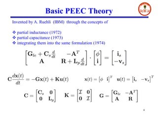
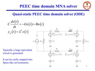
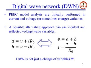
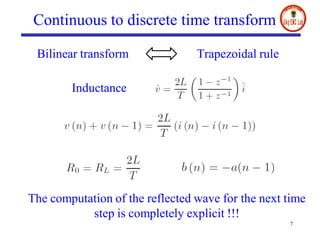
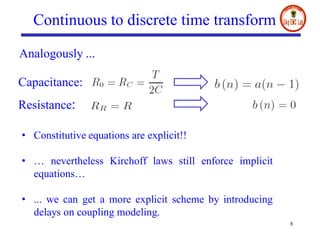
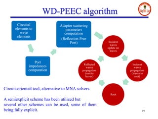
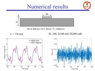
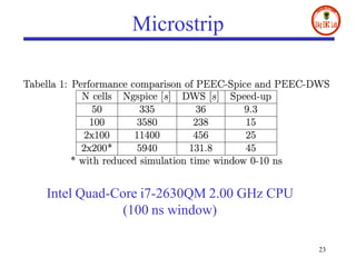
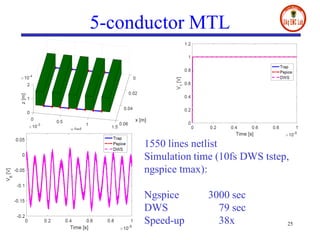
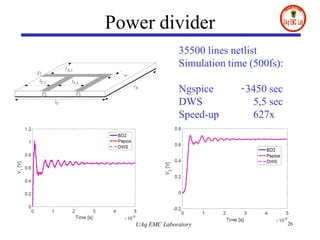
- The document presents a digital wave formulation of the partial element equivalent circuit (PEEC) method for quasi-static electromagnetic problems.
- It converts traditional PEEC networks into an equivalent digital wave network using scattering parameters and reflection-free ports. This allows for a more explicit solution scheme compared to matrix node analysis approaches.
- Numerical results on microstrip and multilayer structures show significant speed-ups of up to 627 times compared to traditional SPICE solvers when using the proposed digital wave PEEC approach.
Topography and sediments of the floor of the Bay of Bengal
DIGITAL WAVE FORMULATION OF PEEC METHOD (SLIDES)
1. Digital Wave Formulation of Quasi-Static
Partial Element Equivalent Circuit Method
Piero Belforte, Luigi Lombardi,
Daniele Romano, Giulio Antonini
piero.belforte@gmail.com , luigilombardi89@gmail.com,
daniele.romano.vis@gmail.com, giulio.antonini@univaq.it,
SPI 2016
Torino, May 10, 2016
2. Summary
o Basic PEEC theory
o Digital Wave Networks
o Digital Wave PEEC Network
o Solution algorithm
o Digital Wave Simulator
o Numerical results
o Conclusions
2
4. Basic PEEC Theory
Invented by A. Ruehli (IBM) through the concepts of
partial inductance (1972)
partial capacitance (1973)
integrating them into the same formulation (1974)
4
5. PEEC time domain MNA solver
Quasi-static PEEC time domain solver (ODE)
T
p
dx t
C Gx t Bu t
dt
y t L x t
5
Typically a large equivalent
circuit is generated.
It can be easily mapped into
Spice-like environments.
6. Digital wave network (DWN)
6
• PEEC model analysis are tipically performed in
current and voltage (or sometimes charge) variables.
• A possible alternative approach can use incident and
reflected voltage wave variables.
DWN is not just a change of variables !!!
7. 7
Continuous to discrete time transform
Bilinear transform Trapezoidal rule
Inductance
The computation of the reflected wave for the next time
step is completely explicit !!!
8. 8
Continuous to discrete time transform
Capacitance:
Resistance:
Analogously ...
• Constitutive equations are explicit!!
• … nevertheless Kirchoff laws still enforce implicit
equations…
• ... we can get a more explicit scheme by introducing
delays on coupling modeling.
9. Adaptors
UAq EMC Laboratory 9
In order to transfer signal (voltages or currents) between circuital
elements we use series or parallel connection.
In the wave domain the equivalent concept is represented by adaptors.
12. Marx model for inductive coupling
12
Multiple coupling requires the
computation of reluctances
(acceleration techniques).
Mutual inductors are
delayed by one time step.
13. Link model for inductive coupling
13
Equivalent digital network for the inductive
coupling Pi model
Link model for the inductive coupling Pi
model
16. Equivalent digital network
16
ASc adaptors connect the capacitive
portion of the PEEC model
ASs and ASL connect source and load
respectively
NL parallel adaptors allow us to represent
the Marx model
ASRL adaptors build the RL branches
equivalent
17. 17
Root of the digital network
The N parallel adaptors
will become the nodes of the Root
The AS series adaptors
will become the branches of the Root
We have a loop that prevents
the explicit resolution of the
innermost part of the digital
network.
20. Digital Wave Simulator (DWS)
• Development started at CSELT Labs (Turin) in 1974 by P. Belforte & G.
Guaschino for design of high-speed digital systems
• From 1986 to 2001 at HDT (Turin) as general purpose Spice-like simulator
(SPRINT). SI/PI/EMC applications included PRESTO (post-layout),
EMIR (emissions) and THRIS in cooperation with CSELT (Qualification
tool)
• In 1998 at HDT first DWS-PEEC application (3D_PEEC)
• From 2001 to present as DWS including Multi-gigabit applications as
HiSAFE for Cisco Systems (P. Belforte)
• From 2012 also as Spicy SWAN cloud-based app
• From Feb. 2016 new PEEC-DWS developments in a cooperation driven by
P.Belforte and G.Antonini.
20
21. DWS early applications (1975)
UAq EMC Laboratory 21
CSELT LABS: ETA (Easy Transient Analysis) application to the design of a .5Gbps
high-speed Multichip Module. A TDR-based wideband measurement system was
included in the Digital Wave modeling & simulation environment.
22. DWS main features
• Conversion of a Spice-like netlist into a Digital Network
equivalent including circuital elements and nodes as
scattering blocks exchanging waves at their ports.
• DSP oriented solution apart from the root. DFLs solved by
port-matching calculation scheduling
• Wideband SI/PI/EMC applications
• Complementary to Spice
Detailed documents available at
https://www.researchgate.net/profile/Piero_Belforte
22
27. Conclusions
27
• A Digital Wave (DW) model of quasi-static PEEC circuits has
been proposed.
• A proper scheduling of calculations has been used.
• Significant speed-ups (up to 627x) have been experienced
replacing MNA Spice-like solvers with DWS.
• DWS speed-up increases with PEEC model complexity.
• A semi-explicit scheme has been tested so far but...
• ...at least 7 more implementations including fully explicit schemes
with different stability properties and performances are possible.
They are under investigation.
28. Future work
UAq EMC Laboratory 28
• Inclusion of physical delays leading also to a fully
explicit scheme.
• Stability and passivity analysis of delayed wave digital
network.
• Developement of a in-house Digital Wave PEEC Solver
exploiting the features of all the possible topologies.
• Inclusion of skin-effect and dielectric losses.