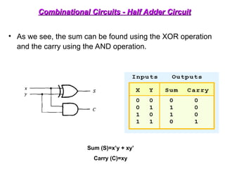
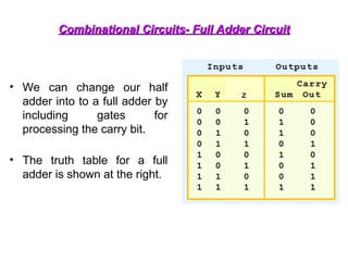
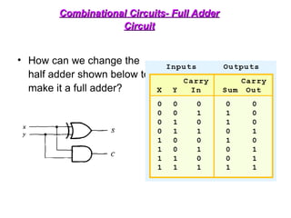
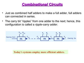
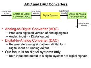
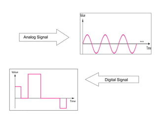
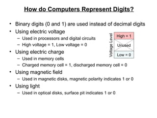
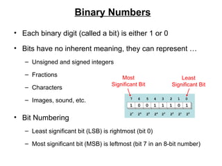
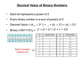
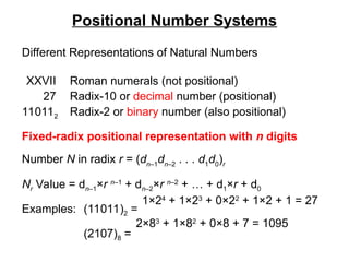
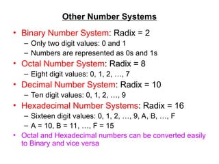
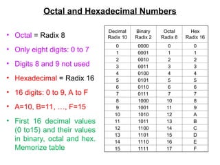
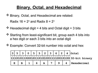
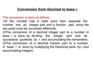
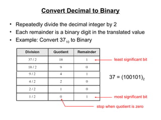
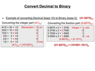
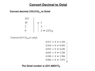
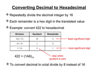
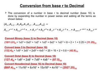
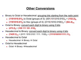
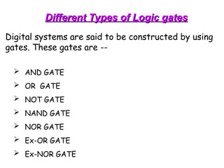
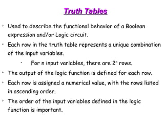
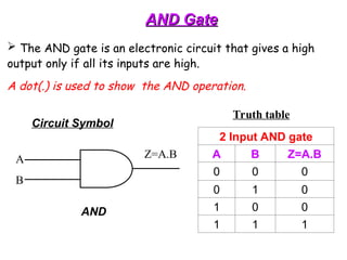
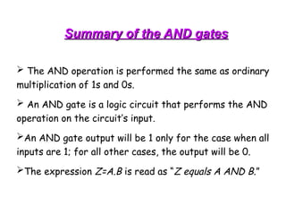
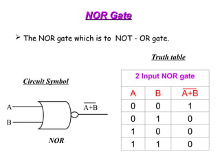
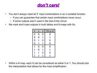
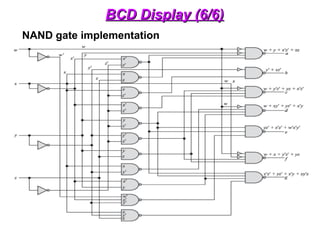
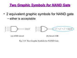
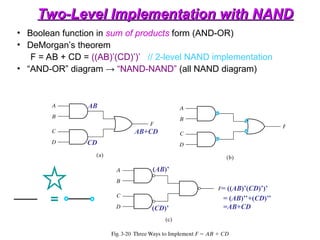
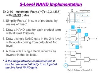
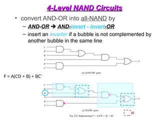
The document provides an overview of number systems and digital logic design, covering topics such as binary, octal, decimal, and hexadecimal systems, along with various data conversion techniques. It explores the structure of digital systems, key components like analog-to-digital converters, and basic logic gates including AND, OR, NAND, and NOR gates. Additionally, it delves into Boolean algebra and its application in analyzing and designing logic circuits.


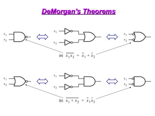


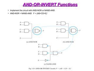
![OR-AND-INVERT Functions
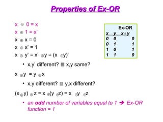
OR-AND-INVERT Functions
• Implement the circuit with OR-NAND or NOR-OR
• OR-NAND = NOR-OR F = [(A+B)(C+D)E)]’](https://image.slidesharecdn.com/dldlecturenotes-240922053217-6e05a007/85/Digital-Logic-Design-Lecture-Notes-1-ppt-105-320.jpg)
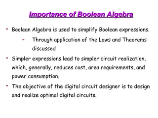
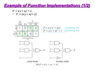
![Example of Function Implementations (2/2)
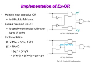
Example of Function Implementations (2/2)
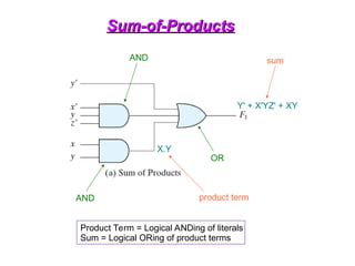
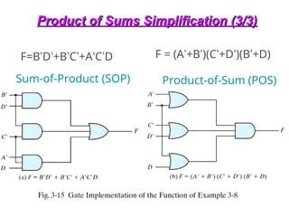
F = x’y’z’ + xyz’
F’=(x+y+z)(x’+y’+z) F = [(x+y+z)(x’+y’+z)]’
(combining 1’s)
(combining 0’s)](https://image.slidesharecdn.com/dldlecturenotes-240922053217-6e05a007/85/Digital-Logic-Design-Lecture-Notes-1-ppt-106-320.jpg)
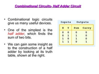
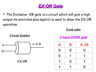
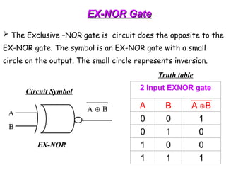
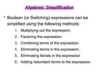
![Exclusive-OR (Ex-OR)
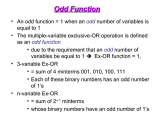
Exclusive-OR (Ex-OR)
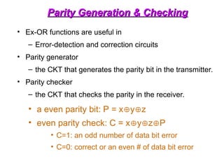
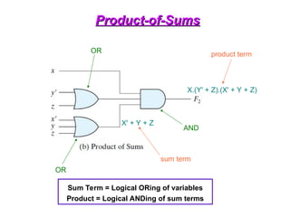
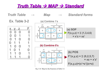
• Exclusive-OR (Ex-OR)
x y = xy’ + x’y
• x=1 or y=1 but not both
• different inputs output = 1
• only one input equal to 1 output = 1
• Exclusive-NOR
(x ʘ y) = xy + x’y’
• same inputs (both=1 or both=0) output = 1
⇒
• Ex-OR is the complement of Exclusive-NOR
[proof] (x y)’ = (xy’+x’y)’ = (x’+y)(x+y’)
= xy +x’y’
Ex-OR
x y x♁y
0 0
0
0 1
1
1 0
1
1 1
0
Ex-NOR
x y (x♁y)’
0 0
1
0 1
0
1 0
0
1 1
1](https://image.slidesharecdn.com/dldlecturenotes-240922053217-6e05a007/85/Digital-Logic-Design-Lecture-Notes-1-ppt-109-320.jpg)