Download to read offline
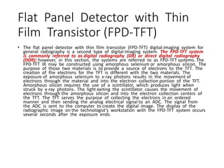


Digital imaging systems like photostimulable storage phosphor (PSP) plates, flat panel detectors with thin film transistors (FPD-TFT), and charged couple devices (CCD) have created misconceptions due to their various acronyms and designs. PSP plates capture and store x-ray exposure electrons, which are released as light during reading and converted to digital images. FPD-TFT systems directly capture electrons using amorphous selenium or silicon and thin film transistors. CCD systems use scintillators to convert x-rays to light, which is focused onto CCDs and converted to electrons and digital images. Regardless of appearance or how images are captured, all digital systems have a


